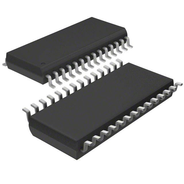
CY24272
Rambus XDR™ Clock Generator with Zero SDA Hold Time
Rambus‚ XDR™ Clock Generator with Zero SDA Hold Time
Features
■ ■
Meets Rambus Extended Data Rate (XDR™) clocking requirements 25 ps typical cycle-to-cycle jitter ❐ –135 dBc/Hz typical phase noise at 20 MHz offset 100 or 133 MHz differential clock input 300–667 MHz high speed clock support Quad (open drain) differential output drivers Supports frequency multipliers: 3, 4, 5, 6, 9/2 and 15/4 Spread Aware™ 2.5 V operation 28-pin TSSOP package
Table 1. Device Comparison CY24271 SDA hold time = 300 ns (SMBus compliant) RRC = 200 typical (Rambus standard drive) CY24272 SDA hold time = 0 ns (I2C compliant) RRC = 295 minimum (Reduced output drive)
■ ■ ■ ■ ■ ■ ■
Logic Block Diagram
/BYPASS EN
EN RegA
CLK0 CLK0B EN RegB CLK1 CLK1B EN RegC REFCLK,REFCLKB
Bypass MUX
PLL
CLK2 CLK2B
EN RegD CLK3 CLK3B
SCL
SDA
ID0
ID1
Cypress Semiconductor Corporation Document Number: 001-42414 Rev. *A
•
198 Champion Court
•
San Jose, CA 95134-1709 • 408-943-2600 Revised February 17, 2011
[+] Feedback
�CY24272
Contents
Pinouts .............................................................................. 3 PLL Multiplier .................................................................... 4 Input Clock Signal ............................................................ 4 Modes of Operation .......................................................... 4 Device ID and SMBus Device Address ........................... 5 SMBus Protocol ................................................................ 5 SMBus Data Byte Definitions .......................................... 5 Absolute Maximum Conditions ....................................... 7 DC Operating Conditions ................................................. 8 DC Electrical Specifications ............................................ 9 AC Operating Conditions ................................................. 9 AC Electrical Specification ............................................ 10 Test and Measurement Setup ........................................ 11 Example External Resistor Values and Termination Voltages for a 50 W Channel ............ 11 Signal Waveforms .......................................................... 11 Jitter ................................................................................. 11 Ordering Information ...................................................... 13 Ordering Code Definitions ......................................... 13 Package Drawing and Dimension ................................. 13 Acronyms ........................................................................ 14 Document Conventions ................................................. 14 Units of Measure ....................................................... 14 Document History Page ................................................. 15 Sales, Solutions, and Legal Information ...................... 16 Worldwide Sales and Design Support ....................... 16 Products .................................................................... 16 PSoC Solutions ......................................................... 16
Document Number: 001-42414 Rev. *A
Page 2 of 16
[+] Feedback
�CY24272
Pinouts
Figure 1. Pin Diagram - 28-pin TSSOP
VDDP VSSP ISET VSS REFCLK REFCLKB VDDC VSSC SCL SDA EN ID0 ID1 /BYPASS
1 2 3 4 5 6 7 8 9 10 11 12 13 14
28 27 26 25 24 23 22 21 20 19 18 17 16 15
VDD CLK0 CLK0B VSS CLK1 CLK1B VDD VSS CLK2 CLK2B VSS CLK3 CLK3B VDD
CY24272
Table 2. Pin Definition - 28-pin TSSOP Pin No. 1 2 3 4 5 6 7 8 9 10 11 12 13 14 15 16 17 18 19 20 21 22 23 24 25 26 27 28 Name VDDP VSSP ISET VSS REFCLK REFCLKB VDDC VSSC SCL SDA EN ID0 ID1 /BYPASS VDD CLK3B CLK3 VSS CLK2B CLK2 VSS VDD CLK1B CLK1 VSS CLK0B CLK0 VDD IO PWR GND I GND I I PWR GND I I I I I I PWR O O GND O O GND PWR O O GND O O PWR Ground Set clock driver current (external resistor) Ground Reference clock input (connect to clock source) Complement of reference clock (connect to clock source) 2.5 V power supply for core Ground SMBus clock (connect to SMBus) SMBus data (connect to SMBus) Output Enable (CMOS signal) Device ID (CMOS signal) Device ID (CMOS signal) REFCLK bypassing PLL (CMOS signal) Power supply for outputs Complement clock output Clock output Ground Complement clock output Clock output Ground Power supply for outputs Complement clock output Clock output Ground Complement clock output Clock output Power supply for outputs Description 2.5 V power supply for phased lock loop (PLL)
Document Number: 001-42414 Rev. *A
Page 3 of 16
[+] Feedback
�CY24272
PLL Multiplier
Table 3 shows the frequency multipliers in the PLL, selectable by programming the SMBus registers MULT0, MULT1, and MULT2. Default multiplier at power up is 4. Table 3. PLL Multiplier Selection Register MULT2 0 0 0 0 1 1 1 1 MULT1 0 0 1 1 0 0 1 1 MULT0 0 1 0 1 0 1 0 1 Frequency Multiplier 3 4 5 6 Reserved 9/2 Reserved 15/4 Output Frequency (MHz) REFCLK = 100 MHz[1], REFSEL = 0 REFCLK = 133 MHz[1], REFSEL = 1 300 400[2] 500 600 – 450 – 375 400 – 667 – – 600 – 500
Input Clock Signal
The XCG receives either a differential (REFCLK/REFCLKB) or a single-ended reference clocking input (REFCLK). When the reference input clock is from a different clock source, it must meet the voltage levels and timing requirements listed in DC Operating Conditions on page 8 and AC Operating Conditions on page 9. For a single-ended clock input, an external voltage divider and a supply voltage, as shown in Figure 2 on page 7, provide a reference voltage VTH at the REFCLKB pin. This determines the proper trip point of REFCLK. For the range of VTH specified in DC Operating Conditions on page 8, the outputs also meet the DC and AC Operating Conditions tables. Table 4. SMBus Device Addresses for CY24272 XCG Device 0 1 2 3 Operation Write Read Write Read Write Read Write Read Hex Address D8 D9 DA DB DC DD DE DF 1 1 0
Modes of Operation
The modes of operation are determined by the logic signals applied to the EN and /BYPASS pins and the values in the five SMBus Registers: RegTest, RegA, RegB, RegC, and RegD. Table 5 on page 5 shows selection from one to all four of the outputs, the Outputs Disabled Mode (EN = low), and Bypass Mode (EN = high, /BYPASS = low). There is an option reserved for vendor test. Disabled outputs are set to High Z. At power up, the SMBus registers default to the last entry in Table 6 on page 6. The value at RegTest is 0. The values at RegA, RegB, RegC, and RegD are all ‘1’. Thus, all outputs are controlled by the logic applied to EN and /BYPASS.
8-bit SMBus Device Address Including Operation Five Most Significant Bits ID1 0 0 1 1 1 1 0 1 ID0 0 1 WR# / RD 0 1 0 1 0 1 0 1
Notes 1. Output frequencies shown in Table 3 are based on nominal input frequencies of 100 MHz and 133.3 MHz. The PLL multipliers are applicable to spread spectrum modulated input clock with maximum and minimum input cycle time. The REFSEL bit in SMBus 81h is set correctly as shown. 2. Default PLL multiplier at power up.
Document Number: 001-42414 Rev. *A
Page 4 of 16
[+] Feedback
�CY24272
Table 5. Modes of Operation for CY24272 EN L H H H H H H H H H H H H H H H H H H /BYPASS RegTest RegA RegB RegC RegD CLK0/CLK0B X X L H H H H H H H H H H H H H H H H X 1 0 0 0 0 0 0 0 0 0 0 0 0 0 0 0 0 0[4] X X X 0 0 0 0 0 0 0 0 1 1 1 1 1 1 1 1[4] X X X 0 0 0 0 1 1 1 1 0 0 0 0 1 1 1 1[4] X X X 0 0 1 1 0 0 1 1 0 0 1 1 0 0 1 1[4] X X X 0 1 0 1 0 1 0 1 0 1 0 1 0 1 0 1[4] REFCLK/ REFCLKB[3] High Z High Z High Z High Z High Z High Z High Z High Z CLK/CLKB CLK/CLKB CLK/CLKB CLK/CLKB CLK/CLKB CLK/CLKB CLK/CLKB CLK/CLKB High Z CLK1/CLK1B High Z REFCLK/ REFCLKB High Z High Z High Z High Z CLK/CLKB CLK/CLKB CLK/CLKB CLK/CLKB High Z High Z High Z High Z CLK/CLKB CLK/CLKB CLK/CLKB CLK/CLKB CLK2/CLK2B CLK3/CLK3B High Z REFCLK/ REFCLKB High Z High Z CLK/CLKB CLK/CLKB High Z High Z CLK/CLKB CLK/CLKB High Z High Z CLK/CLKB CLK/CLKB High Z High Z CLK/CLKB CLK/CLKB High Z REFCLK/ REFCLKB High Z CLK/CLKB High Z CLK/CLKB High Z CLK/CLKB High Z CLK/CLKB High Z CLK/CLKB High Z CLK/CLKB High Z CLK/CLKB High Z CLK/CLKB
Reserved for Vendor Test
Device ID and SMBus Device Address
The device ID (ID0 and ID1) is a part of the SMBus device 8-bit address. The least significant bit of the address designates a write or read operation. Table 4 on page 4 shows the addresses for four CY24272 devices on the same SMBus.
SMBus Data Byte Definitions
Three data bytes are defined for the CY24272. Byte 0 is for programming the PLL multiplier registers and clock output registers. The definition of Byte 2 is shown in Table 6 on page 6, Table 7 on page 6, and Table 8 on page 6. The upper five bits are the revision numbers of the device and the lower three bits are the ID numbers assigned to the vendor by Rambus.
SMBus Protocol
The CY24272 is a slave receiver supporting operations in the word and byte modes described in sections 5.5.4 and 5.5.5 of the SMBus Specification 2.0. DC specifications are modified to Rambus standard to support 1.8, 2.5, and 3.3 volt devices. Time out detection and packet error protocol SMBus features are not supported. Hold time for SDA is reduced relative to the CY24271, so that it is compatible with I2C.
Notes 3. Bypass Mode: REFCLK bypasses the PLL to the output drivers. 4. Default mode of operation is at power up.
Document Number: 001-42414 Rev. *A
Page 5 of 16
[+] Feedback
�CY24272
Table 6. Command Code 80h[5] Bit 7 6 5 4 3 2 1 0 Register Reserved MULT2 MULT1 MULT0 RegA RegB RegC RegD POD 0 0 0 1 1 1 1 1 Type RW RW RW RW RW RW RW RW Clock 0 Output Select Clock 1 Output Select Clock 2 Output Select Clock 3 Output Select Reserved (no internal function) PLL Multiplier Select (reference Table 3 on page 4) Description
Table 7. Command Code 81h[5] Bit 7 6 5 4 3 2 1 0 Register Reserved Reserved Reserved Reserved Reserved REFSEL Reserved RegTest POD 0 0 0 0 1 0 0 0 Type RW RW RW RW RW RW RW RW Reserved (must be set to ‘1’ for proper operation) Reference Frequency Select (reference Table 3 on page 4) Reserved (must be set to ‘0’ for proper operation) Reserved (must be set to ‘0’ for proper operation) Reserved (no internal function) Description
Table 8. Command Code 82h[5] Bit 7 6 5 4 3 2 1 0 Vendor ID Register Device Revision Number POD ? ? ? ? ? 0 1 0 Type RO RO RO RO RO RO RO RO Rambus assigned Vendor ID Code Description Contact factory for Device Revision Number information.
Note 5. RW = Read and Write, RO = Read Only, POD = Power on default. See Table 3 on page 4 for PLL multipliers and Table 5 on page 5 for clock output selections.
Document Number: 001-42414 Rev. *A
Page 6 of 16
[+] Feedback
�CY24272
Figure 2. Differential and Single-Ended Clock Inputs
Supply Voltage
REFCLKB REFCLK
V TH Input REFCLK XDR Clock Generator XDR Clock Generator Input
Differential Input
Single-ended Input
Absolute Maximum Conditions
Parameter VDD VDDC VDDP VIN Description Clock Buffer Supply Voltage Core Supply Voltage PLL Supply Voltage Input Voltage (SCL and SDA) Input Voltage (REFCLK/REFCLKB) Input Voltage TS TA TJ ØJA ESDHBM Temperature, Storage Temperature, Operating Ambient Temperature, Junction Junction to Ambient thermal resistance Relative to VSS Relative to VSS Relative to VSS Non-functional Functional Functional Zero air flow Condition Min –0.5 –0.5 –0.5 –0.5 –0.5 –0.5 –65 0 – – 2000 Max 4.6 4.6 4.6 4.6 VDD + 1.0 VDD + 0.5 150 70 150 100 – Unit V V V V V V °C °C °C °C/W V
ESD Protection (Human Body Model) MIL-STD-883, Method 3015
Document Number: 001-42414 Rev. *A
Page 7 of 16
[+] Feedback
�CY24272
DC Operating Conditions
Parameter VDDP VDDC VDD VIHCLK VILCLK VIXCLK[6] VIXCLK[6] VIH VIL VIH,SM VIL,SM VTH[8] VIH,SE VIL,SE TA Supply Voltage for PLL Supply Voltage for Core Supply Voltage for Clock Buffers Input High Voltage, REFCLK/REFCLKB Input Low Voltage, REFCLK/REFCLKB Crossing Point Voltage, REFCLK/REFCLKB Difference in Crossing Point Voltage, REFCLK/REFCLKB Input Signal High Voltage at ID0, ID1, EN, and /BYPASS Input Signal Low Voltage at ID0, ID1, EN, and /BYPASS Input Signal High Voltage at SCL and SDA[7] Input Signal Low Voltage at SCL and SDA Input Threshold Voltage for single-ended REFCLK Input Signal High Voltage for single-ended REFCLK Input Signal Low Voltage for single-ended REFCLK Ambient Operating Temperature Description Condition 2.5 V ± 5% 2.5 V ± 5% 2.5 V ± 5% Min 2.375 2.375 2.375 0.6 –0.15 200 – 1.4 –0.15 1.4 –0.15 0.35 VTH + 0.3 –0.15 0 Max 2.625 2.625 2.625 0.95 +0.15 550 150 2.625 0.8 3.465 0.8 0.5 × VDD 2.625 VTH – 0.3 70 Unit V V V V V mV mV V V V V V V V °C
Notes 6. Not 100% tested except VIXCLK and VIXCLK. Parameters guaranteed by design and characterizations, not 100% tested in production. 7. This range of SCL and SDA input high voltage enables the CY24272 for use with 3.3 V, 2.5 V, or 1.8 V SMBus voltages. 8. Single-ended operation guaranteed only when 0.8 < (VIH,SE – VTH)/(VTH – VIL,SE) < 1.2.
Document Number: 001-42414 Rev. *A
Page 8 of 16
[+] Feedback
�CY24272
AC Operating Conditions
The AC operating conditions follow.[9] Parameter tCYCLE,IN Description REFCLK, REFCLKB input cycle time Condition REFSEL = 0, /BYPASS = High REFSEL = 1, /BYPASS = High /BYPASS = Low tJIT,IN(cc) tDCIN[11] tRIN / tFIN tRIN / tFIN pMIN[12] fMIN[12] tSR,IN CIN,REF CIN,CMOS fSCL Input Cycle to Cycle Jitter[10] Input Duty Cycle Rise and Fall Times Over 10,000 cycles Measured at 20%–80% of input voltage for REFCLK and REFCLKB inputs Min 9 7 4 – 40% 175 Max 11 8 – 185 60% 700 Unit ns ns ns ps tCYCLE ps
Rise and Fall Times Difference Modulation Index for triangular modulation Modulation Index for non-triangular modulation Input Frequency Modulation Input Slew Rate (measured at 20%–80% of input voltage) for REFCLK Capacitance at REFCLK inputs Capacitance at CMOS inputs SMBus clock frequency input in SCL pin
– – – 30 1 – – DC
150 0.6 0.5[13] 33 4 7 10 100
ps % % kHz V/ns pF pF kHz
DC Electrical Specifications
Parameter VOX[9] VCOS[9] VOL,ABS VISET IDD[17] IDD[17] IOL/IREF IOL,ABS VOL,SDA IOL,SDA IOZ ZOUT Description Differential output crossing point voltage[14] Output voltage swing (peak-to-peak single-ended)[15] Absolute output low voltage at CLK[3:0], CLK[3:0]B[16] Reference voltage for swing controlled current, IREF Power Supply Current at 2.625V, fref = 100 MHz, and fout = 300 MHz Power Supply Current at 2.625V, fref = 133 MHz, and fout = 667 MHz Ratio of output low current to reference current[18] Minimum current at VOL,ABS[19] SDA output low voltage at test condition of SDA output low current = 4 mA SDA output low voltage at test condition of SDA voltage = 0.8 V Current during High Z per pin at CLK[3:0], CLK[3:0]B Output dynamic impedance when clock output signal is at VOL = 0.9 V[20] Min – – 0.85 0.98 – – 6.8 25 – 6 – 1000 Typ 1.08 400 – 1.0 – – 7.0 – – – – – Max – – – 1.02 85 125 7.2 – 0.4 – 10 – mA V mA A Unit V mV V V mA mA
Notes 9. Not 100% tested except VIXCLK and VIXCLK. Parameters guaranteed by design and characterizations, not 100% tested in production. 10. Jitter measured at crossing points and is the absolute value of the worst case deviation. 11. Measured at crossing points. 12. If input modulation is used; input modulation is allowed but not required. 13. The amount of allowed spreading for any non-triangular modulation is determined by the induced downstream tracking skew that cannot exceed the skew generated by the specified 0.6% triangular modulation. Typically, the amount of allowed non-triangular modulation is about 0.5%. 14. VOX is measured on external divider network. 15. VCOS = (clock output high voltage – clock output low voltage), measured on the external divider network. 16. VOL_ABS is measured at the clock output pins of the package. 17. This range of SCL and SDA input high voltage enables the CY24272 for use with 3.3 V, 2.5 V, or 1.8 V SMBus voltages. 18. IREF is equal to VISET/RRC. 19. Minimum IOL,ABS is measured at the clock output pin with RRC = 266 ohms or less. 20. ZOUT is defined at the output pins as (0.94 V – 0.90 V)/(I0.94 – I0.90) under conditions specified for IOL, ABS.
Document Number: 001-42414 Rev. *A
Page 9 of 16
[+] Feedback
�CY24272
AC Electrical Specification
The AC Electrical specifications follow. [21] Parameter tCYCLE tJIT(cc) L20 Clock Cycle time[22] Jitter over 1-6 clock cycles at 400–635 MHz Jitter over 1-6 clock cycles at 638–667 MHz Phase noise SSB spectral purity L(f) at 20 MHz offset: 400–500 MHz (In addition, device must not exceed L(f) = 10log[1+(50×106/f)2.4] –138 for f = 1 MHz to 100 MHz except for the region near f = REFCLK/Q where Q is the value of the internal reference divider.) Cycle-to-cycle duty cycle error at 400–635 MHz Cycle-to-cycle duty cycle error at 636–667 MHz tSKEW DC tEER,SCC tCR,tCF tCR,CF Drift in tSKEW when ambient temperature varies between 0 °C and 70 °C and supply voltage varies between 2.375 V and 2.625 V.[24] Long term average output duty cycle PLL output phase error when tracking SSC Output rise and fall times at 400–667 MHz (measured at 20%–80% of output voltage) Difference between output rise and fall times on the same pin of the single device (20%–80%) of 400–667 MHz[25]
[23]
Description
Min 1.25 – – –
Typ – 25 25 –135
Max 3.34 40 30 –128
Unit ns ps ps dBC/Hz
tJIT(hper,cc)
– – – 45% –100 – –
25 25 – 50 – 150 –
40 30 15 55% 100 – 100
ps ps ps tCYCLE ps ps ps
Table 9. SMBus Timing Specification Parameter FSMB TBUF THD:STA TSU:STA TSU:STO THD:DAT TSU:DAT TTIMEOUT TLOW THIGH TLOW:SEXT SMBus Operating Frequency Bus free time between Stop and Start Condition Hold time after (Repeated) Start Condition. After this period, the first clock is generated. Repeated Start Condition setup time Stop Condition setup time Data Hold time Data Setup time Detect clock low timeout Clock low period Clock high period Cumulative clock low extend time (slave device) Description Min 10 4.7 4.0 4.7 4.0 0 250 – 4.7 4.0 – Max 100 – – – – – – – – 50 25 Units kHz s s s s ns ns Not supported s s ms CY24272 doesn’t extend ms ns ns ms
TLOW:MEXT TF TR TPOR
Cumulative clock low extend time (master device) Clock/Data Fall Time Clock/Data Rise Time Time in which a device must be operational after power on reset
– – – –
10 300 1000 500
Notes 21. Not 100% tested except VIXCLK and VIXCLK. Parameters guaranteed by design and characterizations, not 100% tested in production. 22. Max and min output clock cycle times are based on nominal outputs frequency of 300 and 667 MHz, respectively. For spread spectrum modulated differential or single-ended REFCLK, the output clock tracks the modulation of the input. 23. Output short term jitter spec is the absolute value of the worst case deviation. 24. tSKEW is the timing difference between any two of the four differential clocks and is measured at common mode voltage. tSKEW is the change in tSKEW when the operating temperature and supply voltage change. 25. tCR,CF applies only when appropriate RRC and output resistor network resistor values are selected to match pull up and pull down currents.
Document Number: 001-42414 Rev. *A
Page 10 of 16
[+] Feedback
�CY24272
Test and Measurement Setup
Figure 3. Clock Outputs
VTS
CLK Measurement Point
VT R T1 R T2
R1 R2 R3 C
S
Z CH
Swing Current Control ISET
Differential Driver
R RC
CLKB
VTS R1 R2 R3 C
S
Measurement Point
VT R T1 R T2
Z CH
Example External Resistor Values and Termination Voltages for a 50 Channel
Parameter R1 R2 R3 RT1 RT2 CS RRC VTS VT Value 33.0 18.0 17.0 60.4 301 2700 432 2.5 1.2 Unit pF V V
Figure 5 on page 12 shows the definition of the output crossing point. The nominal crossing point between the complementary outputs is defined as the 50% point of the DC voltage levels. There are two crossing points defined: Vx+ at the rising edge of CLK and Vx– at the falling edge of CLK. For some waveforms, both Vx+ and Vx– are below Vx,nom (for example, if tCR is larger than tCF).
Jitter
This section defines the specifications that relate to timing uncertainty (or jitter) of the input and output waveforms. Figure 6 on page 12 shows the definition of cycle-to-cycle jitter with respect to the falling edge of the CLK signal. Cycle-to-cycle jitter is the difference between cycle times of adjacent cycles. Equal requirements apply rising edges of the CLK signal. Figure 7 on page 12 shows the definition of cycle-to-cycle duty cycle error (tDC,ERR). Cycle-to-cycle duty cycle is defined as the difference between tPW+ (high times) of adjacent differential clock cycles. Equal requirements apply to tPW-, low times of the differential click cycles.
Signal Waveforms
A physical signal that appears at the pins of a device is deemed valid or invalid depending on its voltage and timing relations with other signals. Input and output voltage waveforms are defined as shown in Figure 4 on page 12. Both rise and fall times are defined between the 20% and 80% points of the voltage swing, with the swing defined as VH–VL.
Document Number: 001-42414 Rev. *A
Page 11 of 16
[+] Feedback
�CY24272
Figure 4. Input and Output Waveforms
VH 80%
V (t)
20% VL tF tR
Figure 5. Crossing Point Voltage
CLK CLKB
Figure 6. Cycle-to-cycle Jitter
Vx+ Vx.nom Vx-
CLK CLKB tCYCLE,i tCYCLE,i+1
tJ = tCYCLE,i - tCYCLE,i+1 over 10,000 consecutive cycles
Figure 7. Cycle-to-cycle Duty-cycle Error
CLK CLKB
tPW-(i) tCYCLE,(i)
tPW+(i)
tPW-(i+1) tCYCLE,(i+1)
tPW+(i+1)
tDC,ERR = tPW-(i) - tPW-(i+1) and tPW-(i+1) - tPW+(i+1)
Document Number: 001-42414 Rev. *A
Page 12 of 16
[+] Feedback
�CY24272
Ordering Information
Part Number Pb-free CY24272ZXC CY24272ZXCT 28-pin TSSOP 28-pin TSSOP – Tape and Reel Commercial, 0 °C to 70 °C Commercial, 0 °C to 70 °C Package Type Product Flow
Ordering Code Definitions
CY 24272 ZX C T
T = Tape and Reel Temperature Range: C = Commercial Package Type: ZX = 28-pin TSSOP (Pb-free) Base Device Part Number Company ID: CY = Cypress
Package Drawing and Dimension
Figure 8. 28-pin Thin Shrunk Small Outline Package (4.40-mm Body) ZZ28
51-85120 *B
Document Number: 001-42414 Rev. *A
Page 13 of 16
[+] Feedback
�CY24272
Acronyms
Acronym CMOS ESD PLL TSSOP XDR Description complementary metal oxide semiconductor electrostatic discharge phase locked loop thin shrunk small outline package extended data rate
Document Conventions
Units of Measure
Symbol °C Hz kHz MHz µs µA mA ms ns % pF ps mV V W degree Celsius Hertz kilo Hertz Mega Hertz micro seconds micro Amperes milli Amperes milli seconds nano seconds ohms percent pico Farads pico seconds milli Volts Volts Watts Unit of Measure
Document Number: 001-42414 Rev. *A
Page 14 of 16
[+] Feedback
�CY24272
Document History Page
Document Title: CY24272 Rambus XDR™ Clock Generator with Zero SDA Hold Time Document Number: 001-42414 REV. ** ECN NO. Issue Date 1749003 See ECN Orig. of Change Description of Change
KVM/AESA New data sheet No 8 or 15/2 multipliers or 133MHz * 4 option Max frequency is 667MHz BASH Added Ordering Code Definitions. Updated Package Drawing and Dimension. Added Acronyms and Units of Measure. Updated in new template.
*A
3175899 02/17/2011
Document Number: 001-42414 Rev. *A
Page 15 of 16
[+] Feedback
�CY24272
Sales, Solutions, and Legal Information
Worldwide Sales and Design Support
Cypress maintains a worldwide network of offices, solution centers, manufacturer’s representatives, and distributors. To find the office closest to you, visit us at Cypress Locations.
Products
Automotive Clocks & Buffers Interface Lighting & Power Control Memory Optical & Image Sensing PSoC Touch Sensing USB Controllers Wireless/RF cypress.com/go/automotive cypress.com/go/clocks cypress.com/go/interface cypress.com/go/powerpsoc cypress.com/go/plc cypress.com/go/memory cypress.com/go/image cypress.com/go/psoc cypress.com/go/touch cypress.com/go/USB cypress.com/go/wireless
PSoC Solutions
psoc.cypress.com/solutions PSoC 1 | PSoC 3 | PSoC 5
© Cypress Semiconductor Corporation, 2007-2011. The information contained herein is subject to change without notice. Cypress Semiconductor Corporation assumes no responsibility for the use of any circuitry other than circuitry embodied in a Cypress product. Nor does it convey or imply any license under patent or other rights. Cypress products are not warranted nor intended to be used for medical, life support, life saving, critical control or safety applications, unless pursuant to an express written agreement with Cypress. Furthermore, Cypress does not authorize its products for use as critical components in life-support systems where a malfunction or failure may reasonably be expected to result in significant injury to the user. The inclusion of Cypress products in life-support systems application implies that the manufacturer assumes all risk of such use and in doing so indemnifies Cypress against all charges. Any Source Code (software and/or firmware) is owned by Cypress Semiconductor Corporation (Cypress) and is protected by and subject to worldwide patent protection (United States and foreign), United States copyright laws and international treaty provisions. Cypress hereby grants to licensee a personal, non-exclusive, non-transferable license to copy, use, modify, create derivative works of, and compile the Cypress Source Code and derivative works for the sole purpose of creating custom software and or firmware in support of licensee product to be used only in conjunction with a Cypress integrated circuit as specified in the applicable agreement. Any reproduction, modification, translation, compilation, or representation of this Source Code except as specified above is prohibited without the express written permission of Cypress. Disclaimer: CYPRESS MAKES NO WARRANTY OF ANY KIND, EXPRESS OR IMPLIED, WITH REGARD TO THIS MATERIAL, INCLUDING, BUT NOT LIMITED TO, THE IMPLIED WARRANTIES OF MERCHANTABILITY AND FITNESS FOR A PARTICULAR PURPOSE. Cypress reserves the right to make changes without further notice to the materials described herein. Cypress does not assume any liability arising out of the application or use of any product or circuit described herein. Cypress does not authorize its products for use as critical components in life-support systems where a malfunction or failure may reasonably be expected to result in significant injury to the user. The inclusion of Cypress’ product in a life-support systems application implies that the manufacturer assumes all risk of such use and in doing so indemnifies Cypress against all charges. Use may be limited by and subject to the applicable Cypress software license agreement.
Document Number: 001-42414 Rev. *A
Revised February 17, 2011
Page 16 of 16
Rambus is a registered trademark, and XDR is a trademark, of Rambus Inc. All products and company names mentioned in this document may be the trademarks of their respective holders.
[+] Feedback
�


 工商网监
湘ICP备2023018690号
工商网监
湘ICP备2023018690号
