CY2545
CY2547
Quad PLL Programmable Spread Spectrum
Clock Generator with Serial I2C Interface
Features
■
Four fully integrated phase locked loops (PLLs)
■
Input frequency range
❐ External crystal: 8 to 48 MHz
❐ External reference: 8 to 166 MHz clock
Glitch-free outputs while frequency switching
■
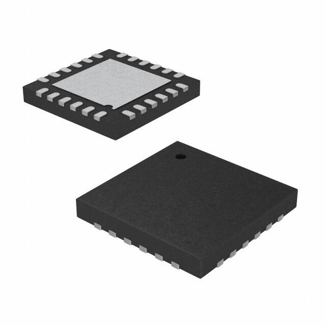
24-pin QFN package
■
Commercial and industrial temperature ranges
Benefits
■
Wide operating output frequency range
❐ 3 to 166 MHz
■
Serial programmable over 2-wire I2C interface
■
Programmable spread spectrum with center and down
spread option and Lexmark and Linear modulation profiles
■
VDD supply voltage options:
❐ 2.5V, 3.0V, and 3.3V for CY2545
❐ 1.8V for CY2547
■
■
Selectable output clock voltages independent of VDD supply:
❐ 2.5V, 3.0V, and 3.3V for CY2545
❐ 1.8V for CY2547
■
Power down, output enable, or frequency select features
■
Low jitter, high accuracy outputs
■
Ability to synthesize nonstandard frequencies with
Fractional-N capability
■
Up to eight clock outputs with programmable drive strength
■
Multiple high performance PLLs allow synthesis of unrelated
frequencies
■
Nonvolatile programming for personalization of PLL
frequencies, spread spectrum characteristics, drive strength,
crystal load capacitance, and output frequencies
■
Application specific programmable EMI reduction using
Spread Spectrum for clocks
■
Programmable PLLs for system frequency margin tests
■
Meets critical timing requirements in complex system
designs
■
Suitability for PC, consumer, portable, and networking applications
■
Capable of Zero PPM frequency synthesis error
■
Uninterrupted system operation during clock frequency
switch
■
Application compatibility in standard and low power systems
Logic Block Diagram
CLKIN/RST
Crossbar
XIN/
EXCLKIN
XOUT
CLK1
Switch
Output
OSC
Bank
1
CLK2
PLL1
Dividers
CLK3
and
Drive
PLL2
MUX
and
Control
Logic
FS
Bank
2
CLK5
Strength
Control
CLK6
Bank
3
PLL3
(SS)
CLK4
CLK7
CLK8
SCL
SDA
PLL4
(SS)
I2C
PD#/OE
SSON
Cypress Semiconductor Corporation
Document #: 001-13196 Rev. *A
•
198 Champion Court
•
San Jose, CA 95134-1709
•
408-943-2600
Revised October 05, 2007
[+] Feedback
�CY2545
CY2547
Pinouts
XIN/
EXCLKIN
XOUT
VDD
CLKIN/RST
CLK8
GND
Figure 1. Pin Diagram - CY2545 24 LD QFN
24
23
22
21
20
19
GND
1
18
GND
CLK1
2
17
CLK7
VDD_CLK_B1
3
16
VDD_CLK_B3
CY2545
24LD QFN
DNU
5
14
VDD_CLK_B2
6
13
CLK5
8
9
10
11
12
GND
7
CLK4
CLK2
CLK3/FS
CLK6/SSON
SDA
15
SCL
4
GND
PD#OE
Table 1. Pin Definition - CY2545 24 LD QFN (VDD = 2.5V, 3.0V or 3.3V Supply)
Pin Number
Name
IO
Description
1
GND
Power
Power supply ground
2
CLK1
Output
Programmable clock output. Output voltage depends on Bank1 voltage
3
VDD_CLK_B1
Power
Power supply for Bank1 (CLK1, CLK2) output: 2.5V/3.0V/3.3V
4
PD#/OE
Input
Multifunction programmable pin: Output enable or Power down mode
5
DNU
DNU
Do not use this pin
6
CLK2
Output
Programmable clock output. Output voltage depends on Bank1 voltage
7
GND
Power
Power supply ground
8
SCL
Input
Serial data clock
9
SDA
Input/Output
Serial data input/output
10
CLK3/FS
Output/Input
Multifunction programmable pin: Programmable clock output or frequency
select input pin. Output voltage of CLK3 depends on Bank2 voltage
11
CLK4
Output
Programmable clock output. Output voltage depends on Bank2 voltage
12
GND
Power
Power supply ground
13
CLK5
Output
Programmable clock output. Output voltage depends on Bank2 voltage
14
VDD_CLK_B2
Power
Power supply for Bank2 (CLK3, CLK4, CLK5) output: 2.5V/3.0V/3.3V
15
CLK6/SSON
Output/Input
Multifunction programmable pin: Programmable clock output or spread
spectrum ON/OFF control input pin. Output voltage of CLK6 depends on
Bank3 voltage
16
VDD_CLK_B3
Power
Power supply for Bank3 (CLK6, CLK7, CLK8) output: 2.5V/3.0V/3.3V
17
CLK7
Output
Programmable clock output. Output voltage depends on Bank3 voltage
18
GND
Power
Power supply ground
19
GND
Power
Power supply ground
20
CLK8
Output
Programmable clock output. Output voltage depends on Bank3 voltage
21
CLKIN/RST
Input/Input
Multifunction programmable pin. High true reset input or 2.5V/3.0V/3.3V
external reference clock input. The signal level of CLKIN input must track
VDD power supply on pin 22.
Document #: 001-13196 Rev. *A
Page 2 of 15
[+] Feedback
�CY2545
CY2547
Table 1. Pin Definition - CY2545 24 LD QFN (VDD = 2.5V, 3.0V or 3.3V Supply) (continued)
Pin Number
Name
IO
Description
22
VDD
Power
Power supply for core and inputs: 2.5V/3.0V/3.3V
23
XOUT
Output
Crystal output
24
XIN/EXCLKIN
Input
Crystal input or 1.8V external clock input
GND
22
CLK8
23
CLKIN/RST
XOUT
24
VDD
XIN/
EXCLKIN
Figure 2. Pin Diagram - CY2547 24 LD QFN
21
20
19
GND
1
18
GND
CLK1
2
17
CLK7
VDD_CLK_B1
3
16
VDD_CLK_B3
CY2547
24LD QFN
CLK6/SSON
VDD
5
14
VDD_CLK_B2
CLK2
6
13
CLK5
10
11
12
GND
9
CLK4
8
CLK3/FS
7
SDA
15
SCL
4
GND
PD#OE
Table 2. Pin Definition - CY2547 24 LD QFN (VDD = 1.8V Supply)
Pin Number
Name
IO
Description
1
GND
Power
Power supply ground
2
CLK1
Output
Programmable clock output. Output voltage depends on Bank1 voltage
3
VDD_CLK_B1
Power
Power supply for Bank1 (CLK1, CLK2) output: 1.8V
4
PD#/OE
Input
Multifunction programmable pin: Output enable or Power down mode
5
VDD
Power
Power supply for core and inputs: 1.8V
6
CLK2
Output
Programmable output clock. Output voltage depends on Bank1 voltage
7
GND
Power
Power supply ground
8
SCL
Input
Serial data clock
9
SDA
Input/Output
Serial data input
10
CLK3/FS
Output/Input
Multifunction programmable pin: Programmable clock output or frequency
select input pin. Output voltage of CLK3 depends on VDD_CLK_B2 voltage
11
CLK4
Output
Programmable output clock. Output voltage depends on Bank2 voltage
12
GND
Power
Power supply ground
13
CLK5
Output
Programmable clock output. Output voltage depends on Bank2 voltage
14
VDD_CLK_B2
Power
Power supply for Bank2 (CLK3, CLK4, CLK5) output: 1.8V
15
CLK6/SSON
Output/Input
Multifunction programmable pin: Programmable clock output or spread
spectrum ON/OFF control input pin. Output voltage of CLK6 depends on
VDD_CLK_B3 voltage
16
VDD_CLK_B3
Power
Power supply for Bank3 (CLK6, CLK7, CLK8) output: 1.8V
17
CLK7
Output
Programmable clock output. Output voltage depends on Bank3 voltage
18
GND
Power
Power supply ground
Document #: 001-13196 Rev. *A
Page 3 of 15
[+] Feedback
�CY2545
CY2547
Table 2. Pin Definition - CY2547 24 LD QFN (VDD = 1.8V Supply) (continued)
Pin Number
Name
IO
Description
19
GND
Power
Power supply ground
20
CLK8
Output
Programmable clock output. Output voltage depends on Bank3 voltage
21
CLKIN/RST
Input/Input
Multifunction programmable pin: High true reset input or 1.8V external low
voltage reference clock input
22
VDD
Power
Power supply for core and inputs: 1.8V
23
XOUT
Output
Crystal output
24
XIN/EXCLKIN
Input
Crystal input or 1.8V external clock input
General Description
Four Configurable PLLs
Output Source Selection
2
The CY2545 and CY2547 have four I C programmable PLLs
available to generate output frequencies ranging from 3 to 166
MHz. The advantage of having four PLLs is that a single device
generates up to four independent frequencies from a single
crystal. Two sets of frequencies for each PLL can be
programmed. This enables in system frequency switching using
multifunction frequency select pin, FS.
These devices have eight clock outputs (CLK1 - 8). There are six
available clock sources for these outputs. These clock sources
are: XIN/EXCLKIN, CLKIN, PLL1, PLL2, PLL3, or PLL4. Output
clock source selection is done using four out of six crossbar
switch. Thus, any one of these six available clock sources can
be arbitrarily selected for the clock outputs. This gives user a
flexibility to have up to four independent clock outputs.
I2C Programming
Spread Spectrum Control
I 2C
The CY2545 and CY2547 have a serial
interface that
programs the configuration memory array to synthesize output
frequencies by programmable output divider, spread characteristics, drive strength, and crystal load capacitance. I2C can also
be used for in system control of these programmable features.
Input Reference Clocks
The input to the CY2545 and CY2547 is either a crystal or a clock
signal. The input frequency range for crystals is 8 MHz to 48
MHz. There is provision for two reference clock inputs, CLKIN
and EXCLKIN with frequency range of 8 MHz to 166 MHz. For
both devices, when CLKIN signal at pin 21 is used as a reference
input, a valid signal at EXCLKIN (as specified in the AC and DC
Electrical Specification table), must be present for the devices to
operate properly.
Multiple Power Supplies
The CY2545 and CY2547 are designed to operate at internal
core supply voltage of 1.8V. In the case of the high voltage part
(CY2545), an internal regulator is used to generate 1.8V from the
2.5V/3.0V/3.3V VDD supply voltage at pin 22. For the low voltage
part (CY2547), this internal regulator is bypassed and 1.8V at
VDD pin 22 is directly used.
Output Bank Settings
These devices have eight clock outputs grouped in three output
driver banks. The Bank 1, Bank 2, and Bank 3 correspond to
(CLK1, CLK2), (CLK3, CLK4, CLK5), and (CLK6, CLK7, CLK8),
respectively. Separate power supplies are used for each of these
banks and they can be any of 2.5V, 3.0V, or 3.3V for CY2545 and
1.8V for CY2547 giving user multiple choice of output clock
voltage levels.
Document #: 001-13196 Rev. *A
Two of the four PLLs (PLL3 and PLL4) have spread spectrum
capability for EMI reduction in the system. The device uses a
Cypress proprietary PLL and Spread Spectrum Clock (SSC)
technology to synthesize and modulate the frequency of the PLL.
The spread spectrum feature can be turned on or off using a
multifunction control pin (CLK7/SSON). It can be programmed to
either center spread range from ±0.125% to ±2.50% or down
spread range from –0.25% to –5.0% with Lexmark or Linear
profile.
Frequency Select
The device can store two different PLL frequency configurations,
output source selection and output divider values for all eight
outputs in its nonvolatile memory location. There is a multifunction programmable pin, CLK3/FS which, if programmed as
frequency select input, can be used to select between these two
arbitrarily programmed settings.
Glitch-Free Frequency Switch
When the frequency select pin (FS) is used to switch frequency,
the outputs are glitch-free provided frequency is switched using
output dividers. This feature enables uninterrupted system
operation while clock frequency is switched.
Device Reset Function
There is a multifunction CLKIN/RST (pin 21) that can be
programmed to use for the device reset function. There are two
different programmable modes of operation for this device reset
function. First one (called POR like reset), when used brings the
device in the default register settings loosing all configuration
changes made through the I2C interface. The second (called
Clean Start), keeps the I2C programmed values while giving all
outputs a simultaneous clean start from its low pull down state.
Page 4 of 15
[+] Feedback
�CY2545
CY2547
PD#/OE Mode
Output Drive Strength
PD#/OE (Pin 4) is programmable to operate as either power
down (PD#) or output enable (OE) mode. PD# is a low true input.
If activated it shuts off the entire chip, resulting in minimum
device power consumption. Setting this signal high brings the
device into operational mode with default register settings.
The DC drive strength of the individual clock output can be
programmed for different values. Table 3 shows the typical rise
and fall times for different drive strength settings.
When this pin is programmed as output enable (OE), clock
outputs are enabled or disabled using OE pin. Individual clock
outputs can be programmed to be sensitive to this OE pin.
Table 3. Output Drive Strength
Output Drive Strength
Rise/Fall Time (ns)
(Typical Value)
Low
6.8
Keep Alive Mode
Mid Low
3.4
By activating the device in the keep alive mode, power down
mode is changed to power saving mode. This disables all PLLs
and outputs, but preserves the contents of the volatile registers.
Thus, any configuration changes made through the I2C interface
are preserved. By deactivating the keep alive mode, I2C memory
is not preserved during power down, but power consumption is
reduced relative to the keep alive mode.
Mid High
2.0
High
1.0
Document #: 001-13196 Rev. *A
Generic Configuration and Custom Frequency
There is a generic set of output frequencies available from the
factory that can be used for the device evaluation purposes. The
device, CY2545/CY2547 can be custom programmed to any
desired frequencies and listed features. For customer specific
programming and I2C programmable memory bitmap definitions,
please contact your local Cypress Field Application Engineer
(FAE) or sales representative.
Page 5 of 15
[+] Feedback
�CY2545
CY2547
Serial I2C Programming Interface Protocol
and Timing
To enhance the flexibility and function of the clock synthesizer, a
two signal serial interface is provided. Through the Serial Data
Interface, various device functions, such as individual clock
output buffers, are individually enabled or disabled. The registers
associated with the Serial Data Interface initialize to their default
setting upon power up and therefore, use of this interface is
optional. Clock device register changes are normally made at
system initialization, if any are required.
The CY2545 and CY2547 use a 2-wire serial interface SDA and
SCL that operates up to 400 kbits/s in read or write mode. The
SDA and SCL timing and data transfer sequence is shown in
Figure 3. The basic write serial format is:
eight bits must contain the data word intended for storage. After
the data word is received, the slave responds with another
acknowledge bit (ack = 0/LOW), and the master must end the
write sequence with a STOP condition.
Writing Multiple Bytes
To write multiple bytes at a time, the master does not end the
write sequence with a STOP condition; instead, the master
sends multiple contiguous bytes of data to be stored. After each
byte, the slave responds with an acknowledge bit, the same as
after the first byte, and accepts data until the STOP condition
responds to the acknowledge bit. When receiving multiple bytes,
the CY2545 and CY2547 internally increment the register
address.
Read Operations
Start Bit; 7-bit Device Address (DA); R/W Bit; Slave Clock
Acknowledge (ACK); 8-bit Memory Address (MA); ACK; 8-bit
Data; ACK; 8-bit Data in MA+1 if desired; ACK; 8-bit Data in
MA+2; ACK; etc. until STOP Bit. The basic serial format is illustrated in Figure 4.
Read operations are initiated the same way as write operations
except that the R/W bit of the slave address is set to ‘1’ (HIGH).
There are three basic read operations: current address read,
random read, and sequential read.
Device Address
Current Address Read
The device serial interface address is 69H. The device address
is combined with a read/write bit as the LSB and is sent after
each start bit.
The CY2545 and CY2547 have an onboard address counter that
retains 1 more than the address of the last word access. If the
last word written or read was word ‘n’, then a current address
read operation returns the value stored in location ‘n+1’. When
the CY2545/CY2547 receive the slave address with the R/W bit
set to a ‘1’, the CY2545/CY2547 issue an acknowledge and
transmit the 8-bit word. The master device does not
acknowledge the transfer, but generates a STOP condition,
which causes the CY2545/CY2547 to stop transmission.
Data Valid
Data is valid when the clock is HIGH, and is only transitioned
when the clock is LOW, as illustrated in Figure 5.
Data Frame
A start and stop sequence indicates every new data frame, as
illustrated in Figure 6.
Start Sequence - The start frame is indicated by SDA going LOW
when SCL is HIGH. Every time a start signal is supplied, the next
8-bit data must be the device address (seven bits) and a R/W bit,
followed by register address (eight bits) and register data (eight
bits).
Stop Sequence - The stop frame is indicated by SDA going HIGH
when SCL is HIGH. A stop frame frees the bus to go to another
part on the same bus or to another random register address.
Acknowledge Pulse
During write mode the CY2545/CY2547 responds with an
acknowledge pulse after every eight bits. Do this by pulling the
SDA line LOW during the N*9th clock cycle as illustrated in
Figure 7 (N = the number of bytes transmitted). During read
mode, the master generates the acknowledge pulse after
reading the data packet.
Write Operations
Writing Individual Bytes
A valid write operation must have a full 8-bit register address
after the device address word from the master, which is followed
by an acknowledge bit from the slave (ack = 0/LOW). The next
Document #: 001-13196 Rev. *A
Random Read
Through random read operations, the master may access any
memory location. To perform this type of read operation, first the
word address must be set. This is done by sending the address
to the CY2545/CY2547 as part of a write operation. After sending
the word address, the master generates a START condition
following the acknowledge. This terminates the write operation
before any data is stored in the address, but not before the
internal address pointer is set. Next, the master reissues the
control byte with the R/W byte set to ‘1’. The CY2545/CY2547
then issue an acknowledge and transmit the 8-bit word. The
master device does not acknowledge the transfer, but generates
a STOP condition, which causes the CY2545/CY2547 to stop
transmission.
Sequential Read
Sequential read operations follow the same process as random
reads except that the master issues an acknowledge instead of
a STOP condition after transmitting the first 8-bit data word. This
action increments the internal address pointer, and subsequently
output of the next 8-bit data word. By continuing to issue
acknowledges instead of STOP conditions, the master serially
reads the entire contents of the slave device memory. When the
internal address pointer points to the FFH register, after the next
increment, the pointer points to the 00H register.
Page 6 of 15
[+] Feedback
�CY2545
CY2547
Figure 3. Data Transfer Sequence on the Serial Bus
SCL
SDA
Address or
Acknowledge
Valid
START
Condition
STOP
Condition
Data may
be changed
Figure 4. Data Frame Architecture
SDA Write
Multiple
Contiguous
Registers
1 Bit
1 Bit Slave
R/W = 0 ACK
7-bit
Device
Address
1 Bit
Slave
ACK
8-bit
Register
Address
(XXH)
1 Bit
Slave
ACK
8-bit
Register
Data
(XXH)
1 Bit
Slave
ACK
8-bit
Register
Data
(XXH+1)
1 Bit
Slave
ACK
8-bit
Register
Data
(XXH+2)
1 Bit
Slave
ACK
8-bit
Register
Data
(FFH)
1 Bit
Slave
ACK
8-bit
Register
Data
(00H)
Stop Signal
Start Signal
SDA Read
Current
Address
Read Start Signal
SDA Read
Multiple
Contiguous
Registers
1 Bit
Slave
ACK
1 Bit
1 Bit Slave
R/W = 1 ACK
7-bit
Device
Address
1 Bit
Slave
ACK
1 Bit
Master
ACK
8-bit
Register
Data
Stop Signal
1 Bit
1 Bit Slave
ACK
R/W = 0
7-bit
Device
Address
1 Bit
Slave
ACK
8-bit
Register
Address
(XXH)
1 Bit
Master
ACK
7-bit
Device
Address
+R/W=1
1 Bit
Master
ACK
8-bit
Register
Data
(XXH)
1 Bit
Master
ACK
8-bit
Register
Data
(XXH+1)
8-bit
Register
Data
(FFH)
1 Bit
Master
ACK
1 Bit
Master
ACK
1 Bit
Master
ACK
8-bit
Register
Data
(00H)
Stop Signal
Start Signal
Repeated
Start bit
Figure 5. Data Valid and Data Transition Periods
Data Valid
Transition
to next Bit
SDA
tDH
tSU
CLKHIGH
VIH
SCL
Document #: 001-13196 Rev. *A
VIL
CLKLOW
Page 7 of 15
[+] Feedback
�CY2545
CY2547
Serial I2C Programming Interface Timing
Figure 6. .Start and Stop Frame
SDA
Transition
to next Bit
START
SCL
STOP
Figure 7. Frame Format (Device Address, R/W, Register Address, Register Data)
SDA
+
START
SCL
DA6
DA5 DA0
+
R/W
ACK
RA7
RA6 RA1
+
RA0
ACK
+
+
D7
D6
D1
D0
ACK
STOP
+
Serial I2C Programming Interface Timing Specifications
Parameter
fSCL
Description
Frequency of SCL
Min
Max
Unit
–
400
kHz
Start Mode Time from SDA LOW to SCL LOW
0.6
–
μs
CLKLOW
SCL LOW Period
1.3
–
μs
CLKHIGH
SCL HIGH Period
0.6
–
μs
tSU
Data Transition to SCL HIGH
250
–
ns
tDH
Data Hold (SCL LOW to data transition)
0
–
ns
Rise Time of SCL and SDA
–
300
ns
Fall Time of SCL and SDA
–
300
ns
Stop Mode Time from SCL HIGH to SDA HIGH
0.6
–
µs
Stop Mode to Start Mode
1.3
–
µs
Document #: 001-13196 Rev. *A
Page 8 of 15
[+] Feedback
�CY2545
CY2547
Absolute Maximum Conditions
Min
Max
Unit
VDD
Parameter
Supply voltage for CY2545
Description
Condition
–0.5
4.5
V
VDD
Supply Voltage for CY2547
–0.5
2.6
V
VDD_CLK_BX
Output Bank supply voltage
–0.5
4.5
V
VIN
Input voltage for CY2545
Relative to VSS
–0.5
VDD+0.5
V
VIN
Input voltage for CY2547
Relative to VSS
–0.5
2.2
V
+150
TS
Temperature and storage
Nonfunctional
–65
ESDHBM
ESD protection (Human Body Model)
JEDEC EIA/JESD22-A114-E
2000
UL-94
Flammability rating
V-0 @1/8 in.
MSL
Moisture sensitivity level
°C
Volts
10
ppm
3
Recommended Operating Conditions
Min
Typ
Max
Unit
VDD
Parameter
VDD Operating voltage for CY2545
Description
2.25
–
3.60
V
VDD
VDD Operating voltage for CY2547
1.65
1.8
1.95
V
VDD_CLK_BX
Output driver voltage for Bank 1, 2 and 3
1.43
–
3.60
V
TAC
Commercial ambient temperature
TAI
Industrial ambient temperature
CLOAD
Maximum load capacitance
tPU
Power up time for all VDD to reach minimum specified voltage (power
ramps must be monotonic)
Document #: 001-13196 Rev. *A
0
–
+70
°C
–40
--
+85
°C
–
–
15
pF
0.05
–
500
ms
Page 9 of 15
[+] Feedback
�CY2545
CY2547
DC Electrical Specifications
Parameter
VOL
Description
Output low voltage
Conditions
IOL = 2 mA, drive strength = [00]
Min
Typ
Max
Unit
–
–
0.4
V
VDD_CLK_BX
– 0.4
–
–
V
IOL = 3 mA, drive strength = [01]
IOL = 7 mA, drive strength = [10]
IOL = 12 mA, drive strength = [11]
VOH
Output high voltage
IOH = –2 mA, drive strength = [00]
IOH = –3 mA, drive strength = [01]
IOH = –7 mA, drive strength = [10]
IOH = –12 mA, drive strength = [11]
VOLSD
Output low voltage, SDA
–
–
0.4
V
VIL1
Input low voltage of PD#/OE,
RST, FS, and SSON
–
–
0.2*VDD
V
VIL2
Input low voltage of CLKIN for
CY2545
–
–
0.1*VDD
V
VIL3
Input low voltage of EXCLKIN for
CY2545
–
–
0.18
V
VIL4
Input low voltage of CLKIN,
EXCLKIN for CY2547
–
–
0.1*VDD
V
VIH1
Input high voltage of PD#/OE,
RST, FS, and SSON
0.8*VDD
–
–
V
VIH2
Input high voltage of CLKIN for
CY2545
0.9*VDD
–
–
V
VIH3
Input high voltage of EXCLKIN
for CY2545
1.62
–
2.2
V
VIH4
Input high voltage of CLKIN,
EXCLKIN for CY2547
0.9*VDD
–
–
V
IILPD
Input low current of RST and
PD#/OE
VIL = 0V
–
–
10
µA
IIHPD
Input high current of RST and
PD#/OE
VIH = VDD
–
–
10
µA
IILSR
Input low current of SSON and
FS
VIL = 0V (Internal pull dn = 160k typ)
–
–
10
µA
IIHSR
Input high current of SSON and VIH = VDD (Internal pull dn = 160k typ)
FS
14
–
36
µA
RDN
Pull down resistor of
(CLK1-CLK8) when off,
CLK6/SSON and CLK3/FS
100
160
250
kΩ
IDD[1,2]
Supply current for CY2547
PD# = High, No load
–
20
–
mA
Supply current for CY2545
PD# = High, No load
–
22
–
mA
[1]
IOL = 4 mA
2
IDDS
Standby current
PD# = Low, No load, with I C circuit not
in Keep Alive Mode
–
3
–
µA
IPD[1]
Power down current
PD# = Low, No load, with I2C circuit in
Keep Alive Mode
–
–
1
mA
CIN[1]
Input capacitance
SSON, RST, PD#/OE or FS inputs
–
7
pF
Document #: 001-13196 Rev. *A
Page 10 of 15
[+] Feedback
�CY2545
CY2547
AC Electrical Specifications
Parameter
Description
FIN (crystal)
Crystal frequency, XIN
Conditions
Min
Typ
Max
Unit
8
–
48
MHz
8
–
166
MHz
3
–
166
MHz
FIN (clock)
Input clock frequency
FCLK
Output clock frequency
DC1
Output duty cycle, all clocks
except Ref Out
Duty cycle is defined in Figure 9; t1/t2, measured 50%
of VDD
45
50
55
%
DC2
Clock inputs CLKIN or EXCLKIN
Ref out clock duty cycle
Ref In Min 45%, Max 55%
40
–
60
%
[1]
Output rise/fall time
Measured from 20% to 80% of VDD_CLK_BX, as shown
in Figure 10, CLOAD = 15 pF, Drive strength [00]
–
6.8
–
ns
TRF2[1]
Output rise/fall time
Measured from 20% to 80% of VDD_CLK_BX, as shown
in Figure 10, CLOAD = 15 pF, Drive strength [01]
–
3.4
–
ns
TRF3[1]
Output rise/fall time
Measured from 20% to 80% of VDD_CLK_BX, as shown
in Figure 10, CLOAD = 15 pF, Drive strength [10]
–
2.0
–
ns
TRF4[1]
Output rise/fall time
Measured from 20% to 80% of VDD_CLK_BX, as shown
in Figure 10, CLOAD = 15 pF, Drive strength [11]
–
1.0
–
ns
TCCJ[1,2]
Cycle-to-cycle jitter max (Pk-Pk)
Configuration dependent. See Table 4
–
150
–
ps
PLL Lock time
Measured from 90% of the applied power supply level
–
1
3
ms
TRF1
[1]
TLOCK
Table 4. Configuration Example for C-C Jitter
Ref. Freq.
(MHz)
CLK1 Output
CLK2 Output
CLK3 Output
CLK4 Output
CLK5 Output
Freq.
(MHz)
C-C Jitter
Typ (ps)
Freq.
(MHz)
C-C Jitter
Typ (ps)
Freq.
(MHz)
C-C Jitter
Typ (ps)
Freq.
(MHz)
C-C Jitter
Typ (ps)
14.3181
8.0
134
166
103
48
92
74.25
81
19.2
74.25
99
166
94
8
91
27
110
27
48
67
27
109
166
103
74.25
97
48
48
93
27
123
166
137
166
138
Freq.
(MHz)
C-C Jitter
Typ (ps)
Not Used
48
75
Not Used
8
103
Recommended Crystal Specification for SMD Package
Parameter
Description
Range 1
Range 2 Range 3
Unit
Fmin
Minimum frequency
8
14
28
MHz
Fmax
Maximum frequency
14
28
48
MHz
R1
Motional resistance (ESR)
135
50
30
Ω
C0
Shunt capacitance
4
4
2
pF
CL
Parallel load capacitance
18
14
12
pF
DL(max)
Maximum crystal drive level
300
300
300
µW
Recommended Crystal Specification for Thru-Hole Package
Parameter
Fmin
Description
Minimum frequency
Range 1
8
Range 2 Range 3
14
Unit
24
MHz
Fmax
Maximum frequency
14
24
32
MHz
R1
Motional resistance (ESR)
90
50
30
Ω
C0
Shunt capacitance
7
7
7
pF
CL
Parallel load capacitance
18
12
12
pF
DL(max)
Maximum crystal drive level
1000
1000
1000
µW
Notes
1. Guaranteed by design but not 100% tested.
2. Configuration dependent.
Document #: 001-13196 Rev. *A
Page 11 of 15
[+] Feedback
�CY2545
CY2547
Test and Measurement Setup
Figure 8. Test and Measurement Setup
V DD
0.1 μF
Outputs
C LOAD
DUT
GND
Voltage and Timing Definitions
Figure 9. Duty Cycle Definition
t1
t2
VDD_CLK_BX
50% of V
Clock
Output
DD_CLK_BX
0V
Figure 10. Rise Time = TRF, Fall Time = TRF
TRF
TRF
V DD_CLK_BX
80% of V
Clock
Output
Document #: 001-13196 Rev. *A
20% of V
DD_CLK_BX
DD_CLK_BX
0V
Page 12 of 15
[+] Feedback
�CY2545
CY2547
Ordering Information
Part Number[1]
Type
VDD(V)
Production Flow
Pb-free
CY2545Cxxx
24-pin QFN
Supply voltage: 2.5V, 3.0V or 3.3V
Commercial, 0°C to 70°C
CY2545CxxxT
24-pin QFN Tape & Reel Supply voltage: 2.5V, 3.0V or 3.3V
Commercial, 0°C to 70°C
CY2547Cxxx
24-pin QFN
Supply voltage: 1.8V
Commercial, 0°C to 70°C
CY2547CxxxT
24-pin QFN Tape & Reel Supply voltage: 1.8V
Commercial, 0°C to 70°C
CY2545Ixxx
24-pin QFN
Industrial, –40°C to 85°C
Supply voltage: 2.5V, 3.0V or 3.3V
CY2545IxxxT
24-pin QFN Tape & Reel Supply voltage: 2.5V, 3.0V or 3.3V
Industrial, –40°C to 85°C
CY2547Ixxx
24-pin QFN
Supply voltage: 1.8V
Industrial, –40°C to 85°C
CY2547IxxxT
24-pin QFN Tape & Reel Supply voltage: 1.8V
Industrial, –40°C to 85°C
Note
1. xxx indicates Factory Programmable and are factory programmed configurations. For more details, contact your local Cypress FAE or Cypress Sales Representative.
Document #: 001-13196 Rev. *A
Page 13 of 15
[+] Feedback
�CY2545
CY2547
Package Drawing and Dimensions
Figure 11. 24-LD QFN 4x4 mm (Subcon Punch Type Pkg with 2.49x2.49 EPAD) LF24A/LY24A
SIDE VIEW
TOP VIEW
BOTTOM VIEW
0.05
3.90
4.10
1.00 MAX.
0.23±0.05
0.05 MAX.
3.70
3.80
?0.50
C
0.80 MAX.
PIN1 ID
0.20 R.
2.49
0.20 REF.
N
N
1
2
2.45
2.55
3.90
4.10
3.70
3.80
1
2
2.49
0.45
SOLDERABLE
EXPOSED
PAD
0.30-0.50
0.42±0.18
(4X)
0°-12°
C
SEATING
PLANE
0.50
2.45
2.55
NOTES:
1.
HATCH IS SOLDERABLE EXPOSED METAL.
2. REFERENCE JEDEC#: MO-220
51-85203-*A
3. PACKAGE WEIGHT: 0.042g
4. ALL DIMENSIONS ARE IN MM [MIN/MAX]
5. PACKAGE CODE
PART #
DESCRIPTION
LF24A
LY24A
STANDARD
LEAD FREE
Document #: 001-13196 Rev. *A
Page 14 of 15
[+] Feedback
�CY2545
CY2547
Document History Page
Document Title: CY2545 CY2547 Quad PLL Programmable Spread Spectrum Clock Generator with Serial I2C Interface
Document Number: 001-13196
REV.
ECN NO.
Issue
Date
Orig. of
Change
Description of Change
**
870780
See ECN
RGL/AESA New Data Sheet
*A
1504843
See ECN
RGL/AESA Changed I2C Tsu specification from 100ns to 250 ns
Changed ESD spec from MIL-STD to JEDEC
Combined VDD operating condition spec for CY2545 to a single VDD spec
Changed name from VDD_CORE to VDD
© Cypress Semiconductor Corporation, 2007. The information contained herein is subject to change without notice. Cypress Semiconductor Corporation assumes no responsibility for the use of any
circuitry other than circuitry embodied in a Cypress product. Nor does it convey or imply any license under patent or other rights. Cypress products are not warranted nor intended to be used for medical,
life support, life saving, critical control or safety applications, unless pursuant to an express written agreement with Cypress. Furthermore, Cypress does not authorize its products for use as critical
components in life-support systems where a malfunction or failure may reasonably be expected to result in significant injury to the user. The inclusion of Cypress products in life-support systems
application implies that the manufacturer assumes all risk of such use and in doing so indemnifies Cypress against all charges.
Any Source Code (software and/or firmware) is owned by Cypress Semiconductor Corporation (Cypress) and is protected by and subject to worldwide patent protection (United States and foreign),
United States copyright laws and international treaty provisions. Cypress hereby grants to licensee a personal, non-exclusive, non-transferable license to copy, use, modify, create derivative works of,
and compile the Cypress Source Code and derivative works for the sole purpose of creating custom software and or firmware in support of licensee product to be used only in conjunction with a Cypress
integrated circuit as specified in the applicable agreement. Any reproduction, modification, translation, compilation, or representation of this Source Code except as specified above is prohibited without
the express written permission of Cypress.
Disclaimer: CYPRESS MAKES NO WARRANTY OF ANY KIND, EXPRESS OR IMPLIED, WITH REGARD TO THIS MATERIAL, INCLUDING, BUT NOT LIMITED TO, THE IMPLIED WARRANTIES
OF MERCHANTABILITY AND FITNESS FOR A PARTICULAR PURPOSE. Cypress reserves the right to make changes without further notice to the materials described herein. Cypress does not
assume any liability arising out of the application or use of any product or circuit described herein. Cypress does not authorize its products for use as critical components in life-support systems where
a malfunction or failure may reasonably be expected to result in significant injury to the user. The inclusion of Cypress’ product in a life-support systems application implies that the manufacturer
assumes all risk of such use and in doing so indemnifies Cypress against all charges.
Use may be limited by and subject to the applicable Cypress software license agreement.
Document #: 001-13196 Rev. *A
Revised October 05, 2007
Page 15 of 15
Purchase of I2C components from Cypress or one of its sublicensed Associated Companies conveys a license under the Philips I2C Patent Rights to use these components in an I2C system, provided
that the system conforms to the I2C Standard Specification as defined by Philips. All products and company names mentioned in this document may be the trademarks of their respective holders.
[+] Feedback
�


 工商网监
湘ICP备2023018690号
工商网监
湘ICP备2023018690号
