CY25702
Programmable High-Frequency Crystal Oscillator (XO)
Features
•
•
•
•
•
•
•
•
•
•
Benefits
Programmable High-frequency Crystal Oscillator (XO)
Wide operating output clock frequency range of 1–166 MHz
Integrated phase-locked loop (PLL)
85 ps typical cycle-to-cycle Jitter with CLK = 133 MHz
3.3V operation
Output Enable and Power-down functions
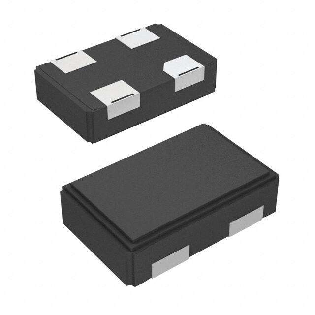
Package available in 4-Pin Ceramic LCC SMD
Pb-free package
Industrial Temperature from –40°C to 85°C
For SSCG functionality refer to CY25701 data sheet
• Internal PLL to generate up to 166 MHz output
• Suitable for most PC, consumer, and networking
applications
• Application compatibility in standard and low-power
systems
• CY25701 can be used as a direct replacement without any
PCB modification if spread spectrum clock (SSC) is required
for EMI reduction.
• In-house programming of samples and prototype quantities
is available using CY3672 programming kit and CY3724
socket adapters. Production quantities are available
through Cypress’s value-added distribution partners or by
using third-party programmers from BP Microsystems, HiLo
Systems, and others.
Pin Configuration
Logic Block Diagram
CY25702
RFB
4-pin Ceramic SMD
PLL
4
VDD
3
CLK
CXIN
PROGRAMMABLE
CONFIGURATION
CXOUT
OUTPUT
DIVIDERS
and
MUX
3
OE/PD#
1
VSS
2
CLK
1
OE/PD#
4
2
VDD
VSS
Cypress Semiconductor Corporation
Document #: 38-07721 Rev. *C
•
198 Champion Court
•
San Jose, CA 95134-1709
•
408-943-2600
Revised December 07, 2006
�CY25702
Pin Definition
Pin
1
Name
Description
OE/PD#
Output Enable pin: Active HIGH. If OE = 1, CLK is enabled.
Power Down pin: Active LOW. If PD# = 0, Power Down is enabled.
2
VSS
Power supply ground.
3
CLK
Clock output.
4
VDD
3.3V power supply.
Table 1. Programming Data Requirement
Pin Function
Output Frequency
Output Enable/Power Down
Pin Name
CLK
OE/PD#
Pin#
3
1
Units
MHz
N/A
Program Value
ENTER DATA
ENTER DATA
Functional Description
Output Frequency, CLK Output (CLK, pin 3)
The CY25702 is a programmable high-frequency Crystal
Oscillator (XO) that uses a Cypress proprietary PLL to
synthesize the frequency of the embedded input crystal.
The CY25702 uses a programmable configuration memory
array to synthesize output frequency. The frequency CLK
output can be programmed from 1 MHz to 166 MHz.
The frequency at the CLK output is produced by synthesizing
the embedded crystal oscillator frequency input. The range of
the synthesized clock is from 1 MHz to 166 MHz.
Output Enable or Power Down (OE/PD#, pin 1)
Pin 1 can be programmed as either output enable (OE) or
Power Down (PD#).
The CY25702 is available in a 4-pin ceramic SMD package
with an operating temperature range of –40 to 85°C.
Absolute Maximum Rating
Programming Description
Supply Voltage (VDD)......................................–0.5V to +7.0V
DC Input Voltage ................................... –0.5V to VDD + 0.5V
Field/Factory-Programmable CY25702
Field/Factory programming is available for samples and
manufacturing by Cypress and its distributors. All requests
must be submitted to the local Cypress Field Application
Engineer (FAE) or sales representative. Once the request has
been processed, you will receive a new part number, samples,
and data sheet with the programmed values. This part number
will be used for additional sample requests and production
orders.
Storage Temperature (Non-condensing) ...... –55°C to 100°C
Junction Temperature .................................. –40°C to 125°C
Data Retention @ Tj = 125°C................................> 10 years
Package Power Dissipation...................................... 350 mW
Additional information on the CY25702 can be obtained from
the Cypress web site at www.cypress.com.
Operating Conditions
Min.
Typ.
Max.
Unit
VDD
Parameter
Supply Voltage
Description
3.00
3.30
3.60
V
TA
Ambient Temperature (Commercial)
–20
–
70
°C
TA
Ambient Temperature (Industrial)
–40
–
85
°C
CLOAD
Max. Load Capacitance @ pin 3
–
–
15
pF
FCLK
CLK output frequency, CLOAD = 15 pF
1
–
166
MHz
TPU
Power-up time for VDD to reach minimum specified voltage (power ramp must be
monotonic)
0.05
–
500
ms
Document #: 38-07721 Rev. *C
Page 2 of 6
�CY25702
DC Electrical Characteristics
Parameter
Description
Condition
Min.
Typ.
Max.
Unit
IOH
Output High Current (pin 3)
VOH = VDD – 0.5, VDD = 3.3V (source)
10
12
–
mA
IOL
Output Low Current (pin 3)
VOL = 0.5, VDD = 3.3V (sink)
10
12
–
mA
VIH
Input High Voltage (pin 1)
CMOS levels, 70% of VDD
0.7VDD
–
VDD
V
VIL
Input Low Voltage (pin 1)
CMOS levels, 30% of VDD
–
–
0.3VDD
V
IIH
Input High Current (pin 1)
Vin = VDD
–
–
10
μA
IIL
Input Low Current (pin 1)
Vin = VSS
–
–
10
μA
IOZ
Output Leakage Current (pin 3)
Three-state output, OE = 0
–10
–
10
μA
CIN[1]
Input Capacitance (pin 1)
Pin 1, or OE
–
5
7
pF
IVDD
Supply Current
VDD = 3.3V, CLK = 1 to 166 MHz,
CLOAD = 0, OE = VDD
–
–
50
mA
Δf/f
Initial Accuracy at Room Temp.
TA = 25°C, 3.3V
–25
–
25
ppm
Freq. Stability over Temp. Range TA = –20°C to 70°C, 3.3V
–25
–
25
ppm
Freq. Stability over Voltage Range 3.0 to 3.6V
–12
–
12
ppm
Aging
–5
–
5
ppm
TA = 25°C, First year
AC Electrical Characteristics[1]
Min.
Typ.
Max.
Unit
DC
Parameter
Output Duty Cycle
Description
CLK, Measured at VDD/2
Condition
45
50
55
%
tR
Output Rise Time
20%–80% of VDD, CL=15 pF
–
–
2.7
ns
tF
Output Fall Time
20%–80% of VDD, CL=15 pF
–
–
2.7
ns
TCCJ1[2]
Cycle-to-Cycle Jitter CLK (Pin 3)
CLK > 133 MHz, Measured at VDD/2
–
85
200
ps
25 MHz < CLK < 133 MHz, Measured at VDD/2
–
215
400
ps
CLK < 25 MHz, Measured at VDD/2
–
–
500
ps
TOE1
Output Disable Time (pin1 = OE)
Time from falling edge on OE to stopped
outputs (Asynchronous)
–
150
350
ns
TOE2
Output Enable Time (pin1 = OE)
Time from rising edge on OE to outputs at a
valid frequency (Asynchronous)
–
150
350
ns
TLOCK
PLL Lock Time
Time for CLK to reach valid frequency
–
–
10
ms
Note
1. Guaranteed by characterization, not 100% tested.
2. Jitter is configuration dependent. Actual jitter is dependent on output frequencies, spread percentage, temperature, and output load. For more information, refer
to the application note, “Jitter in PLL Based Systems: Causes, Effects, and Solutions” available at http://www.cypress.com/clock/appnotes.html, or contact your
local Cypress Field Application Engineer.
Document #: 38-07721 Rev. *C
Page 3 of 6
�CY25702
Application Circuit
Figure 1. Application Circuit Diagram
0 .1 µ F
Pow er
3
4
CLK
VDD
C Y25702
VSS
O E /P D #
1
2
VDD
Switching Waveforms
Figure 2. Duty Cycle Waveform
Cycle Timing (DC = t1A/t1B)
t1A
CLK
t1B
Figure 3. Output Rise/Fall Time Waveform
VDD
CLK
0V
Tr
Tf
Output Rise time (Tr) = (0.6 x VDD)/SR1 (or SR3)
Output Fall time (Tf) = (0.6 x VDD)/SR2 (or SR4)
Refer to AC Electrical Characteristics table for SR (Slew Rate) values.
Figure 4. Output Enable/Disable Timing Waveforms
OUTPUT
ENABLE
VDD
0V
VIH
VIL
TOE2
High Impedance
CLK
(Asynchronous)
TOE1
Document #: 38-07721 Rev. *C
Page 4 of 6
�CY25702
Ordering Information
Part Number
Package Description
Product Flow
Lead-free (Pb-free)
CY25702FLXCT[3]
4-Lead Ceramic LCC SMD -Tape and Reel
Commercial, –20° to 70°C
CY25702FLXIT[3]
4-Lead Ceramic LCC SMD -Tape and Reel
Industrial, –40° to 85°C
CY25702LXCZZZT[4]
4-Lead Ceramic LCC SMD -Tape and Reel
Commercial, –20° to 70°C
CY25702LXIZZZT[4]
4-Lead Ceramic LCC SMD -Tape and Reel
Industrial, –40° to 85°C
Actual Marking[5]
CY25702FLX*
CY25702LX*
F=Field
Programmable
Marketing Part Number (CY25702)
C Y
2
X
*
L
Pin 1 mark L = LCC X = Pb free
5
7
L = LCC
F
C
Y
2
5
7
0
Y W W
X
*
z
z
z
Y W W
0
2
YWW = Date Code (Year & WW)
Temp
Marketing Part Number (CY25702)
Pin 1 mark X = Pb free
Temp
2 L
zzz = Programmable Dash Code YWW = Date Code (Year & WW)
Package Drawings and Dimensions
Figure 5. 4-Lead (5.0x3.2 mm) Ceramic LCC LZ04A
Dimensions in MM
General Tolerance: ± 0.15MM
Kyocera dwg ref KD-VA5G08
Package Weight ~ 0.12 grams
0.50
1.30 Max
SIDE VIEW
5.0
1.20
0.80
#3
#2
3.2
#4
#1
2.90
2.50
TOP VIEW
BOTTOM VIEW
001-02743-*B
All product and company names mentioned in this document are the trademarks of their respective holders.
Notes
3. “FLX” suffix is used for products programmed in field by Cypress Distributors.
4. “ZZZ” denotes the assigned product dash number. This number will be assigned by factory after the output frequency programming data is received from the
customer.
5. Temp can be C (Commercial) or I (Industrial).
Document #: 38-07721 Rev. *C
Page 5 of 6
© Cypress Semiconductor Corporation, 2006. The information contained herein is subject to change without notice. Cypress Semiconductor Corporation assumes no responsibility for the use
of any circuitry other than circuitry embodied in a Cypress product. Nor does it convey or imply any license under patent or other rights. Cypress products are not warranted nor intended to be
used for medical, life support, life saving, critical control or safety applications, unless pursuant to an express written agreement with Cypress. Furthermore, Cypress does not authorize its
products for use as critical components in life-support systems where a malfunction or failure may reasonably be expected to result in significant injury to the user. The inclusion of Cypress
products in life-support systems application implies that the manufacturer assumes all risk of such use and in doing so indemnifies Cypress against all charges.
�CY25702
Document History Page
Document Title: CY25702 Programmable High-Frequency Crystal Oscillator (XO)
Document Number: 38-07721
REV.
ECN NO.
Issue Date
Orig. of
Change
Description of Change
**
296081
See ECN
RGL
New data sheet
*A
333298
See ECN
RGL
Added Jitter Specifications
Corrected the Ordering Information table to match the DevMaster
*B
390406
See ECN
RGL
Removed CY25702FXC and CY25702XCZZZ
*C
595857
See ECN
RGL
Complete data sheet rewrite
Document #: 38-07721 Rev. *C
Page 6 of 6
�


 工商网监
湘ICP备2023018690号
工商网监
湘ICP备2023018690号
