PRELIMINARY
CY28346-2
Clock Synthesizer with Differential CPU Outputs
Features
• Compliant with Intel® CK 408 Mobile Clock Synthesizer specifications • 3.3V power supply • 3 differential CPU clocks • 10 copies of PCI clocks • 5/6 copies of 3V66 clocks • SMBus support with Read Back capabilities Table 1. Frequency Table[1] S2 1 1 1 1 0 0 0 0 M M S1 0 0 1 1 0 0 1 1 0 0 S0 0 1 0 1 0 1 0 1 0 1 CPU (0:2) 66M 100M 200M 133M 66M 100M 200M 133M Hi-Z TCLK/2 3V66 66M 66M 66M 66M 66M 66M 66M 66M Hi-Z TCLK/4 66BUFF(0:2)/ 3V66(0:4) 66IN 66IN 66IN 66IN 66M 66M 66M 66M Hi-Z TCLK/4 66IN/ 3V66-5 66-MHz clock input 66-MHz clock input 66-MHz clock input 66-MHz clock input 66M 66M 66M 66M Hi-Z TCLK/4 PCIF/PCI 66IN/2 66IN/2 66IN/2 66IN/2 33 M 33 M 33 M 33 M Hi-Z TCLK/8 REF 14.318M 14.318M 14.318M 14.318M 14.318M 14.318M 14.318M 14.318M Hi-Z TCLK USB/ DOT 48M 48M 48M 48M 48M 48M 48M 48M Hi-Z TCLK/2 • Spread Spectrum electromagnetic interference (EMI) reduction • Dial-a-Frequency features • Dial-a-dB™ features • Extended operating temperature range, 0°C to 85°C • 56-pin TSSOP packages
Block Diagram
XIN XOUT PLL1 CPU_STP# IREF VSSIREF S(0:2) MULT0 VTT_PWRGD# PCI_STP# PLL2 WD Logic I2C Logic Power Up Logic
/2
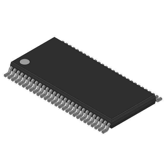
Pin Configuration
REF CPUT(0:2) CPUC(0:2)
VDD XIN XOUT VSS PCIF0 PCIF1 PCIF2 VDD VSS PCI0 PCI1 PCI2 PCI3 VDD VSS PCI4 PCI5 PCI6 VDD VSS 66B0/3V66_2 66B1/3V66_3 66B2/3V66_4 66IN/3V66_5 PD# VDDA VSSA VTT_PWRGD# 1 2 3 4 5 6 7 8 9 10 11 12 13 14 15 16 17 18 19 20 21 22 23 24 25 26 27 28 56 55 54 53 52 51 50 49 48 47 46 45 44 43 42 41 40 39 38 37 36 35 34 33 32 31 30 29 REF S1 S0 CPU_STP# CPUT0 CPUC0 VDD CPUT1 CPUC1 VSS VDD CPUT2 CPUC2 MULT0 IREF VSSIREF S2 48M_USB 48M_DOT VDD VSS 3V66_1/VCH PCI_STP# 3V66_0 VDD VSS SCLK SDATA
3V66_0 3V66_1/VCH PCI(0:6) PCI_F(0:2) 48M_USB 48M_DOT
CY28346-2
PD# SDATA SCLK VDDA
66B[0:2]/3V66[2:4] 66IN/3V66-5
Note: 1. TCLK is a test clock driven on the XTAL_IN input during test mode. M = driven to a level between 1.0V and 1.8V. If the S2 pin is at a M level during power-up, a 0 state will be latched into the devices internal state register.
Cypress Semiconductor Corporation Document #: 38-07509 Rev. *B
•
3901 North First Street
•
San Jose, CA 95134 • 408-943-2600 Revised March 11, 2005
�PRELIMINARY
Pin Description
Pin 2 3 XIN XOUT Name PWR VDD VDD VDD VDDP VDD I/O I O O O O Description
CY28346-2
Oscillator Buffer Input. Connect to a crystal or to an external clock. Oscillator Buffer Output. Connect to a crystal. Do not connect when an external clock is applied at XIN. Differential host output clock pairs. See Table 1 for frequencies and functionality. PCI clock outputs. Are synchronous to 66IN or 3V66 clock. See Table 1. 33-MHz PCI clocks, which are ÷2 copies of 66IN or 3V66 clocks, may be free running (not stopped when PCI_STP# is asserted LOW) or may be stoppable depending on the programming of SMBus register Byte3, Bits (3:5). Buffered output copy of the device’s XIN clock. Current reference programming input for CPU buffers. A resistor is connected between this pin and VSSIREF. Qualifying input that latches S(0:2) and MULT0. When this input is at a logic low, the S(0:2) and MULT0 are latched. Fixed 48-MHz USB clock outputs. Fixed 48-MHZ DOT clock outputs. 3.3V 66-MHz fixed frequency clock. 3.3V clock selectable with SMBus byte0, Bit5, when Byte5, Bit5. When Byte 0 Bit 5 is at a logic 1, then this pin is a 48M output clock. When byte0, Bit5 is a logic 0, then this is a 66M output clock (default). This pin is a power-down mode pin. A logic LOW level causes the device to enter a power-down state. All internal logic is turned off except for the SMBus logic. All output buffers are stopped. Programming input selection for CPU clock current multiplier. Frequency select inputs. See Table 1 Serial data input. Conforms to the SMBus specification of a Slave Receive/Transmit device. It is an input when receiving data. It is an open drain output when acknowledging or transmitting data. Serial clock input. Conforms to the SMBus specification. Frequency select input. See Table 1. This is a Tri-level input that is driven HIGH, LOW, or driven to a intermediate level. PCI clock disable input. When asserted LOW, PCI (0:6) clocks are synchronously disabled in a LOW state. This pin does not effect PCIF (0:2) clocks’ outputs if they are programmed to be PCIF clocks via the device’s SMBus interface. CPU clock disable input. When asserted LOW, CPUT (0:2) clocks are synchronously disabled in a HIGH state and CPUC(0:2) clocks are synchronously disabled in a LOW state. Input connection for 66CLK(0:2) output clock buffers if S2 = 1, or output clock for fixed 66-MHz clock if S2 = 0. See Table 1. 3.3V clock outputs. These clocks are buffered copies of the 66IN clock or fixed at 66 MHz. See Table 1.
52, 51, 49, 48, CPUT(0:2), 45, 44 CPUC(0:2) 10, 11, 12, 13, PCI(0:6) 16, 17, 18 5, 6, 7 PCIF (0:2)
56 42 28 39 38 33 35
REF IREF VTT_PWRGD# 48M_USB 48M_DOT 3V66_0 3V66_1/VCH
VDD VDD VDD VDD48 VDD48 VDD VDD
O I I O O O O
25
PD#
VDD
I PU I PU I I
43 55, 54 29
MULT0 S(0,1) SDATA
VDD I I
30 40 34
SCLK S2 PCI_STP#
I VDD VDD
I I T I PU
53
CPU_STP#
VDD
I PU I/O O
24 21, 22, 23
66IN/3V66_5 66B(0:2)/ 3V66(2:4)
VDD VDD – –
1, 8, 14, 19, 32, VDD 37, 46, 50 4, 9, 15, 20, 27, VSS 31, 36, 47
PWR 3.3V power supply. PWR Common ground.
Document #: 38-07509 Rev. *B
Page 2 of 20
�PRELIMINARY
Pin Description (continued)
Pin 41 Name VSSIREF PWR – I/O Description
CY28346-2
PWR Current reference programming input for CPU buffers. A resistor is connected between this pin and IREF. This pin should also be returned to device VSS. PWR Analog power input. Used for PLL and internal analog circuits. It is also specifically used to detect and determine when power is at an acceptable level to enable the device to operate.
26
VDDA
–
Serial Data Interface
To enhance the flexibility and function of the clock synthesizer, a two-signal serial interface is provided. Through the Serial Data Interface, various device functions, such as individual clock output buffers, can be individually enabled or disabled. The registers associated with the Serial Data Interface initializes to their default setting upon power-up, and therefore use of this interface is optional. Clock device register changes are normally made upon system initialization, if any are required. The interface can also be used during system operation for power management functions. Table 2. Block Read and Block Write Protocol Block Write Protocol Bit 1 2:8 9 10 11:18 19 20:27 28 29:36 37 38:45 46 .... .... .... .... .... .... Start Slave address – 7 bits Write = 0 Acknowledge from slave Command Code – 8 bit ‘00000000’ stands for block operation Acknowledge from slave Byte Count – 8 bits Acknowledge from slave Data byte 1 – 8 bits Acknowledge from slave Data byte 2 – 8 bits Acknowledge from slave ...................... Data Byte (N–1) –8 bits Acknowledge from slave Data Byte N –8 bits Acknowledge from slave Stop Description
Data Protocol
The clock driver serial protocol accepts block write and block read operations from the controller. For block write/read operation, the bytes must be accessed in sequential order from lowest to highest byte (most significant bit first) with the ability to stop after any complete byte has been transferred. The block write and block read protocol is outlined in Table 2. The slave receiver address is 11010010 (D2h).
Block Read Protocol Bit 1 2:8 9 10 11:18 19 20 21:27 28 29 30:37 38 39:46 47 48:55 56 .... .... .... .... Start Slave address – 7 bits Write = 0 Acknowledge from slave Command Code – 8 bit ‘00000000’ stands for block operation Acknowledge from slave Repeat start Slave address – 7 bits Read = 1 Acknowledge from slave Byte count from slave – 8 bits Acknowledge Data byte from slave – 8 bits Acknowledge Data byte from slave – 8 bits Acknowledge Data bytes from slave/Acknowledge Data byte N from slave – 8 bits Not Acknowledge Stop Description
Document #: 38-07509 Rev. *B
Page 3 of 20
�PRELIMINARY
Byte 0: CPU Clock Register Bit @Pup 7 6 0 0 3V66_1/VCH CPUT,CPUC PCI Name Description
CY28346-2
Spread Spectrum Enable, 0 = Spread Off, 1 = Spread On. This is a Read and Write control bit. CPU clock Power-down Mode Select. 0 = Drive CPUT(0:2) to 4 or 6 IREF and drive CPUC(0:2) to low when PD# is asserted LOW. 1 = Three-state all CPU outputs. This is only applicable when PD# is LOW. It is not applicable to CPU_STP#. 3V66_1/VCH frequency Select, 0 = 66M selected, 1 = 48M selected This is a Read and Write control bit. CPU_STP#. Reflects the current value of the external CPU_STP# (pin 53) This bit is Read-only. Reflects the current value of the internal PCI_STP# function when read. Internally PCI_STP# is a logical AND function of the internal SMBus register bit and the external PCI_STP# pin. Frequency Select Bit 2. Reflects the value of SEL2 (pin 40). This bit is Read-only. Frequency Select Bit 1. Reflects the value of SEL1 (pin 55). This bit is Read-only. Frequency Select Bit 0. Reflects the value of SEL0 (pin 54). This bit is Read-only. Name MULT0 Description MULT0 (Pin 43) Value. This bit is Read-only.
5 4 3 2 1 0
0 Pin 53 Pin 34 Pin 40 Pin 55 Pin 54
Byte 1: CPU Clock Register Bit @Pup 7 6 Pin 43 0
Controls functionality of CPUT/C(0:2) outputs when CPU_STP# is asserted. 0 = Drive CPUT(0:2) to 4 or 6 IREF and drive CPUC(0:2) to low when CPU_STP# asserted LOW. 1 = Three-state all CPU CPU_STP# outputs. This bit will override Byte0, Bit6 such that even if it is a 0, when PD# goes low the CPU outputs will be three-stated. CPUT2 CPUC2 CPUT1 CPUC1 CPUT0 CPUC0 CPUT2 CPUC2 CPUT1 CPUC1 CPUT0 CPUC0 Controls CPU2 functionality when CPU_STP# is asserted LOW 1 = Free Running, 0 = Stopped LOW with CPU_STP# asserted LOW This is a Read and Write control bit. Controls CPU1 functionality when CPU_STP# is asserted LOW 1 = Free Running, 0 = Stopped LOW with CPU_STP# asserted LOW This is a Read and Write control bit. Controls CPUT0 functionality when CPU_STP# is asserted LOW 1 = Free Running, 0 = Stopped LOW with CPU_STP# asserted LOW This is a Read and Write control bit. CPUT/C2 Output Control, 1 = enabled, 0 = disable HIGH and CPUC2 disables LOW This is a Read and Write control bit. CPUT/C1 Output Control, 1 = enabled, 0 = disable HIGH and CPUC1 disables LOW This is a Read and Write control bit. CPUT/C0 Output Control, 1 = enabled, 0 = disable HIGH and CPUC0 disables LOW This is a Read and Write control bit.
5
0
4
0
3 2 1 0
0 1 1 1
Byte 2: PCI Clock Control Register (all bits are read and write functional) Bit 7 6 5 4 3 2 1 0 @Pup 0 1 1 1 1 1 1 1 Name REF PCI6 PCI5 PCI4 PCI3 PCI2 PCI1 PCI0 Description REF Output Control. 0 = high strength, 1 = low strength PCI6 Output Control. 1 = enabled, 0 = forced LOW PCI5 Output Control. 1 = enabled, 0 = forced LOW PCI4 Output Control. 1 = enabled, 0 = forced LOW PCI3 Output Control. 1 = enabled, 0 = forced LOW PCI2 Output Control. 1 = enabled, 0 = forced LOW PCI1 Output Control. 1 = enabled, 0 = forced LOW PCI0 Output Control. 1 = enabled, 0 = forced LOW
Document #: 38-07509 Rev. *B
Page 4 of 20
�PRELIMINARY
Byte 3: PCIF Clock and 48M Control Register (all bits are read and write functional) Bit 7 6 5 4 3 2 1 0 @Pup 1 1 0 0 0 1 1 1 Name 48M_DOT 48M_USB PCIF2 PCIF1 PCIF0 PCIF2 PCIF1 PCIF0 Description
CY28346-2
48M_DOT Output Control,1 = enabled, 0 = forced LOW 48M_USB Output Control,1 = enabled, 0 = forced LOW PCI_STP#, control of PCIF2. 0 = Free Running, 1 = Stopped when PCI_STP# is LOW PCI_STP#, control of PCIF1. 0 = Free Running, 1 = Stopped when PCI_STP# is LOW PCI_STP#, control of PCIF0. 0 = Free Running, 1 = Stopped when PCI_STP# is LOW PCIF2 Output Control. 1=running, 0=forced LOW PCIF1 Output Control. 1= running, 0=forced LOW PCIF0 Output Control. 1= running, 0=forced LOW
Byte 4: DRCG Control Register(all bits are read and write functional) Bit 7 6 5 4 3 2 1 0 @Pup 0 0 1 1 1 1 1 1 3V66_0 3V66_1/VCH 3V66_5 66B2/3V66_4 66B1/3V66_3 66B0/3V66_2 Name Reserved 3V66_0 Output Enabled. 1 = enabled, 0 = disabled 3V66_1/VCH Output Enable. 1 = enabled, 0 = disabled 3V66_5 Output Enable. 1 = enabled, 0 = disabled 66B2/3V66_4 Output Enabled. 1 = enabled, 0 = disabled 66B1/3V66_3 Output Enabled. 1 = enabled, 0 = disabled 66B0/3V66_2 Output Enabled. 1 = enabled, 0 = disabled Description SS2 Spread Spectrum control bit (0 = down spread, 1 = center spread)
Byte 5: Clock Control Register (all bits are read and write functional) Bit 7 6 5 4 3 2 1 0 @Pup 0 1 0 0 0 0 0 0 Name Description SS1 Spread Spectrum control bit SS0 Spread Spectrum control bit 66IN to 66M delay Control MSB 66IN to 66M delay Control LSB Reserved 48M_DOT edge rate control. When set to 1, the edge is slowed by 15%. Reserved USB edge rate control. When set to 1, the edge is slowed by 15%
Byte 6: Silicon Signature Register[2] (all bits are read-only) Bit 7 6 5 4 3 2 1 0 @Pup 0 0 0 1 0 0 1 1 Vendor Code, 011 = IMI Name Description
Note: 2. When writing to this register the device will acknowledge the write operation, but the data itself will be ignored.
Document #: 38-07509 Rev. *B
Page 5 of 20
�PRELIMINARY
Byte 7: Watchdog Time Stamp Register Bit 7 6 5 4 3 2 1 0 @Pup 0 0 0 0 0 0 0 0 Name Reserved Reserved Reserved Reserved Reserved Reserved Reserved Reserved Description
CY28346-2
Byte 8: Dial-a-Frequency Control Register N (all bits are read and write functional) Bit 7 6 5 4 3 2 1 0 Bit 7 6 5 4 3 2 1 0 @Pup 0 0 0 0 0 0 0 0 @Pup 0 0 0 0 0 0 0 0 Name R6 MSB R5 R4 R3 R2 R1 R0, LSB R and N register load gate 0 = gate closed (data is latched), 1 = gate open (data is loading from SMBus registers into R and N) Name N7, MSB N6 N5 N4 N3 N2 N3 N0, LSB Description Description
Byte 9: Dial-a-Frequency Control Register R (all bits are read and write functional)
Dial-a-Frequency Feature
SMBus Dial-a-Frequency feature is available in this device via Byte8 and Byte9. See our App Note AN-0025 for details on our Dial-a-Frequency feature. P is a large value PLL constant that depends on the frequency selection achieved through the hardware selectors (S1, S0). P value may be determined from Table 3. Table 3. P Value S(1:0) 00 01 10 11 P 32005333 48008000 96016000 64010667
Dial-a-dB Features
SMBus Dial-a-dB feature is available in this device via Byte8 and Byte9.
Spread Spectrum Clock Generation (SSCG)
Spread Spectrum is a modulation technique used to minimizing EMI radiation generated by repetitive digital signals. A clock presents the greatest EMI energy at the center frequency it is generating. Spread Spectrum distributes this energy over a specific and controlled frequency bandwidth therefore causing the average energy at any one point in this band to decrease in value. This technique is achieved by modulating the clock away from its resting frequency by a certain percentage (which also determines the amount of EMI reduction). In this device, Spread Spectrum is enabled by setting specific register bits in the SMBus control Bytes. Table 4 is a listing of the modes and percentages of Spread Spectrum modulation that this device incorporates. Page 6 of 20
Document #: 38-07509 Rev. *B
�PRELIMINARY
Table 4. Spread Spectrum SS2 0 0 0 0 1 1 1 1 SS1 0 0 1 1 0 0 1 1 SS0 0 1 0 1 0 1 0 1 Spread Mode Down Down Down Down Center Center Center Center Spread% +0.00, –0.25 +0.00, –0.50 +0.00, –0.75 +0.00, –1.00 +0.13, –0.13 +0.25, –0.25 +0.37, –0.37 +0.50, –1.50
CY28346-2
Configured as VCH (48M), SMBus Byte0, Bit 5 = ‘1’ In this mode, the output is configured as a 48-MHz non-spread spectrum output. This output is phase aligned with the other 48M outputs (USB and DOT), to within 1 ns pin-to-pin skew. The switching of 3V66_1/VCH into VCH mode occurs at system power on. When the SMBus Bit 5 of Byte 0 is programmed from a ‘0’ to a ‘1’, the 3V66_1/VCH output may glitch while transitioning to 48M output mode. PD# (Power-down) Clarification The PD# (Power-down) pin is used to shut off ALL clocks prior to shutting off power to the device. PD# is an asynchronous active LOW input. This signal is synchronized internally to the device powering down the clock synthesizer. PD# is an asynchronous function for powering up the system. When PD# is low, all clocks are driven to a LOW value and held there and the VCO and PLLs are also powered down. All clocks are shut down in a synchronous manner so has not to cause glitches while transitioning to the low ‘stopped’ state. PD#—Assertion When PD# is sampled LOW by two consecutive rising edges of the CPUC clock, then on the next HIGH-to-LOW transition of PCIF, the PCIF clock is stopped LOW. On the next HIGH-to-LOW transition of 66Buff, the 66Buff clock is stopped LOW. From this time, each clock will stop LOW on its next HIGH-to-LOW transition, except the CPUT clock. The CPU clocks are held with the CPUT clock pin driven HIGH with a value of 2 x Iref, and CPUC undriven. After the last clock has stopped, the rest of the generator will be shut down.
Special Functions
PCIF and IOAPIC Clock Outputs The PCIF clock outputs are intended to be used, if required, for systems IOAPIC clock functionality. ANY two of the PCIF clock outputs can be used as IOAPIC 33-MHz clock outputs. They are 3.3V outputs will be divided down via a simple resistive voltage divider to meet specific system IOAPIC clock voltage requirements. In the event these clocks are not required, then these clocks can be used as general PCI clocks or disabled via the assertion of the PCI_STP# pin. 3V66_1/VCH Clock Output The 3V66_1/VCH pin has a dual functionality that is selectable via SMBus. Configured as DRCG (66M), SMBus Byte0, Bit 5 = ‘0’ The default condition for this pin is to power up in a 66M operation. In 66M operation this output is SSCG capable and when spreading is turned on, this clock will be modulated.
66Buff PCIF PW RDW N# CPU 133MHz CPU# 133MHz 3V66 66In USB 48MHz REF 14.318MHz
Figure 1. Power-down Assertion Timing Waveforms—Buffered Mode
Document #: 38-07509 Rev. *B
Page 7 of 20
�PRELIMINARY
CY28346-2
PW RDW N# C P U T 133M H z C P U C 133M H z P C I 33M H z A G P 66M H z U S B 48M H z R E F 1 4 .3 1 8 M H z D D R T 133M H z D D R C 133M H z S D R A M 133M H z
Figure 2. Power-down Assertion Timing Waveforms—Unbuffered Mode
PD# Deassertion
The power-up latency between PD# rising to a valid logic ‘1’ level and the starting of all clocks is less than 3.0 ms.
0.25mS
VDDA = 2.0V
Sample Inputs straps
Wait for


 工商网监
湘ICP备2023018690号
工商网监
湘ICP备2023018690号
