CY7B9910
CY7B9920
Low Skew Clock Buffer
Low Skew Clock Buffer
Features
Block Diagram Description
■
All outputs skew < 100 ps typical (250 max)
Phase Frequency Detector and Filter
■
15 to 80 MHz output operation
■
Zero input to output delay
■
50% duty cycle outputs
■
Outputs drive 50 terminated lines
The phase frequency detector and Filter blocks accept inputs
from the reference frequency (REF) input and the feedback (FB)
input and generate correction information to control the
frequency of the voltage controlled oscillator (VCO). These
blocks, along with the VCO, form a phase-locked loop (PLL) that
tracks the incoming REF signal.
■
Low operating current
VCO
■
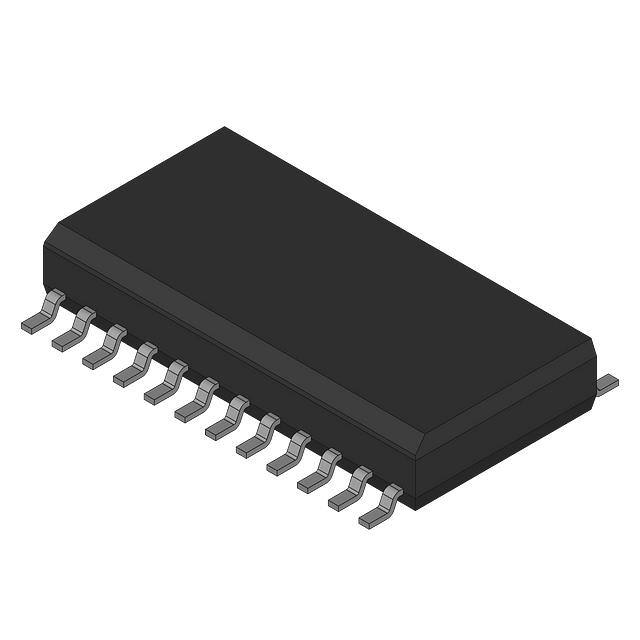
24-pin small-outline integrated circuit (SOIC) package
■
Jitter: < 200 ps peak-to-peak, < 25 ps RMS
The VCO accepts analog control inputs from the PLL filter block
and generates a frequency. The operational range of the VCO is
determined by the FS control pin.
Functional Description
The CY7B9910 and CY7B9920 low skew clock buffers offer low
skew system clock distribution. These multiple output clock
drivers optimize the timing of high performance computer
systems. Each of the eight individual drivers can drive terminated
transmission lines with impedances as low as 50 . They deliver
minimal and specified output skews and full swing logic levels
(CY7B9910 TTL or CY7B9920 CMOS).
The completely integrated PLL enables ‘zero delay’ capability.
External divide capability, combined with the internal PLL, allows
distribution of a low frequency clock that is multiplied by virtually
any factor at the clock destination. This facility minimizes clock
distribution difficulty while allowing maximum system clock
speed and flexibility.
Logic Block Diagram
TEST
FB
Phase
Freq Det
Filter
REF
Voltage
Controlled
Oscillator
FS
Q0
Q1
Q2
Q3
Q4
Q5
Q6
Q7
Cypress Semiconductor Corporation
Document Number: 38-07135 Rev. *F
•
198 Champion Court
•
San Jose, CA 95134-1709
•
408-943-2600
Revised September 6, 2010
[+] Feedback
�CY7B9910
CY7B9920
Contents
Pinouts .............................................................................. 3
Test Mode .......................................................................... 3
Maximum Ratings ............................................................. 4
Operating Range ............................................................... 4
Electrical Characteristics ................................................. 4
Capacitance ...................................................................... 5
Switching Characteristics ................................................ 6
Switching Characteristics ................................................ 7
Switching Characteristics ................................................ 8
AC Timing Diagrams ........................................................ 9
Operational Mode Descriptions .................................... 10
Document Number: 38-07135 Rev. *F
Ordering Information ...................................................... 11
Ordering Code Definition ........................................... 11
Package Diagram ............................................................ 12
Acronyms ........................................................................ 13
Document Conventions ................................................. 13
Units of Measure ....................................................... 13
Document History Page ................................................. 14
Sales, Solutions, and Legal Information ...................... 15
Worldwide Sales and Design Support ....................... 15
Products .................................................................... 15
PSoC Solutions ......................................................... 15
Page 2 of 15
[+] Feedback
�CY7B9910
CY7B9920
Pinouts
Figure 1. Pin Configuration – 24-pin (300-Mil) Molded SOIC
SOIC
Top View
REF
VCCQ
FS
NC
VCCQ
VCCN
Q0
Q1
GND
Q2
Q3
VCCN
1
24
2
23
3
22
4
21
20
5
6
7
7B9910
7B9920
19
18
8
17
9
16
10
15
11
14
12
13
GND
TEST
NC
GND
VCCN
Q7
Q6
GND
Q5
Q4
VCCN
FB
Table 1. Pin Definition
Signal Name
IO
Description
REF[1]
I
Reference frequency input. This input supplies the frequency and timing against which all functional
variations are measured.
FB
I
PLL feedback input (typically connected to one of the eight outputs).
FS[1, 2, 3]
I
Three level frequency range select. The ranges are described in the switching characteristics
tables.
TEST
I
Three level select. See TEST MODE.
O
Clock outputs.
Q[0..7]
NC
NC
No connect.
VCCN
PWR
Power supply for output drivers.
VCCQ
PWR
Power supply for internal circuitry.
GND
PWR
Ground.
Test Mode
The TEST input is a three level input. In normal system operation, this pin is connected to ground, allowing the CY7B9910 and
CY7B9920 to operate as described in Block Diagram Description on page 1. For testing purposes, any of the three level inputs can
have a removable jumper to ground or be tied LOW through a 100 resistor. This enables an external tester to change the state of
these pins.
If the TEST input is forced to its MID or HIGH state, the device operates with its internal phase locked loop disconnected and input
levels supplied to REF directly control all outputs. Relative output-to-output functions are the same as in normal mode.
Notes
1. When the FS pin is selected HIGH, the REF input must not transition upon power up until VCC reached 4.3 V.
2. The level to be set on FS is determined by the “normal” operating frequency (fNOM) of the VCO (see Logic Block Diagram). The frequency appearing at the REF and
FB inputs are fNOM when the output connected to FB is undivided. The frequency of the REF and FB inputs are fNOM / X when the device is configured for a frequency
multiplication by using external division in the feedback path of value X.
3. For all three state inputs, HIGH indicates a connection to VCC, LOW indicates a connection to GND, and MID indicates an open connection. Internal termination
circuitry holds an unconnected input to VCC / 2.
Document Number: 38-07135 Rev. *F
Page 3 of 15
[+] Feedback
�CY7B9910
CY7B9920
Maximum Ratings
Operating Range
Exceeding maximum ratings may shorten the useful life of the
device. User guidelines are not tested.
Range
Ambient
Temperature
Storage temperature ................................ –65 C to +150 C
VCC
Commercial
0 C to +70 C
5 V 10%
Ambient temperature with
power applied ........................................... –55 C to +125 C
Industrial
–40 C to +85 C
5 V 10%
Supply voltage to ground potential ...............–0.5 V to +7.0 V
DC input voltage ...........................................–0.5 V to +7.0 V
Output current into outputs (LOW) .............................. 64 mA
Static discharge voltage........................................... > 2001 V
(MIL-STD-883, method 3015)
Latch-up current ..................................................... > 200 mA
Electrical Characteristics
Over the Operating Range
Parameter
Description
Test Conditions
VCC = Min, IOH = –16 mA
CY7B9910
CY7B9920
Min
Max
Min
Max
Unit
2.4
–
–
–
V
VOH
Output HIGH voltage
VOL
Output LOW voltage
–
VIH
Input HIGH voltage
(REF and FB inputs only)
2.0
VIL
Input LOW voltage
(REF and FB inputs only)
–0.5
VCC = Min, IOH = –40 mA
–
–
VCC – 0.75
–
VCC = Min, IOL = 46 mA
–
0.45
–
–
–
–
0.45
VCC
VCC – 1.35
VCC
V
0.8
–0.5
1.35
V
VCC
VCC – 1 V
VCC
V
VCC / 2 –
500 mV
VCC / 2 +
500 mV
V
VCC = Min, IOL = 46 mA
VIHH
Three level input HIGH
voltage (Test, FS)[4]
Min VCC Max
VCC – 1 V
VIMM
Three level input MID
voltage (Test, FS)[4]
Min VCC Max
VCC / 2 – VCC / 2 +
500 mV 500 mV
VILL
Three level input LOW
voltage (Test, FS)[4]
Min VCC Max
V
0.0
1.0
0.0
1.0
V
–
10
–
10
µA
–500
–
–500
–
µA
–
200
–
200
µA
–50
50
–50
50
µA
IIH
Input HIGH leakage current VCC = Max, VIN = Max
(REF and FB inputs only)
IIL
Input LOW leakage current
(REF and FB inputs only)
VCC = Max, VIN = 0.4 V
IIHH
Input HIGH current
(Test, FS)
VIN = VCC
IIMM
Input MID current
(Test, FS)
VIN = VCC / 2
IILL
Input LOW current
(Test, FS)
VIN = GND
–
–200
–
–200
µA
IOS
Output short circuit
current[5]
VCC = Max, VOUT
= GND (25 C only)
–
–250
–
N/A
mA
Notes
4. These inputs are normally wired to VCC, GND, or left unconnected (actual threshold voltages vary as a percentage of VCC). Internal termination resistors hold
unconnected inputs at VCC / 2. If these inputs are switched, the function and timing of the outputs may glitch and the PLL may require an additional tLOCK time before
all datasheet limits are achieved.
5. Tested one output at a time, output shorted for less than one second, less than 10% duty cycle. Room temperature only. CY7B9920 outputs are not short circuit
protected.
Document Number: 38-07135 Rev. *F
Page 4 of 15
[+] Feedback
�CY7B9910
CY7B9920
Electrical Characteristics
Over the Operating Range (continued)
Parameter
Description
Operating current used by
internal circuitry
VCCN = VCCQ = Max
All input selects open
ICCN
Output buffer current per
output pair[6]
PD
Power dissipation per
output pair[7]
ICCQ
CY7B9910
Test Conditions
Min
CY7B9920
Max
Min
Max
Unit
mA
Commercial
–
85
–
85
Industrial
–
90
–
90
VCCN = VCCQ = Max
IOUT = 0 mA
Input selects open, fMAX
–
14
–
19
mA
VCCN = VCCQ = Max
IOUT = 0 mA
Input selects open, fMAX
–
78
–
104[8]
mW
Capacitance[9]
Tested initially and after any design or process changes that may affect these parameters.
Parameter
Description
Test Conditions
CIN
Input capacitance
Max
Unit
10
pF
TA = 25 C, f = 1 MHz, VCC = 5.0 V
Figure 2. AC Test Loads and Waveforms
5V
R1
CL
R2
3.0 V
R1 = 130
R2 = 91
CL = 50 pF (CL = 30pF for –5 and – 2 devices)
(Includes fixture and probe capacitance)
7B9910–3
TTL AC Test Load (CY7B9910)
2.0 V
Vth =1.5 V
0.8 V
0.0 V
R1
CL
R2
7B9910–5
CMOS AC Test Load (CY7B9920)
1 ns
1 ns
7B9910–4
TTL Input Test Waveform (CY7B9910)
VCC
R1 = 100
R2 = 100
CL = 50 pF (CL = 30 pF for –5 and –2 devices)
(Includes fixture and probe capacitance)
2.0 V
Vth =1.5 V
0.8 V
VCC
80%
Vth = VCC / 2
20%
0.0 V
3 ns
80%
Vth = VCC / 2
20%
3 ns
7B9910–6
CMOS Input Test Waveform (CY7B9920)
Notes
6. Total output current per output pair is approximated by the following expression that includes device current plus load current:
CY7B9910:
ICCN = [(4 + 0.11 F) + [((835 – 3 F) / Z) + (.0022 FC)] N] x 1.1
CY7B9920:
ICCN = [(3.5 +.17 F) + [((1160 – 2.8 F) / Z) + (.0025 FC)] N] x 1.1
Where
F = frequency in MHz
C = capacitive load in pF
Z = line impedance in ohms
N = number of loaded outputs; 0, 1, or 2
FC = F < C.
7. Total power dissipation per output pair is approximated by the following expression that includes device power dissipation plus power dissipation due to the load circuit:
CY7B9910:
PD = [(22 + 0.61 F) + [((1550 – 2.7 F) / Z) + (.0125 FC)] N] x 1.1
CY7B9920:
PD = [(19.25+ 0.94 F) + [((700 + 6 F) / Z) + (.017 FC)] N] x 1.1.See note 3 for variable definition.
8. CMOS output buffer current and power dissipation specified at 50 MHz reference frequency.
9. Applies to REF and FB inputs only.
Document Number: 38-07135 Rev. *F
Page 5 of 15
[+] Feedback
�CY7B9910
CY7B9920
Switching Characteristics
Over the Operating Range [10]
Parameter
fNOM
tRPWH
tRPWL
tSKEW
tDEV
tPD
tODCV
tORISE
tOFALL
tLOCK
tJR
CY7B9910–2[11]
Min
Typ
Max
Operating clock
FS = LOW[12, 13]
15
–
30
frequency in MHz
FS = MID[12, 13]
25
–
50
[12, 13, 14]
FS = HIGH
40
–
80
REF pulse width HIGH
5.0
–
–
REF pulse width LOW
5.0
–
–
Zero output skew (all outputs)[16, 17]
–
0.1
0.25
Device-to-device skew[17, 18]
–
–
0.75
Propagation delay, REF rise to FB rise
–0.25
0.0
+0.25
Output duty cycle variation[19]
–0.65
0.0
+0.65
Output rise time[20, 21]
0.15
1.0
1.2
[20,
21]
Output fall time
0.15
1.0
1.2
PLL lock time[22]
–
–
0.5
Cycle-to-cycle output jitter Peak-to-peak
–
–
200
RMS
–
–
25
Description
CY7B9920–2[11]
Min
Typ
Max
15
–
30
25
–
50
40
–
80[15]
5.0
–
–
5.0
–
–
–
0.1
0.25
–
–
0.75
–0.25
0.0
+0.25
–0.65
0.0
+0.65
0.5
2.0
2.5
0.5
2.0
2.5
–
–
0.5
–
–
200
–
–
25
Unit
MHz
ns
ns
ns
ns
ns
ns
ns
ns
ms
ps
ps
Notes
10. Test measurement levels for the CY7B9910 are TTL levels (1.5 V to 1.5 V). Test measurement levels for the CY7B9920 are CMOS levels (VCC / 2 to VCC / 2).
Test conditions assume signal transition times of 2 ns or less and output loading as shown in the AC Test Loads and Waveforms unless otherwise specified.
11. Guaranteed by statistical correlation. Tested initially and after any design or process changes that may affect these parameters.
12. For all three state inputs, HIGH indicates a connection to VCC, LOW indicates a connection to GND, and MID indicates an open connection. Internal termination
circuitry holds an unconnected input to VCC / 2.
13. The level to be set on FS is determined by the “normal” operating frequency (fNOM) of the VCO (see Logic Block Diagram). The frequency appearing at the REF
and FB inputs are fNOM when the output connected to FB is undivided. The frequency of the REF and FB inputs are fNOM / X when the device is configured for
a frequency multiplication by using external division in the feedback path of value X.
14. When the FS pin is selected HIGH, the REF input must not transition upon power-up until VCC reached 4.3 V.
15. Except as noted, all CY7B9920–2 and –5 timing parameters are specified to 80 MHz with a 30 pF load.
16. tSKEW is defined as the time between the earliest and the latest output transition among all outputs when all are loaded with 50 pF and terminated with 50 to
2.06 V (CY7B9910) or VCC / 2 (CY7B9920).
17. tSKEW is defined as the skew between outputs.
18. tDEV is the output-to-output skew between any two outputs on separate devices operating under the same conditions (VCC, ambient temperature, air flow, and
so on).
19. tODCV is the deviation of the output from a 50% duty cycle.
20. Specified with outputs loaded with 30 pF for the CY7B99X0–2 and –5 devices and 50 pF for the CY7B99X0–7 devices. Devices are terminated through 50 to
2.06 V (CY7B9910) or VCC / 2 (CY7B9920).
21. tORISE and tOFALL measured between 0.8 V and 2.0 V for the CY7B9910 or 0.8 VCC and 0.2 VCC for the CY7B9920.
22. tLOCK is the time that is required before synchronization is achieved. This specification is valid only after VCC is stable and within normal operating limits. This
parameter is measured from the application of a new signal or frequency at REF or FB until tPD is within specified limits.
Document Number: 38-07135 Rev. *F
Page 6 of 15
[+] Feedback
�CY7B9910
CY7B9920
Switching Characteristics
Over the Operating Range [23]
Parameter
Description
[24, 25]
fNOM
Operating clock
frequency in MHz
FS = LOW
FS = MID[24, 25]
FS = HIGH[24, 25, 26]
tRPWH
tRPWL
tSKEW
tDEV
tPD
tODCV
tORISE
tOFALL
tLOCK
tJR
REF pulse width HIGH
REF pulse width LOW
Zero output skew (All outputs)[28, 29]
Device-to-device skew[30, 31]
Propagation delay, REF rise to FB rise
Output duty cycle variation[32]
Output rise time[33, 34]
Output fall time[33, 34]
PLL lock time[35]
Cycle-to-cycle output jitter Peak-to-peak[30]
RMS[30]
Min
15
25
40
5.0
5.0
–
–
–0.5
–1.0
0.15
0.15
–
–
–
CY7B9910–5
Typ
Max
–
30
–
50
–
80
–
–
–
–
0.25
0.5
–
1.0
0.0
+0.5
0.0
+1.0
1.0
1.5
1.0
1.5
–
0.5
–
200
–
25
Min
15
25
40
5.0
5.0
–
–
–0.5
–1.0
0.5
0.5
–
–
–
CY7B9920–5
Typ
Max
–
30
–
50
–
80[27]
–
–
–
–
0.25
0.5
–
1.0
0.0
+0.5
0.0
+1.0
2.0
3.0
2.0
3.0
–
0.5
–
200
–
25
Unit
MHz
ns
ns
ns
ns
ns
ns
ns
ns
ms
ps
ps
Notes
23. Test measurement levels for the CY7B9910 are TTL levels (1.5 V to 1.5 V). Test measurement levels for the CY7B9920 are CMOS levels (VCC / 2 to VCC / 2).
Test conditions assume signal transition times of 2 ns or less and output loading as shown in the AC Test Loads and Waveforms unless otherwise specified.
24. For all three state inputs, HIGH indicates a connection to VCC, LOW indicates a connection to GND, and MID indicates an open connection. Internal termination
circuitry holds an unconnected input to VCC / 2.
25. The level to be set on FS is determined by the “normal” operating frequency (fNOM) of the VCO (see Logic Block Diagram). The frequency appearing at the REF
and FB inputs are fNOM when the output connected to FB is undivided. The frequency of the REF and FB inputs are fNOM / X when the device is configured for
a frequency multiplication by using external division in the feedback path of value X.
26. When the FS pin is selected HIGH, the REF input must not transition upon power up until VCC reached 4.3 V.
27. Except as noted, all CY7B9920–2 and –5 timing parameters are specified to 80 MHz with a 30 pF load.
28. tSKEW is defined as the time between the earliest and the latest output transition among all outputs when all are loaded with 50 pF and terminated with 50 to
2.06 V (CY7B9910) or VCC / 2 (CY7B9920).
29. tSKEW is defined as the skew between outputs.
30. Guaranteed by statistical correlation. Tested initially and after any design or process changes that may affect these parameters.
31. tDEV is the output-to-output skew between any two outputs on separate devices operating under the same conditions (VCC, ambient temperature, air flow, and
so on).
32. tODCV is the deviation of the output from a 50% duty cycle.
33. Specified with outputs loaded with 30 pF for the CY7B99X0–2 and –5 devices and 50 pF for the CY7B99X0–7 devices. Devices are terminated through 50 to
2.06 V (CY7B9910) or VCC / 2 (CY7B9920).
34. tORISE and tOFALL measured between 0.8 V and 2.0 V for the CY7B9910 or 0.8 VCC and 0.2 VCC for the CY7B9920.
35. tLOCK is the time that is required before synchronization is achieved. This specification is valid only after VCC is stable and within normal operating limits. This
parameter is measured from the application of a new signal or frequency at REF or FB until tPD is within specified limits.
Document Number: 38-07135 Rev. *F
Page 7 of 15
[+] Feedback
�CY7B9910
CY7B9920
Switching Characteristics
Over the Operating Range [36]
Parameter
Description
FS = LOW[37, 38]
FS = MID[37, 38]
FS = HIGH[37, 38, 39]
fNOM
Operating clock
frequency in MHz
tRPWH
tRPWL
tSKEW
tDEV
tPD
tODCV
tORISE
tOFALL
tLOCK
tJR
tJR
REF pulse width HIGH
REF pulse width LOW
Zero output skew (All outputs)[41, 42]
Device-to-device skew[43, 44]
Propagation delay, REF Rise to FB Rise
Output duty cycle variation[45]
Output rise time[46, 47]
Output fall time[46, 47]
PLL lock time[48]
Cycle-to-cycle output
Peak-to-peak[43]
jitter
RMS[43]
Min
15
25
40
5.0
5.0
–
–
–0.7
–1.2
0.15
0.15
–
–
–
CY7B9910–7
Typ
Max
–
30
–
50
–
80
–
–
–
–
0.3
0.75
–
1.5
0.0
+0.7
0.0
+1.2
1.5
2.5
1.5
2.5
–
0.5
–
200
–
25
Min
15
25
40
5.0
5.0
–
–
–0.7
–1.2
0.5
0.5
–
–
–
CY7B9920–7
Typ
Max
–
30
–
50
–
80[40]
–
–
–
–
0.3
0.75
–
1.5
0.0
+0.7
0.0
+1.2
3.0
5.0
3.0
5.0
–
0.5
–
200
–
25
Unit
MHz
ns
ns
ns
ns
ns
ns
ns
ns
ms
ps
ps
Notes
36. Test measurement levels for the CY7B9910 are TTL levels (1.5 V to 1.5 V). Test measurement levels for the CY7B9920 are CMOS levels (VCC / 2 to VCC / 2).
Test conditions assume signal transition times of 2 ns or less and output loading as shown in the AC Test Loads and Waveforms unless otherwise specified.
37. For all three state inputs, HIGH indicates a connection to VCC, LOW indicates a connection to GND, and MID indicates an open connection. Internal termination
circuitry holds an unconnected input to VCC / 2.
38. The level to be set on FS is determined by the “normal” operating frequency (fNOM) of the VCO (see Logic Block Diagram). The frequency appearing at the REF
and FB inputs are fNOM when the output connected to FB is undivided. The frequency of the REF and FB inputs are fNOM / X when the device is configured for
a frequency multiplication by using external division in the feedback path of value X.
39. When the FS pin is selected HIGH, the REF input must not transition upon power up until VCC reached 4.3 V.
40. Except as noted, all CY7B9920–2 and –5 timing parameters are specified to 80 MHz with a 30 pF load.
41. tSKEW is defined as the time between the earliest and the latest output transition among all outputs when all are loaded with 50 pF and terminated with 50 to
2.06 V (CY7B9910) or VCC / 2 (CY7B9920).
42. tSKEW is defined as the skew between outputs.
43. Guaranteed by statistical correlation. Tested initially and after any design or process changes that may affect these parameters.
44. tDEV is the output-to-output skew between any two outputs on separate devices operating under the same conditions (VCC, ambient temperature, air flow, and
so on).
45. tODCV is the deviation of the output from a 50% duty cycle.
46. Specified with outputs loaded with 30 pF for the CY7B99X0–2 and –5 devices and 50 pF for the CY7B99X0–7 devices. Devices are terminated through 50
to 2.06 V (CY7B9910) or VCC / 2 (CY7B9920).
47. tORISE and tOFALL measured between 0.8 V and 2.0 V for the CY7B9910 or 0.8 VCC and 0.2 VCC for the CY7B9920.
48. tLOCK is the time that is required before synchronization is achieved. This specification is valid only after VCC is stable and within normal operating limits. This
parameter is measured from the application of a new signal or frequency at REF or FB until tPD is within specified limits.
Document Number: 38-07135 Rev. *F
Page 8 of 15
[+] Feedback
�CY7B9910
CY7B9920
AC Timing Diagrams
Figure 3. AC Timing Diagrams
tREF
t RPWL
t RPWH
REF
tPD
t ODCV
t ODCV
FB
Q
t SKEW
t SKEW
tJR
Other Q
Figure 4. Zero Skew and Zero Delay Clock Driver
REF
Load
Z0
FB
System
Clock
REF
FS
Load
Q0
Q1
Z0
Q2
Q3
Load
Q4
Q5
Z0
Q6
TEST
Q7
Load
Z0
Document Number: 38-07135 Rev. *F
Page 9 of 15
[+] Feedback
�CY7B9910
CY7B9920
Operational Mode Descriptions
Figure 4 on page 9 shows the device configured as a zero skew
clock buffer. In this mode the CY7B9910/CY7B9920 is used as
the basis for a low skew clock distribution tree. The outputs are
aligned and may each drive a terminated transmission line to an
independent load. The FB input is tied to any output and the
operating frequency range is selected with the FS pin. The low
skew specification, coupled with the ability to drive terminated
transmission lines (with impedances as low as 50 ohms),
enables efficient printed circuit board design.
Figure 3 on page 9 shows the CY7B9910/CY7B9920 connected
in series to construct a zero skew clock distribution tree between
boards. Cascaded clock buffers accumulates low frequency jitter
because of the non-ideal filtering characteristics of the PLL filter.
Do not connect more than two clock buffers in series.
Figure 5. Board-to-Board Clock Distribution
REF
Load
Z0
FB
System
Clock
REF
FS
Load
Q0
Q1
Z0
Q2
Q3
Load
Q4
Z0
Q5
Q6
TEST
Q7
FB
REF
FS
Z0
Q0
Q1
Q3
Q4
Q5
TEST
Document Number: 38-07135 Rev. *F
Load
Q2
Load
Q6
Q7
Page 10 of 15
[+] Feedback
�CY7B9910
CY7B9920
Ordering Information
Accuracy
(ps)
500
Pb-free
250
500
750
CY7B9920–5SC[49]
CY7B9920–5SCT[49]
CY7B9920–5SI[49]
24-Pin Small Outline IC
24-Pin Small Outline IC - Tape and Reel
24-Pin Small Outline IC
Operating
Range
Commercial, 0C to +70 C
Commercial, 0C to +70C
Industrial, –40 C to +85 C
CY7B9910–2SXC
CY7B9910–2SXCT
CY7B9910–5SXC
CY7B9910–5SXCT
CY7B9910–5SXI
CY7B9910–5SXIT
CY7B9910–7SXC
CY7B9910–7SXCT
24-Pin Small Outline IC
24-Pin Small Outline IC - Tape and Reel
24-Pin Small Outline IC
24-Pin Small Outline IC - Tape and Reel
24-Pin Small Outline IC
24-Pin Small Outline IC - Tape and Reel
24-Pin Small Outline IC
24-Pin Small Outline IC - Tape and Reel
Commercial, 0 C to +70 C
Commercial, 0 C to +70 C
Commercial, 0 C to +70 C
Commercial, 0 C to +70 C
Industrial, –40 C to +85 C
Industrial, –40 C to +85 C
Commercial, 0C to +70 C
Commercial, 0 C to +70 C
Ordering Code
Package Type
Ordering Code Definition
CY 7B99X0 – X
S
(X) C
(T)
T = Tape and Reel, blank = Tube
Temperature: C = Commercial; I = Industrial
X = Pb-free, blank = not Pb-free
S = SOIC package
Speed grade: 2 / 5 / 7, based on propagation delay
Base part number
7B9910 = Clock buffer with TTL outputs
7B9920 = Clock buffer with CMOS outputs
Company ID: CY = Cypress
Note
49. Not recommended for new design. New designs should use Pb-free devices.
Document Number: 38-07135 Rev. *F
Page 11 of 15
[+] Feedback
�CY7B9910
CY7B9920
Package Diagram
Figure 6. 24-Pin (300-Mil) Molded SOIC
NOTE :
PIN 1 ID
1. JEDEC STD REF MO-119
2. BODY LENGTH DIMENSION DOES NOT INCLUDE MOLD PROTRUSION/END FLASH,BUT
12
DOES INCLUDE MOLD MISMATCH AND ARE MEASURED AT THE MOLD PARTING LINE.
1
MOLD PROTRUSION/END FLASH SHALL NOT EXCEED 0.010 in (0.254 mm) PER SIDE
3. DIMENSIONS IN INCHES
4. PACKAGE WEIGHT 0.65gms
0.291[7.391]
0.300[7.620]
0.394[10.007]
0.419[10.642]
13
24
MIN.
MAX.
*
PART #
S24.3 STANDARD PKG.
SZ24.3 LEAD FREE PKG.
0.026[0.660]
0.032[0.812]
SEATING PLANE
0.597[15.163]
0.615[15.621]
0.092[2.336]
0.105[2.667]
*
0.050[1.270]
TYP.
0.013[0.330]
0.019[0.482]
0.004[0.101]
0.0118[0.299]
0.004[0.101]
0.015[0.381]
0.050[1.270]
0.0091[0.231]
0.0125[0.317]
*
51-85025 *D
Document Number: 38-07135 Rev. *F
Page 12 of 15
[+] Feedback
�CY7B9910
CY7B9920
Acronyms
Acronym
Description
FB
feedback
PLL
phase-locked loop
SOIC
small-outline integrated circuit
VCO
Voltage controlled oscillator
Document Conventions
Units of Measure
Symbol
°C
Unit of Measure
degree Celsius
k
kilohms
MHz
megahertz
µA
microamperes
mA
milliamperes
ms
milliseconds
mW
milliwatts
ns
nanoseconds
ohms
%
percent
pF
picofarads
ppm
parts per million
ps
picoseconds
V
volts
Document Number: 38-07135 Rev. *F
Page 13 of 15
[+] Feedback
�CY7B9910
CY7B9920
Document History Page
Document Title: CY7B9910/CY7B9920 Low Skew Clock Buffer
Document Number: 38-07135
Revision
ECN
Orig. of
Change
Submission Description of Change
Date
**
110244
SZV
10/28/01
Change from Specification number: 38-00437 to 38-07135
*A
1199925
DPF/AESA
See ECN
Added Pb-free parts in Ordering Information
Added Note 20: Not recommended for the new design
*B
1353343
AESA
See ECN
Change status to final
*C
2750166
TSAI
08/10/09
Post to external web
*D
2761988
CXQ
09/10/09
Fixed typo from 100 W resistor to 100 resistor.
Added “Not recommended for new designs” note to Pb devices.
Fixed incorrect instances of auto-replacement of “lead” to “Pb”.
*E
2896073
CXQ
03/19/10
Removed inactive parts from ordering information table
Updated package diagram
*F
3010397
KVM
08/18/2010
Document Number: 38-07135 Rev. *F
Added ordering code definition
Page 14 of 15
[+] Feedback
�CY7B9910
CY7B9920
Sales, Solutions, and Legal Information
Worldwide Sales and Design Support
Cypress maintains a worldwide network of offices, solution centers, manufacturer’s representatives, and distributors. To find the office
closest to you, visit us at Cypress Locations.
Products
Automotive
Clocks & Buffers
Interface
Lighting & Power Control
PSoC Solutions
cypress.com/go/automotive
cypress.com/go/clocks
psoc.cypress.com/solutions
cypress.com/go/interface
PSoC 1 | PSoC 3 | PSoC 5
cypress.com/go/powerpsoc
cypress.com/go/plc
Memory
Optical & Image Sensing
cypress.com/go/memory
cypress.com/go/image
PSoC
cypress.com/go/psoc
Touch Sensing
cypress.com/go/touch
USB Controllers
Wireless/RF
cypress.com/go/USB
cypress.com/go/wireless
© Cypress Semiconductor Corporation, 2001-2010. The information contained herein is subject to change without notice. Cypress Semiconductor Corporation assumes no responsibility for the use of
any circuitry other than circuitry embodied in a Cypress product. Nor does it convey or imply any license under patent or other rights. Cypress products are not warranted nor intended to be used for
medical, life support, life saving, critical control or safety applications, unless pursuant to an express written agreement with Cypress. Furthermore, Cypress does not authorize its products for use as
critical components in life-support systems where a malfunction or failure may reasonably be expected to result in significant injury to the user. The inclusion of Cypress products in life-support systems
application implies that the manufacturer assumes all risk of such use and in doing so indemnifies Cypress against all charges.
Any Source Code (software and/or firmware) is owned by Cypress Semiconductor Corporation (Cypress) and is protected by and subject to worldwide patent protection (United States and foreign),
United States copyright laws and international treaty provisions. Cypress hereby grants to licensee a personal, non-exclusive, non-transferable license to copy, use, modify, create derivative works of,
and compile the Cypress Source Code and derivative works for the sole purpose of creating custom software and or firmware in support of licensee product to be used only in conjunction with a Cypress
integrated circuit as specified in the applicable agreement. Any reproduction, modification, translation, compilation, or representation of this Source Code except as specified above is prohibited without
the express written permission of Cypress.
Disclaimer: CYPRESS MAKES NO WARRANTY OF ANY KIND, EXPRESS OR IMPLIED, WITH REGARD TO THIS MATERIAL, INCLUDING, BUT NOT LIMITED TO, THE IMPLIED WARRANTIES
OF MERCHANTABILITY AND FITNESS FOR A PARTICULAR PURPOSE. Cypress reserves the right to make changes without further notice to the materials described herein. Cypress does not
assume any liability arising out of the application or use of any product or circuit described herein. Cypress does not authorize its products for use as critical components in life-support systems where
a malfunction or failure may reasonably be expected to result in significant injury to the user. The inclusion of Cypress’ product in a life-support systems application implies that the manufacturer
assumes all risk of such use and in doing so indemnifies Cypress against all charges.
Use may be limited by and subject to the applicable Cypress software license agreement.
Document Number: 38-07135 Rev. *F
Revised September 6, 2010
Page 15 of 15
All products and company names mentioned in this document may be the trademarks of their respective holders.
[+] Feedback
�


 工商网监
湘ICP备2023018690号
工商网监
湘ICP备2023018690号
