PRELIMINARY
RoboClock® CY7B9945V
High Speed Multi-phase PLL Clock Buffer
Features
■ ■ ■ ■ ■ ■ ■ ■ ■ ■ ■ ■ ■ ■ ■
Functional Description
The CY7B9945V high speed multi-phase PLL clock buffer offers user selectable control over system clock functions. This multiple output clock driver provides the system integrator with functions necessary to optimize the timing of high performance computer and communication systems. The device features a guaranteed maximum TTB window specifying all occurrences of output clocks. This includes the input reference clock across variations in output frequency, supply voltage, operating temperature, input edge rate, and process. Ten configurable outputs each drive terminated transmission lines with impedances as low as 50Ω while delivering minimal and specified output skews at LVTTL levels. The outputs are arranged in two banks of four and six outputs. These banks enable a divide function of 1 to 12, with phase adjustments in 625 ps–1300 ps increments up to ±10.4 ns. The dedicated feedback output enables divide-by functionality from 1 to 12 and limited phase adjustments. However, if needed, any one of the ten outputs can be connected to the feedback input as well as driving other inputs. Selectable reference input is a fault tolerant feature that enables smooth change over to a secondary clock source when the primary clock source is not in operation. The reference inputs and feedback inputs are configurable to accommodate both LVTTL or Differential (LVPECL) inputs. The completely integrated PLL reduces jitter and simplifies board layout.
500 ps max Total Timing Budget (TTB™) window 24 MHz –200 MHz input and Output Operation Low Output-output skew ± 200 mA
Operating Range
Range Commercial Industrial Ambient Temperature 0°C to +70°C –40°C to +85°C VCC 3.3 V ±10% 3.3 V ±10%
Electrical Characteristics Over the Operating Range
Description LVTTL HIGH Voltage (QF, 1Q[0:3], 2Q[0:5]) LOCK (QF, 1Q[0:3], 2Q[0:5]) LOCK High impedance State Leakage Current LVTTL Input HIGH LVTTL Input LOW LVTTL VIN >VCC LVTTL Input HIGH Current LVTTL Input LOW Current Three level Input HIGH[4] Three level Input MID[4] Three level Input LOW[4] Three level Input HIGH FS[0:2],IF[0:3],FBDS[0:1] Current 2F[0:1],[1:2]DS[0:1],FBFO Three level Input MID FS[0:2],IF[0:3],FBDS[0:1] Current 2F[0:1],[1:2]DS[0:1],FBFO Three level Input LOW FS[0:2],IF[0:3],FBDS[0:1] Current 2F[0:1],[1:2]DS[0:1],FBFO Input Differential Voltage Highest Input HIGH Voltage Lowest Input LOW Voltage Common Mode Range (Crossing Voltage) Internal Operating CY7B9945V Current CY7B9945V Output Current Dissipation/Pair[4] LVTTL LOW Voltage Test Conditions VCC = Min, IOH = –30 mA IOH = –2 mA, VCC = Min Min 2.4 Max – – 0.5 0.5 100 VCC + 0.3 0.8 100 500 – – 0.53 * VCC 0.13 * VCC 200 400 50 100 – – VCC VCC VCC – 0.4 VCC – 0.2 250 40 Unit V V V V μA V V μA μA μA V V V μA μA μA μA μA μA mV V V V mA mA
2.4 – – –100 Min < VCC < Max 2.0 Min. < VCC < Max. –0.3 VCC = GND, VIN = 3.63 V – VCC = Max, VIN = VCC – VCC = Max, VIN = GND –500 Min < VCC < Max 0.87 * VCC Min < VCC < Max 0.47 * VCC Min < VCC < Max – VIN = VCC – – VIN = VCC/2 –50 –100 VIN = GND –200 –400 400 1.0 GND 0.8 VCC = Max, fMAX[5] – VCC = Min, IOL= 30 mA IOL= 2 mA, VCC = Min VCC = Max, CLOAD = 25 pF, RLOAD = 50Ω at VCC/2, fMAX –
Document Number: 38-07336 Rev. *J
Page 8 of 15
[+] Feedback
�PRELIMINARY
RoboClock® CY7B9945V
Capacitance
Parameter CIN Description Input Capacitance Test Conditions TA = 25°C, f = 1 MHz, VCC = 3.3 V Min – Max 5 Unit pF
Switching Characteristics
Over the Operating Range [5, 7, 8, 9, 10] Parameter fin fout tSKEWPR tSKEWBNK tSKEW0 tSKEW1 tSKEW2 tCCJ1-3 Clock Input Frequency Clock Output Frequency Matched Pair Skew[12, 13],1Q[0:1],1Q[2:3],2Q[0:1],2Q[2:3],2Q[4:5] Intrabank Skew[12, 13] Output-Output Skew (same frequency and phase, rise to rise, fall to fall)[12, 13] Output-Output Skew (same frequency and phase, other banks at different frequency, rise to rise, fall to fall)[12, 13] Output-Output Skew (all output configurations outside of tSKEW0 and tSKEW1)[10, 11] Cycle-to-Cycle Jitter (divide by 1 output frequency, FB = divide by 1, 2, 3) Description CY7B9945V-2 CY7B9945V-5 Min 24 24 – – – – – – Max 200 200 200 250 250 250 500 150 Min 24 24 – – – – – – Max 200 200 200 250 550 650 800 150 Unit MHz MHz ps ps ps ps ps ps PeakPeak ps PeakPeak ps ps ps ns ns ns ms μs μs ns ns ns UI ns ns
tCCJ4-12
Cycle-to-Cycle Jitter (divide by 1 output frequency, FB = divide by 4, 5, 6, 8, 10, 12) Propagation Delay, REF to FB Rise Total Timing Budget window (same frequency and REF input (Pulse Width Output Rise/Fall HIGH)[5] phase)[14, 15] Propagation Delay difference between two devices[16] REF input (Pulse Width LOW)[5] Time[17] PLL Lock TIme From Power Up PLL Relock Time (from same frequency, different phase) with Stable Power Supply PLL Re-lock Time (from different frequency, different phase) with Stable Power Supply[16] Output duty cycle deviation from 50%[11] Output HIGH time deviation from 50%[19] Output LOW time deviation from 50%
[19]
–
100
–
100
tPD TTB tPDDELTA tREFpwh tREFpwl tr/tf tLOCK tRELOCK1 tRELOCK2 tODCV tPWH tPWL tPDEV tOAZ tOZA
–250 – – 2.0 2.0 0.15 – – – –1.0 – – – 1.0 0.5 ACTIVE[12, 21]
250 500 200 – – 2.0 10 500 1000 1.0 1.5 2.0 0.025 10 14
–500 – – 2.0 2.0 0.15 – – – –1.0 – – – 1.0 0.5
500 700 200 – – 2.0 10 500 1000 1.0 1.5 2.0 0.025 10 14
Period deviation when changing from reference to reference[20] DIS[1:2] HIGH to output high-impedance from DIS[1:2] LOW to output ACTIVE from output is high impedance[21]
Notes 6. Assumes 25 pF Maximum Load Capacitance up to 185 MHz. At 200 MHz the maximum load is 10 pF. 7. Both outputs of pair must be terminated, even if only one is being used. 8. Each package must be properly decoupled. 9. AC parameters are measured at 1.5 V, unless otherwise indicated. 10. Test Load CL= 25 pF, terminated to VCC/2 with 50Ω up to185 MHz and 10 pF load to 200 MHz. 11. SKEW is defined as the time between the earliest and the latest output transition among all outputs for which the same phase delay has been selected when all outputs are loaded with 25 pF and properly terminated up to 185 MHz. At 200 MHz the max load is 10 pF. 12. Tested initially and after any design or process changes that affect these parameters. 13. TTB is the window between the earliest and the latest output clocks with respect to the input reference clock across variations in output frequency, supply voltage, operating temperature, input clock edge rate, and process. The measurements are taken with the AC test load specified and include output-output skew, cycle-cycle jitter, and dynamic phase error. TTB is equal to or smaller than the maximum specified value at a given output frequency.
Document Number: 38-07336 Rev. *J
Page 9 of 15
[+] Feedback
�PRELIMINARY
RoboClock® CY7B9945V
Figure 4. AC Test Loads and Waveforms
3.3 V For LOCK output only R1 = 910 Ω R2 = 910 Ω CL < 30 pF For all other outputs R1 = 100 Ω R2 = 100 Ω CL < 25 pF to 185 MHz or 10 pF at 200 MHz (Includes fixture and probe capacitance) 3.3 V GND < 1 ns 2.0 V 0.8 V R1 OUTPUT CL R2
(a) LVTTL AC Test Load
2.0 V 0.8 V < 1 ns
(b) TTL Input Test Waveform Figure 5. AC Timing Diagram
tREFpwl tREFpwh REF t SKEWPR tPD t PWH 2.0 V FB 0.8 V tCCJ1-3,4-12 Q [1:2]Q[0:3] t SKEWBNK [1:2]Q[0:3] REF TO DEVICE 1 and 2 tODCV tPD FB DEVICE1 tPDELTA Q t SKEW0,1 Other Q FB DEVICE2 t SKEW0,1 tODCV t SKEWBNK t PWL [1:2]Q[1,3] t SKEWPR [1:2]Q[0,2]
tPDELTA
.
Notes 14. Guaranteed by statistical correlation. Tested initially and after any design or process changes that affects these parameters. 15. Rise and fall times are measured between 2.0 V and 0.8 V. 16. fNOM must be within the frequency range defined by the same FS state. 17. tPWH is measured at 2.0 V. tPWL is measured at 0.8 V. 18. UI = unit interval. Examples: 1 UI is a full period. 0.1UI is 10% of period. 19. Measured at 0.5 V deviation from starting voltage. 20. For tOZA minimum, CL = 0 pF. For tOZA maximum, CL= 25 pF to 185 MHz or 10 pF to 200 MHz 21. These figures are for illustration purposes only. The actual ATE loads may vary.
Document Number: 38-07336 Rev. *J
Page 10 of 15
[+] Feedback
�PRELIMINARY
RoboClock® CY7B9945V
Ordering Information
Propagation Delay (ps) Pb-free 250 250 200 200 200 200 CY7B9945V-2AXC CY7B9945V-2AXCT CY7B9945V-2AXI CY7B9945V-2AXIT AZ52 AZ52 AZ52 AZ52 52-pin TQFP 52-pin TQFP – Tape and Reel 52-pin TQFP 52-pin TQFP – Tape and Reel Commercial Commercial Industrial Industrial Max. Speed (MHz) Ordering Code Package Name Package Type Operating Range
Ordering Code Definitions
CY
XXXXXX
V
-
2
A
X
C
T
T = Tape and reel, Blank = Tube Temperature range: C = Commercial Pb-free, Blank = leaded 52-pin TQFP package Speed grade Operating voltage: 3.3 V Part identifier Company Code: CY = Cypress
Document Number: 38-07336 Rev. *J
Page 11 of 15
[+] Feedback
�PRELIMINARY
RoboClock® CY7B9945V
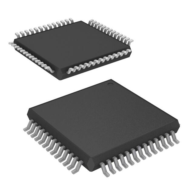
Package Diagram
Figure 6. 52-Pin Thin Plastic Quad Flat Pack (10 × 10 × 1.4 mm) A52 and AZ52
51-85131 *A
Document Number: 38-07336 Rev. *J
Page 12 of 15
[+] Feedback
�PRELIMINARY
RoboClock® CY7B9945V
Acronyms
Table 6. Acronyms Used in this Documnent Acronym FSM LVPECL LVTTL OE RMS PLL TQFP VCO Description Finite State Machine Low-voltage positive emitter coupled logic Low-voltage transistor transistor logic Output enable Root mean square Phase locked loop Thin quad flat pack Voltage controlled oscillator
Document Conventions
Units of Measure
Table 7. Units of Measure Symbol °C dB dBc/Hz fC fF Hz KB Kbit kHz kΩ MHz MΩ µA µF µH µs µV Unit of Measure degrees Celsius decibels decibels relative to the carrier per Hertz femtoCoulomb femtofarads hertz 1024 bytes 1024 bits kilohertz kilohms megahertz megaohms microamperes microfarads microhenrys microseconds microvolts Symbol µVrms µW mA mm ms mV nA ns nV Ω pA pF pp ppm ps sps σ Unit of Measure microvolts root-mean-square microwatts milliamperes millimeters milliseconds millivolts nanoamperes nanoseconds nanovolts ohms picoamperes picofarads peak-to-peak parts per million picoseconds samples per second sigma: one standard deviation
Document Number: 38-07336 Rev. *J
Page 13 of 15
[+] Feedback
�PRELIMINARY
RoboClock® CY7B9945V
Document History Page
Document Title: CY7B9945V RoboClock® High Speed Multi-phase PLL Clock Buffer Document Number: 38-07336 Revision ** *A *B ECN 111747 116572 119078 Orig. of Change CTK HWT HWT Submission Date 03/04/02 09/05/02 10/16/02 New Data Sheet Added TTB Features Corrected the following items in the Electrical Characteristics table: IIIL,IIIH,IIIM specifications from: three level input pins excluding FBFO to FS[0:2],IF[0:3],FBDS[0:1] and FBFO to 2F[0:1],[1:2]DS[0:1],FBFO Common Mode Range (VCOM) from VCC to VCC–0.2 Corrected typo TQFP to LQFP in Features Corrected typo LQFP to TQFP in Features Added clock input frequency (fin) specifications in the switching characteristics table. Minor Change: Fixed the Typical Outputs (Fig. 1) diagram Updated Ordering Information table, primarily to add Pb-free devices Changed instances of “50W” to “50Ω” on page 1. Changed “Pb” to “lead” in Ordering Information package type section. Added “Not recommended for new designs” note to all Pb packages. Added Table of Contents Updated Ordering Information table Updated Package Diagram Updated Sales, Solutions, and Legal Information Removed inactive part from Ordering Information table. Template updates. Included ordering code definitions, acronyms, and units of measure. Description of Change
*C *D *E *F *G
124645 128464 272075 1187144 2761988
RGL RGL RGL KVM CXQ
03/20/03 07/25/03 See ECN See ECN 09/10/09
*H
2891379
KVM
03/12/2010
*I *J
2905846 3196237
KVM BASH
04/06/2010 03/15/11
Document Number: 38-07336 Rev. *J
Page 14 of 15
[+] Feedback
�PRELIMINARY
RoboClock® CY7B9945V
Sales, Solutions, and Legal Information
Worldwide Sales and Design Support
Cypress maintains a worldwide network of offices, solution centers, manufacturer’s representatives, and distributors. To find the office closest to you, visit us at Cypress Locations.
Products
Automotive Clocks & Buffers Interface Lighting & Power Control Memory Optical & Image Sensing PSoC Touch Sensing USB Controllers Wireless/RF cypress.com/go/automotive cypress.com/go/clocks cypress.com/go/interface cypress.com/go/powerpsoc cypress.com/go/plc cypress.com/go/memory cypress.com/go/image cypress.com/go/psoc cypress.com/go/touch cypress.com/go/USB cypress.com/go/wireless
PSoC Solutions
psoc.cypress.com/solutions PSoC 1 | PSoC 3 | PSoC 5
© Cypress Semiconductor Corporation, 2002-2011. The information contained herein is subject to change without notice. Cypress Semiconductor Corporation assumes no responsibility for the use of any circuitry other than circuitry embodied in a Cypress product. Nor does it convey or imply any license under patent or other rights. Cypress products are not warranted nor intended to be used for medical, life support, life saving, critical control or safety applications, unless pursuant to an express written agreement with Cypress. Furthermore, Cypress does not authorize its products for use as critical components in life-support systems where a malfunction or failure may reasonably be expected to result in significant injury to the user. The inclusion of Cypress products in life-support systems application implies that the manufacturer assumes all risk of such use and in doing so indemnifies Cypress against all charges. Any Source Code (software and/or firmware) is owned by Cypress Semiconductor Corporation (Cypress) and is protected by and subject to worldwide patent protection (United States and foreign), United States copyright laws and international treaty provisions. Cypress hereby grants to licensee a personal, non-exclusive, non-transferable license to copy, use, modify, create derivative works of, and compile the Cypress Source Code and derivative works for the sole purpose of creating custom software and or firmware in support of licensee product to be used only in conjunction with a Cypress integrated circuit as specified in the applicable agreement. Any reproduction, modification, translation, compilation, or representation of this Source Code except as specified above is prohibited without the express written permission of Cypress. Disclaimer: CYPRESS MAKES NO WARRANTY OF ANY KIND, EXPRESS OR IMPLIED, WITH REGARD TO THIS MATERIAL, INCLUDING, BUT NOT LIMITED TO, THE IMPLIED WARRANTIES OF MERCHANTABILITY AND FITNESS FOR A PARTICULAR PURPOSE. Cypress reserves the right to make changes without further notice to the materials described herein. Cypress does not assume any liability arising out of the application or use of any product or circuit described herein. Cypress does not authorize its products for use as critical components in life-support systems where a malfunction or failure may reasonably be expected to result in significant injury to the user. The inclusion of Cypress’ product in a life-support systems application implies that the manufacturer assumes all risk of such use and in doing so indemnifies Cypress against all charges. Use may be limited by and subject to the applicable Cypress software license agreement.
Document Number: 38-07336 Rev. *J
Revised March 15, 2011
Page 15 of 15
PSoC Designer™, Programmable System-on-Chip™, and PSoC Express™ are trademarks and PSoC® is a registered trademark of Cypress Semiconductor Corp. All other trademarks or registered trademarks referenced herein are property of the respective corporations.Purchase of I2C components from Cypress or one of its sublicensed Associated Companies conveys a license under the Philips I2C Patent Rights to use these components in an I2C system, provided that the system conforms to the I2C Standard Specification as defined by Philips.All products and company names mentioned in this document may be the trademarks of their respective holders. RoboClock is a registered trademark, and Total Timing Budget and TTB are trademarks of Cypress Semiconductor.
[+] Feedback
�


 工商网监
湘ICP备2023018690号
工商网监
湘ICP备2023018690号
