CY7B9945V RoboClock®
High-Speed Multi-Phase
PLL Clock Buffer
High-Speed Multi-Phase PLL Clock Buffer
Features
Functional Description
■
500 ps max Total Timing Budget (TTB™) window
The CY7B9945V high-speed multi-phase PLL clock buffer offers
user selectable control over system clock functions. This multiple
output clock driver provides the system integrator with functions
necessary to optimize the timing of high performance computer
and communication systems.
■
24 MHz–200 MHz input and Output Operation
■
Low Output-output skew < 200 ps
■
10 + 1 LVTTL outputs driving 50 terminated lines
■
Dedicated feedback output
■
Phase adjustments in 625 ps/1300 ps steps up to +10.4 ns
■
3.3-V LVTTL/LVPECL, Fault Tolerant, and Hot Insertable
Reference Inputs
■
Multiply or Divide Ratios of 1 through 6, 8, 10, and 12
■
Individual Output Bank Disable
■
Output High Impedance Option for Testing Purposes
■
Integrated Phase Locked Loop (PLL) with Lock Indicator
■
Low Cycle-cycle jitter ( 1100 V
Latch-up Current ................................................. > ± 200 mA
Operating Range
Range
Ambient Temperature
VCC
Commercial
0 °C to +70 °C
3.3 V 10%
Industrial
–40 °C to +85 °C
3.3 V 10%
Electrical Characteristics
Over the Operating Range
Description
LVTTL HIGH Voltage
LVTTL LOW Voltage
Test Conditions
Min
Max
Unit
(QF, 1Q[0:3], 2Q[0:5])
VCC = Min, IOH = –30 mA
2.4
–
V
LOCK
IOH = –2 mA, VCC = Min
2.4
–
V
(QF, 1Q[0:3], 2Q[0:5])
VCC = Min, IOL= 30 mA
–
0.5
V
LOCK
IOL= 2 mA, VCC = Min
–
0.5
V
–100
100
A
VCC + 0.3
V
High impedance State Leakage Current
LVTTL Input HIGH
Min < VCC < Max
2.0
LVTTL Input LOW
Min. < VCC < Max.
–0.3
0.8
V
LVTTL VIN >VCC
VCC = GND, VIN = 3.63 V
–
100
A
LVTTL Input HIGH Current
VCC = Max, VIN = VCC
–
500
A
LVTTL Input LOW Current
VCC = Max, VIN = GND
–500
–
A
Min < VCC < Max
0.87 × VCC
–
V
Min < VCC < Max
0.47 × VCC 0.53 × VCC
Three level Input HIGH
[4]
Three level Input MID[4]
[4]
Three level Input LOW
Three level Input HIGH Current
FS[0:2],IF[0:3],FBDS[0:1]
Three level Input MID Current
FS[0:2],IF[0:3],FBDS[0:1]
Min < VCC < Max
–
0.13 × VCC
V
VIN = VCC
–
200
A
2F[0:1],[1:2]DS[0:1],FBFO
VIN = VCC/2
2F[0:1],[1:2]DS[0:1],FBFO
Three level Input LOW Current
FS[0:2],IF[0:3],FBDS[0:1]
V
VIN = GND
–
400
A
–50
50
A
–100
100
A
–200
–
A
–400
–
A
Input Differential Voltage
400
VCC
mV
Highest Input HIGH Voltage
1.0
VCC
V
Lowest Input LOW Voltage
GND
VCC – 0.4
V
2F[0:1],[1:2]DS[0:1],FBFO
0.8
VCC – 0.2
V
Internal Operating Current
CY7B9945V
VCC = Max, fMAX[5]
–
250
mA
Output Current
Dissipation/Pair[4]
CY7B9945V
VCC = Max, CLOAD = 25 pF,
RLOAD = 50 at VCC/2, fMAX
–
40
mA
Common Mode Range (Crossing Voltage)
Notes
4. These inputs are normally wired to VCC, GND, or left unconnected (actual threshold voltages vary as a percentage of VCC). Internal termination resistors hold the
unconnected inputs at VCC/2. If these inputs are switched, the function and timing of the outputs may glitch and the PLL may require an additional tLOCK time before
all data sheet limits are achieved.
5. This is for non-three level inputs.
Document Number: 38-07336 Rev. *P
Page 9 of 19
�CY7B9945V RoboClock®
Capacitance
Parameter
CIN
Description
Test Conditions
Input capacitance
Min
Max
Unit
–
5
pF
Test Conditions
52-pin TQFP
Unit
Test conditions follow standard test methods and
procedures for measuring thermal impedance, in
accordance with EIA/JESD51.
55
°C/W
16
°C/W
TA = 25 °C, f = 1 MHz, VCC = 3.3 V
Thermal Resistance
Parameter [6]
Description
θJA
Thermal resistance
(junction to ambient)
θJC
Thermal resistance
(junction to case)
AC Test Loads and Waveforms
Figure 4. AC Test Loads and Waveforms [7]
For LOCK output only
R1 = 910
R2 = 910
CL < 30 pF
For all other outputs
R1 = 100
R2 = 100
CL < 25 pF to 185 MHz
or 10 pF at 200 MHz
(Includes fixture and
probe capacitance)
3.3 V
R1
OUTPUT
CL
R2
(a) LVTTL AC Test Load
3.3 V
2.0 V
0.8 V
GND
2.0 V
0.8 V
< 1 ns
< 1 ns
(b) TTL Input Test Waveform
Notes
6. These parameters are guaranteed by design and are not tested.
7. Assumes 25 pF Maximum Load Capacitance up to 185 MHz. At 200 MHz the maximum load is 10 pF.
Document Number: 38-07336 Rev. *P
Page 10 of 19
�CY7B9945V RoboClock®
Switching Characteristics
Over the Operating Range [8, 9, 10, 11, 12]
Parameter
CY7B9945V-2
Description
Min
Max
Unit
fin
Clock Input Frequency
24
200
MHz
fout
Clock Output Frequency
24
200
MHz
–
200
ps
tSKEWPR
tSKEWBNK
Matched Pair Skew
Intrabank Skew
[13, 14]
, 1Q[0:1], 1Q[2:3], 2Q[0:1], 2Q[2:3], 2Q[4:5]
[13, 14]
–
250
ps
tSKEW0
Output-Output Skew (same frequency and phase, rise to rise, fall to fall)
[13, 14]
–
250
ps
tSKEW1
Output-Output Skew (same frequency and phase, other banks at different
frequency,
rise to rise, fall to fall) [13, 14]
–
250
ps
tSKEW2
Output-Output Skew
(all output configurations outside of tSKEW0 and tSKEW1) [12, 15]
–
500
ps
tCCJ1-3
Cycle-to-Cycle Jitter (divide by 1 output frequency,
FB = divide by 1, 2, 3)
–
150
ps
PeakPeak
tCCJ4-12
Cycle-to-Cycle Jitter (divide by 1 output frequency,
FB = divide by 4, 5, 6, 8, 10, 12)
–
100
ps
PeakPeak
tPD
Propagation Delay, REF to FB Rise
–250
250
ps
TTB
Total Timing Budget window
(same frequency and phase) [16, 17]
–
500
ps
tPDDELTA
Propagation Delay difference between two devices [18]
–
200
ps
tREFpwh
REF input (Pulse Width
HIGH)[8]
2.0
–
ns
tREFpwl
REF input (Pulse Width LOW)[8]
2.0
–
ns
0.15
2.0
ns
10
ms
Time[21]
tr/tf
Output Rise/Fall
tLOCK
PLL Lock TIme From Power Up
–
tRELOCK1
PLL Relock Time (from same frequency, different phase) with Stable Power Supply
–
500
s
tRELOCK2
PLL Re-lock Time (from different frequency, different phase) with Stable Power
Supply[20]
–
1000
s
Notes
8. This is for non-three level inputs.
9. Both outputs of pair must be terminated, even if only one is being used.
10. Each package must be properly decoupled.
11. AC parameters are measured at 1.5 V, unless otherwise indicated.
12. Test Load CL= 25 pF, terminated to VCC/2 with 50up to185 MHz and 10 pF load to 200 MHz.
13. Tested initially and after any design or process changes that affect these parameters.
14. TTB is the window between the earliest and the latest output clocks with respect to the input reference clock across variations in output frequency, supply voltage,
operating temperature, input clock edge rate, and process. The measurements are taken with the AC test load specified and include output-output skew, cycle-cycle
jitter, and dynamic phase error. TTB is equal to or smaller than the maximum specified value at a given output frequency.
15. SKEW is defined as the time between the earliest and the latest output transition among all outputs for which the same phase delay has been selected when all
outputs are loaded with 25 pF and properly terminated up to 185 MHz. At 200 MHz the max load is 10 pF.
16. Guaranteed by statistical correlation. Tested initially and after any design or process changes that affects these parameters.
17. Rise and fall times are measured between 2.0 V and 0.8 V.
18. fNOM must be within the frequency range defined by the same FS state.
19. tPWH is measured at 2.0 V. tPWL is measured at 0.8 V.
20. fNOM must be within the frequency range defined by the same FS state.
Document Number: 38-07336 Rev. *P
Page 11 of 19
�CY7B9945V RoboClock®
Switching Characteristics (continued)
Over the Operating Range [8, 9, 10, 11, 12]
Parameter
tODCV
tPWH
tPWL
CY7B9945V-2
Description
Output duty cycle deviation from 50%[21]
Output HIGH time deviation from 50%
Output LOW time deviation from 50%
[22]
[22]
[23]
Unit
Min
Max
–1.0
1.0
ns
–
1.5
ns
–
2.0
ns
tPDEV
Period deviation when changing from reference to reference
–
0.025
UI
tOAZ
DIS[1:2] HIGH to output high-impedance from ACTIVE [24, 25]
1.0
10
ns
tOZA
DIS[1:2] LOW to output ACTIVE from output is high impedance [25]
0.5
14
ns
Notes
21. SKEW is defined as the time between the earliest and the latest output transition among all outputs for which the same phase delay has been selected when all
outputs are loaded with 25 pF and properly terminated up to 185 MHz. At 200 MHz the max load is 10 pF.
22. Measured at 0.5 V deviation from starting voltage.
23. For tOZA minimum, CL = 0 pF. For tOZA maximum, CL= 25 pF to 185 MHz or 10 pF to 200 MHz.
24. Tested initially and after any design or process changes that affect these parameters.
25. These figures are for illustration purposes only. The actual ATE loads may vary.
Document Number: 38-07336 Rev. *P
Page 12 of 19
�CY7B9945V RoboClock®
AC Timing Diagram
Figure 5. AC Timing Diagram
tREFpwl
tREFpwh
[1:2]Q[0,2]
REF
t SKEWPR
t SKEWPR
t PWH
tPD
t PWL
[1:2]Q[1,3]
2.0 V
FB
0.8 V
tCCJ1-3,4-12
Q
[1:2]Q[0:3]
t SKEWBNK
t SKEWBNK
[1:2]Q[0:3]
REF TO DEVICE 1 and 2
tODCV
tPD
tODCV
Q
FB DEVICE1
tPDELTA
tPDELTA
t SKEW0,1
t SKEW0,1
Other Q
FB DEVICE2
Document Number: 38-07336 Rev. *P
Page 13 of 19
�CY7B9945V RoboClock®
Ordering Information
Propagation
Delay (ps)
Max. Speed
(MHz)
Package
Name
Ordering Code
Operating
Range
Package Type
Pb-free
250
200
CY7B9945V-2AXI
AZ52
52-pin TQFP
Industrial
200
CY7B9945V-2AXIT
AZ52
52-pin TQFP – Tape and Reel
Industrial
Ordering Code Definitions
CY
XXXXXX
V
-
2
A
X
C
T
T = Tape and reel, Blank = Tube
Temperature range: C = Commercial
Pb-free, Blank = leaded
52-pin TQFP package
Speed grade
Operating voltage: 3.3 V
Part identifier
Company Code: CY = Cypress
Document Number: 38-07336 Rev. *P
Page 14 of 19
�CY7B9945V RoboClock®
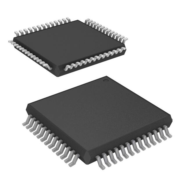
Package Diagram
Figure 6. 52-pin TQFP (10 × 10 × 1.4 mm) Package Outline, 51-85131
51-85131 *C
Document Number: 38-07336 Rev. *P
Page 15 of 19
�CY7B9945V RoboClock®
Acronyms
Table 6. Acronyms Used in this Document
Acronym
Description
FSM
Finite State Machine
LVPECL
Low-Voltage Positive Emitter Coupled Logic
LVTTL
Low-Voltage Transistor-Transistor Logic
OE
Output Enable
RMS
Root Mean Square
PLL
Phase Locked Loop
TQFP
Thin Quad Flat Pack
VCO
Voltage Controlled Oscillator
Document Conventions
Units of Measure
Table 7. Units of Measure
Symbol
Unit of Measure
Symbol
µVrms
Unit of Measure
°C
degrees Celsius
microvolts root-mean-square
dB
decibel
µW
microwatt
dBc/Hz
decibels relative to the carrier per Hertz
mA
milliampere
fC
femtoCoulomb
mm
millimeter
fF
femtofarad
ms
millisecond
Hz
hertz
mV
millivolt
KB
1024 bytes
nA
nanoampere
Kbit
1024 bits
ns
nanosecond
kHz
kilohertz
nV
nanovolt
k
kilohm
ohm
MHz
megahertz
pA
picoampere
M
megaohm
pF
picofarad
µA
microampere
pp
peak-to-peak
µF
microfarad
ppm
parts per million
µH
microhenry
ps
picosecond
µs
microsecond
sps
samples per second
µV
microvolt
sigma: one standard deviation
Document Number: 38-07336 Rev. *P
Page 16 of 19
�CY7B9945V RoboClock®
Document History Page
Document Title: CY7B9945V RoboClock®, High-Speed Multi-Phase PLL Clock Buffer
Document Number: 38-07336
Revision
ECN
Orig. of
Change
Submission
Date
**
111747
CTK
03/04/2002
New data sheet.
*A
116572
HWT
09/05/2002
Updated Features:
Added “500 ps max. Total Timing Budget™ (TTB™) window”.
*B
119078
HWT
10/16/2002
Updated Features:
Removed “52-pin TQFP package”.
Added “52-pin 1.4-mm LQFF package”.
Updated Electrical Characteristics:
Replaced “Three-level Input Pins (FS[0:2], 1F[0:3], 2F[0:1], [1:2]DS[0:1],
FBFO, FBDS[0:1])” with “Three-level Input Pins (FS[0:2], 1F[0:3], 2F[0:1],
[1:2]DS[0:1], FBFO, FBDS[0:1], MODE)” in sub section heading.
Updated details in “Test Conditions” and “Min.” columns corresponding to IIHH,
IIMM, IILL parameters.
Changed maximum value of VCOM parameter from “VCC” to “VCC – 0.2 V”.
*C
124645
RGL
03/20/2003
Updated Features:
Removed “52-pin 1.4-mm LQFF package”.
Added “52-pin 1.4-mm TQFP package”.
*D
128464
RGL
07/25/2003
Updated Switching Characteristics:
Added fin parameter and its corresponding details.
*E
272075
RGL
10/01/2004
Minor Change: Fixed typo in Figure 2.
*F
1187144
KVM
06/25/2007
Changed status from Final to Preliminary.
Updated Ordering Information:
Updated part numbers.
Added Note “Not recommended for new designs.” and referred the same note
in CY7B9945V-5AI.
Updated to new template.
*G
2761988
CXQ
09/10/2009
Fixed typo (Replaced “50W” with “50” in all instances across the document).
Updated Ordering Information:
No change in part numbers.
Replaced “Pb” with “pin” in “Package Type” column.
Referred Note “Not recommended for new designs” in all MPNs with Pb
packages.
*H
2891379
KVM
03/12/2010
Updated Ordering Information:
Updated part numbers.
Updated Package Diagram:
spec 51-85131 – Changed revision from ** to *A.
Updated to new template.
*I
2905846
KVM
04/06/2010
Updated Ordering Information:
Updated part numbers.
*J
3196237
BASH
03/15/2011
Updated Ordering Information:
No change in part numbers.
Added Ordering Code Definitions.
Added Acronyms and Units of Measure.
Updated to new template.
Completing Sunset Review.
*K
4323331
CINM
03/27/2014
Updated Package Diagram:
spec 51-85131 – Changed revision from *A to *C.
Updated to new template.
Completing Sunset Review.
*L
4570146
CINM
11/14/2014
Updated Functional Description:
Added “For a complete list of related documentation, click here.” at the end.
Document Number: 38-07336 Rev. *P
Description of Change
Page 17 of 19
�CY7B9945V RoboClock®
Document History Page (continued)
Document Title: CY7B9945V RoboClock®, High-Speed Multi-Phase PLL Clock Buffer
Document Number: 38-07336
Revision
ECN
Orig. of
Change
Submission
Date
*M
5257087
PSR
05/03/2016
Changed status from Preliminary to Final.
Added Thermal Resistance.
Updated to new template.
*N
5687997
XHT
04/07/2017
Updated to new template.
Completing Sunset Review.
*O
5773768
PSR
06/19/2017
Updated Switching Characteristics:
Removed “CY7B9945V-5” column.
*P
6536055
XHT
04/08/2019
Updated Ordering Information:
Updated part numbers.
Updated to new template.
Document Number: 38-07336 Rev. *P
Description of Change
Page 18 of 19
�CY7B9945V RoboClock®
Sales, Solutions, and Legal Information
Worldwide Sales and Design Support
Cypress maintains a worldwide network of offices, solution centers, manufacturer’s representatives, and distributors. To find the office
closest to you, visit us at Cypress Locations.
PSoC® Solutions
Products
Arm® Cortex® Microcontrollers
Automotive
cypress.com/arm
cypress.com/automotive
Clocks & Buffers
Interface
Internet of Things
Memory
cypress.com/clocks
cypress.com/interface
cypress.com/iot
cypress.com/memory
Microcontrollers
cypress.com/mcu
PSoC
cypress.com/psoc
Power Management ICs
Touch Sensing
USB Controllers
Wireless Connectivity
PSoC 1 | PSoC 3 | PSoC 4 | PSoC 5LP | PSoC 6 MCU
Cypress Developer Community
Community | Projects | Video | Blogs | Training | Components
Technical Support
cypress.com/support
cypress.com/pmic
cypress.com/touch
cypress.com/usb
cypress.com/wireless
© Cypress Semiconductor Corporation, 2002–2019. This document is the property of Cypress Semiconductor Corporation and its subsidiaries (“Cypress”). This document, including any software or
firmware included or referenced in this document (“Software”), is owned by Cypress under the intellectual property laws and treaties of the United States and other countries worldwide. Cypress
reserves all rights under such laws and treaties and does not, except as specifically stated in this paragraph, grant any license under its patents, copyrights, trademarks, or other intellectual property
rights. If the Software is not accompanied by a license agreement and you do not otherwise have a written agreement with Cypress governing the use of the Software, then Cypress hereby grants
you a personal, non-exclusive, nontransferable license (without the right to sublicense) (1) under its copyright rights in the Software (a) for Software provided in source code form, to modify and reproduce
the Software solely for use with Cypress hardware products, only internally within your organization, and (b) to distribute the Software in binary code form externally to end users (either directly or
indirectly through resellers and distributors), solely for use on Cypress hardware product units, and (2) under those claims of Cypress’s patents that are infringed by the Software (as provided by
Cypress, unmodified) to make, use, distribute, and import the Software solely for use with Cypress hardware products. Any other use, reproduction, modification, translation, or compilation of the
Software is prohibited.
TO THE EXTENT PERMITTED BY APPLICABLE LAW, CYPRESS MAKES NO WARRANTY OF ANY KIND, EXPRESS OR IMPLIED, WITH REGARD TO THIS DOCUMENT OR ANY SOFTWARE
OR ACCOMPANYING HARDWARE, INCLUDING, BUT NOT LIMITED TO, THE IMPLIED WARRANTIES OF MERCHANTABILITY AND FITNESS FOR A PARTICULAR PURPOSE. No computing
device can be absolutely secure. Therefore, despite security measures implemented in Cypress hardware or software products, Cypress shall have no liability arising out of any security breach, such
as unauthorized access to or use of a Cypress product. CYPRESS DOES NOT REPRESENT, WARRANT, OR GUARANTEE THAT CYPRESS PRODUCTS, OR SYSTEMS CREATED USING
CYPRESS PRODUCTS, WILL BE FREE FROM CORRUPTION, ATTACK, VIRUSES, INTERFERENCE, HACKING, DATA LOSS OR THEFT, OR OTHER SECURITY INTRUSION (collectively, “Security
Breach”). Cypress disclaims any liability relating to any Security Breach, and you shall and hereby do release Cypress from any claim, damage, or other liability arising from any Security Breach. In
addition, the products described in these materials may contain design defects or errors known as errata which may cause the product to deviate from published specifications. To the extent permitted
by applicable law, Cypress reserves the right to make changes to this document without further notice. Cypress does not assume any liability arising out of the application or use of any product or
circuit described in this document. Any information provided in this document, including any sample design information or programming code, is provided only for reference purposes. It is the
responsibility of the user of this document to properly design, program, and test the functionality and safety of any application made of this information and any resulting product. “High-Risk Device”
means any device or system whose failure could cause personal injury, death, or property damage. Examples of High-Risk Devices are weapons, nuclear installations, surgical implants, and other
medical devices. “Critical Component” means any component of a High-Risk Device whose failure to perform can be reasonably expected to cause, directly or indirectly, the failure of the High-Risk
Device, or to affect its safety or effectiveness. Cypress is not liable, in whole or in part, and you shall and hereby do release Cypress from any claim, damage, or other liability arising from any use of
a Cypress product as a Critical Component in a High-Risk Device. You shall indemnify and hold Cypress, its directors, officers, employees, agents, affiliates, distributors, and assigns harmless from
and against all claims, costs, damages, and expenses, arising out of any claim, including claims for product liability, personal injury or death, or property damage arising from any use of a Cypress
product as a Critical Component in a High-Risk Device. Cypress products are not intended or authorized for use as a Critical Component in any High-Risk Device except to the limited extent that (i)
Cypress’s published data sheet for the product explicitly states Cypress has qualified the product for use in a specific High-Risk Device, or (ii) Cypress has given you advance written authorization to
use the product as a Critical Component in the specific High-Risk Device and you have signed a separate indemnification agreement.
Cypress, the Cypress logo, Spansion, the Spansion logo, and combinations thereof, WICED, PSoC, CapSense, EZ-USB, F-RAM, and Traveo are trademarks or registered trademarks of Cypress in
the United States and other countries. For a more complete list of Cypress trademarks, visit cypress.com. Other names and brands may be claimed as property of their respective owners.
Document Number: 38-07336 Rev. *P
Revised April 8, 2019
RoboClock is a registered trademark, and Total Timing Budget and TTB are trademarks of Cypress Semiconductor Corporation.
Page 19 of 19
�


 工商网监
湘ICP备2023018690号
工商网监
湘ICP备2023018690号
