CY7C43642 CY7C43662 CY7C43682
1K/4K/16K x36 x2 Bidirectional Synchronous FIFO
Features
• High-speed, low-power, bidirectional, First-In, First-Out (FIFO) memories • 1Kx36x2 (CY7C43642) • 4Kx36x2 (CY7C43662) • 16Kx36x2 (CY7C43682) • 0.35-micron CMOS for optimum speed/power • High speed 133-MHz operation (7.5-ns read/write cycle times) • Low power — ICC= 100 mA — ISB= 10 mA • Fully asynchronous and simultaneous read and write operation permitted • Mailbox bypass register for each FIFO • Parallel Programmable Almost Full and Almost Empty flags • Retransmit function • Standard or FWFT mode user selectable • 120-pin TQFP packaging • Easily expandable in width and depth
Logic Block Diagram
MBF1 CLKA CSA W/RA ENA MBA RT2
Port A Control Logic Input Register
Mail1 Register
CLKB CSB W/RB ENB MBB RT1
Register
RST1
FIFO1, Mail1 Reset Logic
Write Pointer
Read Pointer
FFA/IRA AFA
Status Flag Logic
Output
1K/4K/16K x36 Dual Ported Memory
Port B Control Logic
EFB/ORB AEB
FS0 FS1 A0–35 EFA/ORA AEA
Programmable Flag Offset Registers
Timing Mode
B0–35 FWFT/STAN
Status Flag Logic Write Pointer Read Pointer
FFB/IRB AFB
Output Register
256/512/1K 4K/16K x36 Dual Ported Memory
Mail2 Register
MBF2
Cypress Semiconductor Corporation Document #: 38-06019 Rev. *B
•
3901 North First Street
•
San Jose
Input Register
FIFO2, Mail2 Reset Logic
RST2
•
CA 95134 • 408-943-2600 Revised December 26, 2002
�CY7C43642 CY7C43662 CY7C43682
Pin Configuration
TQFP Top View
RST2 MBB MBF1 VCC
A35 A34 A33 A32 VCC A31 A30 GND A29 A28 A27 A26 A25 A24 A23 FWFT/STAN A22 VCC A21 A20 A19 A18 GND A17 A16 A15 A14 A13 RT2 A12
120 119 118 117 116 115 114 113 112 111 110 109 108 107 106 105 104 103 102 101 100 99 98 97 96 95 94 93 92 91
GND CLKA ENA W/RA CSA FFA/IRA EFA/ORA VCC AFA AEA MBF2 MBA RST1 FS0 GND FS1
AEB AFB EFB/ORB FFB/IRB GND CSB W/RB ENB CLKB VCC 90 89 88 87 86 85 84 83 82 81 80 79 78 77 76 75 74 73 72 71 70 69 68 67 66 65 64 63 62 61
1 2 3 4 5 6 7 8 9 10 11 12 13 14 15 16 17 18 19 20 21 22 23 24 25 26 27 28 29 30
CY7C43642 CY7C43662 CY7C43682
B35 B34 B33 B32 GND B31 B30 B29 B28 B27 B26 RT1 B25 B24 GND B23 B22 B21 B20 B19 B18 GND B17 B16 VCC B15 B14 B13 B12 GND
GND A11 A10 A9
Document #: 38-06019 Rev. *B
B4 B5 GND B6 VCC B7 B8 B9 B10 B11
A8 A7 A6 GND A5 A4 A3 VCC A2 A1 A0 GND
B0 B1 B2 B3
31 32 33 34 35 36 37 38 39 40 41 42 43 44 45 46 47 48 49 50 51 52 53 54 55 56 57 58 59 60
Page 2 of 30
�CY7C43642 CY7C43662 CY7C43682
Functional Description
The CY7C436X2 is a monolithic, high-speed, low-power, CMOS Bidirectional Synchronous (clocked) FIFO memory which supports clock frequencies up to 133 MHz and has read access times as fast as 6 ns. Two independent 1K/4K/16K x 36 dual-port SRAM FIFOs on board each chip buffer data in opposite directions. The CY7C436X2 is a synchronous (clocked) FIFO, meaning each port employs a synchronous interface. All data transfers through a port are gated to the LOW-to-HIGH transition of a port clock by enable signals. The clocks for each port are independent of one another and can be asynchronous or coincident. The enables for each port are arranged to provide a simple bidirectional interface between microprocessors and/or buses with synchronous control. Communication between each port may bypass the FIFOs via two mailbox registers. The mailbox registers’ width matches the selected Port B bus width. Each mailbox register has a flag (MBF1 and MBF2) to signal when new mail has been stored. Master Reset initializes the read and write pointers to the first location of the memory array, and selects parallel flag programming, or one of the three possible default flag offset settings, 8, 16, or 64. Each FIFO has its own independent Master Reset pin, RST1 and RST2. The CY7C436X2 have two modes of operation: In the CY Standard Mode, the first word written to an empty FIFO is deposited into the memory array. A read operation is required to access that word (along with all other words residing in memory). In the First-Word Fall-Through Mode (FWFT), the first word (36-bit wide) written to an empty FIFO appears automatically on the outputs, no read operation required (nevertheless, accessing subsequent words does necessitate a formal read request). The state of the FWFT/STAN pin during FIFO operation determines the mode in use. Each FIFO has a combined Empty/Output Ready Flag (EFA/ORA and EFB/ORB) and a combined Full/Input Ready Flag (FFA/IRA and FFB/IRB). The EF and FF functions are selected in the CY Standard Mode. EF indicates whether the memory is full or not. The IR and OR functions are selected in the First-Word Fall-Through Mode. IR indicates whether or not the FIFO has available memory locations. OR shows whether the FIFO has data available for reading or not. It marks the presence of valid data on the outputs.[1] Each FIFO has a programmable Almost Empty flag (AEA and AEB) and a programmable Almost Full flag (AFA and AFB). AEA and AEB indicate when a selected number of words written to FIFO memory achieve a predetermined “almost empty state.” AFA and AFB indicate when a selected number of words written to the memory achieve a predetermined “almost full state.”[2] IRA, IRB, AFA, and AFB are synchronized to the port clock that writes data into its array. ORA, ORB, AEA, and AEB are synchronized to the port clock that reads data from its array. Programmable offset for AEA, AEB, AFA, and AFB are loaded in parallel using Port A. Three default offset settings are also provided. The AEA and AEB threshold can be set at 8, 16, or 64 locations from the empty boundary and AFA and AFB threshold can be set at 8, 16, or 64 locations from the full boundary. All these choices are made using the FS0 and FS1 inputs during Master Reset. Two or more devices may be used in parallel to create wider data paths. The CY7C436X2 are characterized for operation from 0°C to 70°C commercial, and from –40°C to 85°C industrial. Input ESD protection is greater than 2001V, and latch-up is prevented by the use of guard rings.
Selection Guide
CY7C43642/62/82 -7 Maximum Frequency (MHz) Maximum Access Time (ns) Minimum Cycle Time (ns) Minimum Data or Enable Set-up (ns) Minimum Data or Enable Hold (ns) Maximum Flag Delay (ns) Active Power Supply Current (ICC1) (mA) Commercial Industrial CY7C43642 Density Package 1K x 36 120 TQFP CY7C43662 4K x 36 120 TQFP 133 6 7.5 3 0 6 100 CY7C43642/62/82 -10 100 8 10 4 0 8 100 CY7C43642/62/82 -15 66.7 10 15 5 0 8 100 100 CY7C43682 16K x 36 120 TQFP
Notes: 1. When reading from the FIFO under FWFT, ORA/ORB signal should be included in the read logic to ensure proper operation. To read without gating the boundary flag (e.g., in bursts), use CY standard mode. 2. When FIFO is operated at the almost empty/full boundary, there may be an uncertainty of up to 3 clock cycles for flag assertion and deassertion. Refer to “Designing with CY7C436xx Synchronous FIFO” application notes for more details on flag uncertainties.
Document #: 38-06019 Rev. *B
Page 3 of 30
�CY7C43642 CY7C43662 CY7C43682
Pin Definitions
Signal Name A0–35 AEA Description Port A Data Port A Almost Empty Flag Port B Almost Empty Flag Port A Almost Full Flag Port B Almost Full Flag Port B Data I/O O Function Programmable Almost Empty flag synchronized to CLKA. It is LOW when the number of words in FIFO2 is less than or equal to the value in the Almost Empty A offset register, X2.[2] Programmable Almost Empty flag synchronized to CLKB. It is LOW when the number of words in FIFO1 is less than or equal to the value in the Almost Empty B offset register, X1.[2] Programmable Almost Full flag synchronized to CLKA. It is LOW when the number of empty locations in FIFO1 is less than or equal to the value in the Almost Full A offset register, Y1.[2] Programmable Almost Full flag synchronized to CLKB. It is LOW when the number of empty locations in FIFO2 is less than or equal to the value in the Almost Full B offset register, Y2.[2] During Master Reset. A HIGH on FWFT selects CY Standard mode, a LOW selects First-Word Fall-Through mode. Once the timing mode has been selected, the level on FWFT/STAN must be static throughout device operation. CLKA is a continuous clock that synchronizes all data transfers through Port A and can be asynchronous or coincident to CLKB. FFA/IRA, EFA/ORA, AFA, and AEA are all synchronized to the LOW-to-HIGH transition of CLKA. CLKB is a continuous clock that synchronizes all data transfers through Port B and can be asynchronous or coincident to CLKA. FFB/IRB, EFB/ORB, AFB, and AEB are all synchronized to the LOW-to-HIGH transition of CLKB. CSA must be LOW to enable a LOW-to HIGH transition of CLKA to read or write on Port A. The A0–35 outputs are in the high-impedance state when CSA is HIGH. CSB must be LOW to enable a LOW-to HIGH transition of CLKB to read or write on Port B. The B0–35 outputs are in the high-impedance state when CSB is HIGH. This is a dual-function pin. In the CY Standard Mode, the EFA function is selected. EFA indicates whether or not the FIFO2 memory is empty. In the FWFT mode, the ORA function is selected. ORA indicates the presence of valid data on A0–35 outputs, available for reading. EFA/ORA is synchronized to the LOW-to-HIGH transition of CLKA.[1] This is a dual-function pin. In the CY Standard Mode, the EFB function is selected. EFB indicates whether or not the FIFO1 memory is empty. In the FWFT mode, the ORB function is selected. ORB indicates the presence of valid data on B0–35 outputs, available for reading. EFB/ORB is synchronized to the LOW-to-HIGH transition of CLKB.[1] ENA must be HIGH to enable a LOW-to-HIGH transition of CLKA to read or write data on Port A. ENB must be HIGH to enable a LOW-to-HIGH transition of CLKB to read or write data on Port B. This is a dual-function pin. In the CY Standard Mode, the FFA function is selected. FFA indicates whether or not the FIFO1 memory is full. In the FWFT mode, the IRA function is selected. IRA indicates whether or not there is space available for writing to the FIFO1 memory. FFA/IRA is synchronized to the LOW-to-HIGH transition of CLKA. This is a dual-function pin. In the CY Standard Mode, the FFB function is selected. FFB indicates whether or not the FIFO2 memory is full. In the FWFT mode, the IRB function is selected. IRB indicates whether or not there is space available for writing to the FIFO2 memory. FFB/IRB is synchronized to the LOW-to-HIGH transition of CLKB. I/O 36-bit bidirectional data port for side A.
AEB
O
AFA
O
AFB
O
B0–35
I/O 36-bit bidirectional data port for side B. I
FWFT/STAN Big Endian/First-Wor d Fall-Through Select CLKA Port A Clock
I
CLKB
Port B Clock
I
CSA CSB EFA/ORA
Port A Chip Select Port B Chip Select Port A Empty/ Output Ready Flag Port B Empty/ Output Ready Flag Port A Enable Port B Enable Port A Full/Input Ready Flag
I I O
EFB/ORB
O
ENA ENB FFA/IRA
I I O
FFB/IRB
Port B Full/Input Ready Flag
O
Document #: 38-06019 Rev. *B
Page 4 of 30
�CY7C43642 CY7C43662 CY7C43682
Pin Definitions (continued)
Signal Name FS1 FS0 MBA Description Flag Offset Select 1 Flag Offset Select 0 Port A Mailbox Select I/O I I I Function The LOW-to-HIGH transition of a FIFO’s reset input latches the values of FS0 and FS1. If either FS0 or FS1 is HIGH when a reset input goes HIGH, one of the three preset values (8, 16, or 64) is selected as the offset for the FIFO’s Almost Full and Almost Empty flags. If both FIFOs are reset simultaneously and both FS0 and FS1 are LOW when RST1 and RST2 go HIGH, the first four writes to FIFO1 Almost Empty offsets for both FIFOs. A HIGH level on MBA chooses a mailbox register for a Port A read or write operation. When a read operation is performed on Port A, a HIGH level on MBA selects data from the Mail2 register for output and a LOW level selects FIFO2 output register data for output. When a write operation is performed on Port A, a HIGH level on MBA will write the data into Mail1 register while a LOW level will write the data into FIFO1. A HIGH level on MBB chooses a mailbox register for a Port B read or write operation. When a read operation is performed on Port B, a HIGH level on MBB selects data from the Mail1 register for output and a LOW level selects FIFO1 output register data for output. When a write operation is performed on Port B, a HIGH level on MBB will write the data into Mail2 register while a LOW level will write the data into FIFO2. MBF1 is set LOW by a LOW-to-HIGH transition of CLKA that writes data to the Mail1 register. Writes to the Mail1 register are inhibited while MBF1 is LOW. MBF1 is set HIGH by a LOW-to-HIGH transition of CLKB when a Port B read is selected and MBB is HIGH. MBF1 is set HIGH following either a Master or Partial Reset of FIFO1. MBF2 is set LOW by a LOW-to-HIGH transition of CLKB that writes data to the Mail2 register. Writes to the Mail2 register are inhibited while MBF2 is LOW. MBF2 is set HIGH by a LOW-to-HIGH transition of CLKA when a Port A read is selected and MBA is HIGH. MBF2 is set HIGH following either a Master or Partial Reset of FIFO2. A LOW strobe on this pin will retransmit the data on FIFO1. This is achieved by bringing the read pointer back to location zero. The user will still need to perform read operations to retransmit the data. Retransmit function applies to CY standard mode only. A LOW strobe on this pin will retransmit data on FIFO2. This is achieved by bringing the read pointer back to location zero. The user will still need to perform read operations to retransmit the data. Retransmit function applies to CY standard mode only. A HIGH selects a write operation and a LOW selects a read operation on Port A for a LOW-to-HIGH transition of CLKA. The A0–35 outputs are in the HIGH impedance state when W/RA is HIGH. A LOW selects a write operation and a HIGH selects a read operation on Port B for a LOW-to-HIGH transition of CLKB. The B0–35 outputs are in the HIGH impedance state when W/RB is LOW. A LOW on this pin initializes the FIFO1 read and write pointers to the first location of memory and sets the Port B output register to all zeroes. A LOW pulse on RST1 selects the programming method (serial or parallel) and one of three programmable flag default offsets. It also configures Port A for bus size and endian arrangement. Four LOW-to-HIGH transitions of CLKA and four LOW-to-HIGH transitions of CLKB must occur while RST1 is LOW. A LOW on this pin initializes the FIFO2 read and write pointers to the first location of memory and sets the Port B output register to all zeroes. A LOW pulse on RST2 selects the programming method (serial or parallel) and one of three programmable flag default offsets. It also configures Port B for bus size and endian arrangement. Four LOW-to-HIGH transitions of CLKA and four LOW-to-HIGH transitions of CLKB must occur while RST2 is LOW. Master Reset initializes the internal read and write pointers and forces the Full/Input Ready flag (FFA/IRA, FFB/IRB) LOW, the Empty/Output Ready flag (EFA/ORA, EFB/ORB) LOW, the Almost Empty flag (AEA, AEB) LOW, and the Almost Full flag (AFA, AFB) HIGH. A Master Reset also forces the Mailbox flag (MBF1, MBF2) of the parallel mailbox register HIGH. After a Master Reset, the FIFO’s Full/Input Ready flag is set HIGH after two clock cycles to begin normal operation. A Master
MBB
Port B Mailbox Select
I
MBF1
Mail1 Register Flag
O
MBF2
Mail2 Register Flag
O
RT1
Retransmit FIFO1 Retransmit FIFO2 Port A Write/ Read Select Port B Write/ Read Select FIFO1 Master Reset
I
RT2
I
W/RA
I
W/RB
I
RST1
I
RST2
FIFO2 Master Reset
I
Signal Description
Reset (RST1, RST2) Each of the two FIFO memories of the CY7C436X2 undergoes a complete reset by taking its associated Master Reset (RST1, RST2) input LOW for at least four Port A clock (CLKA) and four Port B clock (CLKB) LOW-to-HIGH transitions. The Master Reset inputs can switch asynchronously to the clocks. A Document #: 38-06019 Rev. *B
Page 5 of 30
�CY7C43642 CY7C43662 CY7C43682
Reset must be performed on the FIFO after power-up, before data is written to its memory. A LOW-to-HIGH transition on a FIFO reset (RST1, RST2) input latches the values of the Flag select (FS0, FS1) for choosing the Almost Full and Almost Empty offset programming method (see Almost Empty and Almost Full flag offset programming below). First-Word Fall-Through (FWFT/STAN) After Master Reset, the FWFT select function is active, permitting a choice between two possible timing modes: CY Standard Mode or First-Word Fall-Through (FWFT) Mode. Once the Master Reset (RST1, RST2) input is HIGH, a HIGH on the FWFT/STAN input during the next LOW-to-HIGH transition of CLKA (for FIFO1) and CLKB (for FIFO2) will select CY Standard Mode. This mode uses the Empty Flag function (EFA, EFB) to indicate whether or not there are any words present in the FIFO memory. It uses the Full Flag function (FFA, FFB) to indicate whether or not the FIFO memory has any free space for writing. In CY Standard mode, every word read from the FIFO, including the first, must be requested using a formal read operation. Once the Master Reset (RST1, RST2) input is HIGH, a LOW on the FWFT/STAN input during the next LOW-to-HIGH transition of CLKA (for FIFO1) and CLKB (for FIFO2) will select FWFT Mode. This mode uses the Output Ready function (ORA, ORB) to indicate whether or not there is valid data at the data outputs (A0–35 or B0–35). (See footnote #1) It also uses the Input Ready function (IRA, IRB) to indicate whether or not the FIFO memory has any free space for writing. In the FWFT mode, the first word written to an empty FIFO goes directly to data outputs, no read request necessary. Subsequent words must be accessed by performing a formal read operation. Following Master Reset, the level applied to the FWFT/STD input to choose the desired timing mode must remain static throughout the FIFO operation. Programming the Almost Empty and Almost Full Flags Four registers in the CY7C436X2 are used to hold the offset values for the Almost Empty and Almost Full flags. The Port B Almost Empty flag (AEB) offset register is labeled X1 and the Port A Almost Empty flag (AEA) offset register is labeled X2. The Port A Almost Full flag (AFA) offset register is labeled Y1 and the Port B Almost Full flag (AFB) offset register is labeled Y2. The index of each register name corresponds with preset values during the reset of a FIFO, programmed in parallel using the FIFO’s Port A data inputs (see Table 1). To program the X1, X2, Y1, and Y2 registers from Port A, perform a Master Reset on both FIFOs simultaneously with FS0 and FS1 LOW during the LOW-to-HIGH transition of RST1 and RST2. After this reset is complete, the first four writes to FIFO1 do not store data in RAM but load the offset registers in the order Y1, X1, Y2, X2. The Port A data inputs used by the offset registers are (A0–9), (A0–11), or (A0–13), for the CY7C436X2, respectively. The highest numbered input is used as the most significant bit of the binary number in each case. Valid programming values for the registers range from 0 to 1023 for the CY7C43642; 0 to 4095 for the CY7C43662; 0 to 16383 for the CY7C43682. (See footnote #2) After all the offset registers are programmed from Port A, the Port B Full/Input Ready (FFB/IRB) is set HIGH and both FIFOs begin normal operation. Document #: 38-06019 Rev. *B FS0 and FS1 function the same way in both CY Standard and FWFT modes. FIFO Write/Read Operation The state of the Port A data (A0–35) lines is controlled by Port A Chip Select (CSA) and Port A Write/Read Select (W/RA). The A0–35 lines are in the high-impedance state when either CSA or W/RA is HIGH. The A0–35 lines are active outputs when both CSA and W/RA are LOW. Data is loaded into FIFO1 from the A0–35 inputs on a LOW-to-HIGH transition of CLKA when CSA is LOW, W/RA is HIGH, ENA is HIGH, MBA is LOW, and FFA/IRA is HIGH. Data is read from FIFO2 to the A0–35 outputs by a LOW-to-HIGH transition of CLKA when CSA is LOW, W/RA is LOW, ENA is HIGH, MBA is LOW, and EFA/ORA is HIGH (see Table 2). FIFO reads and writes on Port A are independent of any concurrent Port B operation. The Port B control signals are identical to those of Port A with the exception that the Port B Write/Read select (W/RB) is the inverse of the Port A Write/Read Select (W/RA). The state of the Port B data (B0–35) lines is controlled by the Port B Chip Select (CSB) and Port B Write/Read Select (W/RB).The B0–35 lines are in the high-impedance state when either CSB is HIGH or W/RB is LOW. The B0–35 lines are active outputs when CSB is LOW and W/RB is HIGH. Data is loaded into FIFO2 from the B0–35 inputs on a LOW-to-HIGH transition of CLKB when CSB is LOW, W/RB is LOW, ENB is HIGH, MBB is LOW, and FFB/IRB is HIGH. Data is read from FIFO1 to the B0–35 outputs by a LOW-to-HIGH transition of CLKB when CSB is LOW, W/RB is HIGH, ENB is HIGH, MBB is LOW, and EFB/ORB is HIGH (see Table 3). FIFO reads and writes on Port B are independent of any concurrent Port A operation. The set-up and hold time constraints to the port clocks for the port Chip Selects and Write/Read Selects are only for enabling write and read operations and are not related to high-impedance control of the data outputs. If a port enable is LOW during a clock cycle, the port’s Chip Select and Write/Read select may change states during the set-up and hold time window of the cycle. When operating the FIFO in FWFT Mode and the Output Ready flag is LOW, the next word written is automatically sent to the FIFO’s output register by the LOW-to-HIGH transition of the port clock that sets the Output Ready flag HIGH, data residing in the FIFO’s memory array is clocked to the output register only when a read is selected using the port’s Chip Select, Write/Read Select, Enable, and Mailbox select. When operating the FIFO in CY Standard Mode, regardless of whether the Empty Flag is LOW or HIGH, data residing in the FIFO’s memory array is clocked to the output register only when a read is selected using the port’s Chip Select, Write/Read Select, Enable, and Mailbox Select. Synchronized FIFO Flags Each FIFO is synchronized to its port clock through at least two flip-flop stages. This is done to improve flag-signal reliability by reducing the probability of the metastable events when CLKA and CLKB operate asynchronously to one another. EFA/ORA, AEA, FFA/IRA, and AFA are synchronized to CLKA. EFB/ORB, AEB, FFB/IRB, and AFB are synchronized to CLKB. Table 4 and Table 5 show the relationship of each port flag to FIFO1 and FIFO2. Page 6 of 30
�CY7C43642 CY7C43662 CY7C43682
Empty/Output Ready Flags (EFA/ORA, EFB/ORB) These are dual-purpose flags. In the FWFT Mode, the Output Ready (ORA, ORB) function is selected. When the Output-Ready flag is HIGH, new data is present in the FIFO output register. When the Output Ready flag is LOW, the previous data word is present in the FIFO output register and attempted FIFO reads are ignored. (See footnote #1) In the CY Standard Mode, the Empty Flag (EFA, EFB) function is selected. When the Empty Flag is HIGH, data is available in the FIFO’s RAM memory for reading to the output register. When the Empty Flag is LOW, the previous data word is present in the FIFO output register and attempted FIFO reads are ignored. The Empty/Output Ready flag of a FIFO is synchronized to the port clock that reads data from its array. For both the FWFT and CY Standard modes, the FIFO read pointer is incremented each time a new word is clocked to its output register. The state machine that controls an Output Ready flag monitors a write pointer and read pointer comparator that indicates when the FIFO SRAM status is empty, or empty+1. In FWFT Mode, from the time a word is written to a FIFO, it can be shifted to the FIFO output register in a minimum of three cycles of the Output Ready flag synchronizing clock. Therefore, an Output Ready flag is LOW if a word in memory is the next data to be sent to the FIFO output register and three cycles have not elapsed since the time the word was written. The Output Ready flag of the FIFO remains LOW until the third LOW-to-HIGH transition of the synchronizing clock occurs, simultaneously forcing the Output Ready flag HIGH and shifting the word to the FIFO output register. In the CY Standard Mode, from the time a word is written to a FIFO, the Empty flag will indicate the presence of data available for reading in a minimum of two cycles of the Empty flag synchronizing clock. Therefore, an Empty Flag is LOW if a word in memory is the next data to be sent to the FIFO output register and two cycles have not elapsed since the time the word was written. The Empty flag of the FIFO remains LOW until the second LOW-to-HIGH transition of the synchronizing clock occurs, forcing the Empty flag HIGH; only then can data be read. A LOW-to-HIGH transition on an Empty/Output Ready flag synchronizing clock begins the first synchronization cycle of a write if the clock transition occurs at time tSKEW1 or greater after the write. Otherwise, the subsequent clock cycle can be the first synchronization cycle. Full/Input Ready Flags (FFA/IRA, FFB/IRB) This is a dual-purpose flag. In FWFT Mode, the Input Ready (IRA and IRB) function is selected. In CY Standard Mode, the Full Flag (FFA and FFB) function is selected. For both timing modes, when the Full/Input Ready flag is HIGH, a memory location is free in the SRAM to receive new data. No memory locations are free when the Full/Input Ready flag is LOW and attempted writes to the FIFO are ignored. The Full/Input Ready flag of a FIFO is synchronized to the port clock that writes data to its array. For both FWFT and CY Standard modes, each time a word is written to a FIFO, its write pointer is incremented. The state machine that controls a Full/Input Ready flag monitors a write pointer and read pointer comparator that indicates when the FIFO SRAM status is full, or full–1. From the time a word is read from a FIFO, its previous memory location is ready to be written to in a Document #: 38-06019 Rev. *B minimum of two cycles of the Full/Input Ready flag synchronizing clock. Therefore, an Full/Input Ready flag is LOW if less than two cycles of the Full/Input Ready flag synchronizing clock have elapsed since the next memory write location has been read. The second LOW-to-HIGH transition on the Full/Input Ready flag synchronizing clock after the read sets the Full/Input Ready flag HIGH. A LOW-to-HIGH transition on a Full/Input Ready flag synchronizing clock begins the first synchronization cycle of a read if the clock transition occurs at time tSKEW1 or greater after the read. Otherwise, the subsequent clock cycle can be the first synchronization cycle. Almost Empty Flags (AEA, AEB) The Almost Empty flag of a FIFO is synchronized to the port clock that reads data from its array. The state machine that controls an Almost Empty flag monitors a write pointer and read pointer comparator that indicates when the FIFO SRAM status is almost empty, or almost empty+1. The Almost Empty state is defined by the contents of register X1 for AEB and register X2 for AEA. These registers are loaded with preset values during a FIFO reset, programmed from Port A, or programmed serially (see Almost Empty flag and Almost Full flag offset programming above). An Almost Empty flag is LOW when its FIFO contains X or less words and is HIGH when its FIFO contains (X+1) or more words.[2] Two LOW-to-HIGH transitions of the Almost Empty flag synchronizing clock are required after a FIFO write for its Almost Empty flag to reflect the new level of fill. Therefore, the Almost Full flag of a FIFO containing (X+1) or more words remains LOW if two cycles of its synchronizing clock have not elapsed since the write that filled the memory to the (X+1) level. An Almost Empty flag is set HIGH by the second LOW-to-HIGH transition of its synchronizing clock after the FIFO write that fills memory to the (X+1) level. A LOW-to-HIGH transition of an Almost Empty flag synchronizing clock begins the first synchronization cycle if it occurs at time tSKEW2 or greater after the write that fills the FIFO to (X+1) words. Otherwise, the subsequent synchronizing clock cycle may be the first synchronization cycle. Almost Full Flags (AFA, AFB) The Almost Full flag of a FIFO is synchronized to the port clock that writes data to its array. The state machine that controls an Almost Full flag monitors a write pointer and read pointer comparator that indicates when the FIFO SRAM status is almost full, or almost full–1. The Almost Full state is defined by the contents of register Y1 for AFA and register Y2 for AFB. These registers are loaded with preset values during a FIFO reset, programmed from Port A, or programmed serially (see Almost Empty flag and Almost Full flag offset programming above). An Almost Full flag is LOW when the number of words in its FIFO is greater than or equal to (1024–Y), (4096–Y), or (16384–Y) for the CY7C436X2 respectively. An Almost Full flag is HIGH when the number of words in its FIFO is less than or equal to [1024–(Y+1)], [4096–(Y+1)], or [16384–(Y+1)], for the CY7C436X2 respectively. (See footnote #2) Two LOW-to-HIGH transitions of the Almost Full flag synchronizing clock are required after a FIFO read for its Almost Full flag to reflect the new level of fill. Therefore, the Almost Full flag of a FIFO containing [1024/4096/16384–(Y+1)] or less words remains LOW if two cycles of its synchronizing clock have not elapsed since the read that reduced the number of Page 7 of 30
�CY7C43642 CY7C43662 CY7C43682
words in memory to [1024/4096/16384–(Y+1)]. An Almost Full flag is set HIGH by the second LOW-to-HIGH transition of its synchronizing clock after the FIFO read that reduces the number of words in memory to [1024/4096/16384–(Y+1)]. A LOW-to-HIGH transition of an Almost Full flag synchronizing clock begins the first synchronization cycle if it occurs at time tSKEW2 or greater after the read that reduces the number of words in memory to [1024/4096/16384–(Y+1)]. Otherwise, the subsequent synchronizing clock cycle may be the first synchronization cycle. Mailbox Registers Each FIFO has a 36-bit bypass register to pass command and control information between Port A and Port B without putting it in queue. The Mailbox Select (MBA, MBB) inputs choose between a mail register and a FIFO for a port data transfer operation. The usable width of both the Mail1 and Mail2 registers matches the selected bus size for Port B. A LOW-to-HIGH transition on CLKA writes A0-35 data to the Mail1 Register when a Port A write is selected by CSA, W/RA, and ENA with MBA HIGH. If the selected Port A bus size is also 36 bits, then the usable width of the Mail1 Register employs data lines A0-35. If the selected Port A bus size is 18 bits, then the usable width of the Mail1 Register employs data lines A0-17. (In this case, A18-35 are don’t care inputs.) If the selected Port A bus size is 9 bits, then the usable width of the Mail1 Register employs data lines A0-8. (In this case, A9-35 are don’t care inputs.) A LOW-to-HIGH transition on CLKB writes B0–35 data to the Mail2 Register when a Port B write is selected by CSB, W/RB, and ENB with MBB HIGH. If the selected Port B bus size is also 36 bits, then the usable width of the Mail2 Register employs data lines B0–35. If the selected Port B bus size is 18 bits, then the usable width of the Mail2 Register employs data lines B0–17. (In this case, B18–35 are don’t care inputs.) If the selected Port B bus size is 9 bits, then the usable width of the Mail2 Register employs data lines B0-8. (In this case, B9-35 are don’t care inputs.) Writing data to a mail register sets its corresponding flag (MBF1 or MBF2) LOW. Attempted writes to a mail register are ignored while the mail flag is LOW. Table 1. Flag Programming[2] FS1 H H H H L L L FS0 H H L L H H L RST1 ↑ X ↑ X ↑ X ↑ RST2 X ↑ X ↑ X ↑ ↑ X1 and Y1 Registers[3] 64 X 16 X 8 X Programming via Port A X2 and Y2 Registers[4] X 64 X 16 X 8 Programming via Port A When data outputs of a port are active, the data on the bus comes from the FIFO output register when the port Mailbox Select input is LOW and from the mail register when the port Mailbox Select input is HIGH. The Mail1 Register flag (MBF1) is set HIGH by a LOW-to-HIGH transition on CLKB when a Port B read is selected by CSB, W/RB, and ENB with MBB HIGH. For a 36-bit bus size, 36 bits of mailbox data are placed on B0–35. For an 18-bit bus size, 18 bits of mailbox data are placed on B0–17. (In this case, B18–35 are indeterminate.) For a 9-bit bus size, 9 bits of mailbox data are placed on B0–8. (In this case, B9–35 are indeterminate.) The Mail2 Register flag (MBF2) is set HIGH by a LOW-to-HIGH transition on CLKA when a Port A read is selected by CSA, W/RA, and ENA with MBA HIGH. For a 36-bit bus size, 36 bits of mailbox data are placed on A0–35. For an 18-bit bus size, 18 bits of mailbox data are placed on A0–17. (In this case, A18–35 are indeterminate.) For a 9-bit bus size, 9 bits of mailbox data are placed on A0–8. (In this case, A9–35 are indeterminate.) The data in a mail register remains intact after it is read and changes only when new data is written to the register. The Endian Select feature has no effect on the mailbox data. Retransmit (RT1, RT2) The retransmit feature is beneficial when transferring packets of data. It enables the receipt of data to be acknowledged by the receiver and retransmitted if necessary. Retransmit function applies to CY standard mode only. The number of 36-/18-/9-bit words written into the FIFO should be less than full depth minus 2/4/8 words between the reset of the FIFO (master or partial) and Retransmit setup.A LOW pulse on RT1, (RT2) resets the internal read pointer to the first physical location of the FIFO. CLKA and CLKB may be free running but ENB (ENA) must be deasserted during and tRTR after the retransmit pulse. With every valid read cycle after retransmit, previously accessed data is read and the read pointer is incremented until it is equal to the write pointer. Flags are governed by the relative locations of the read and write pointers and are updated during a retransmit cycle. Data written to the FIFO after activation of RT1, (RT2) are transmitted also.
Table 2. Port A Enable Function CSA H L W/RA X H ENA X L MBA X X CLKA X X A0–35 Outputs In high-impedance state In high-impedance state None None Port Function
Document #: 38-06019 Rev. *B
Page 8 of 30
�CY7C43642 CY7C43662 CY7C43682
Table 2. Port A Enable Function (continued) L L L L L L H H L L L L H H L H L H L H L L H H ↑ ↑ X ↑ X ↑ In high-impedance state In high-impedance state Active, FIFO2 output register Active, FIFO2 output register Active, Mail2 register Active, Mail2 register FIFO1 write Mail1 write None FIFO2 read None Mail2 read (set MBF2 HIGH)
Table 3. Port B Enable Function CSB H L L L L L L L W/RB X L L L H H H H ENB X L H H L H L H MBB X X L H L L H H CLKB X X ↑ ↑ X ↑ X ↑ B0–35 Outputs In high-impedance state In high-impedance state In high-impedance state In high-impedance state Active, FIFO1 output register Active, FIFO1 output register Active, Mail1 register Active, Mail1 register None None FIFO2 write Mail2 write None FIFO1 read None Mail1 read (set MBF1 HIGH) Port Function
Table 4. FIFO1 Flag Operation (CY Standard and FWFT modes)[2] Number of Words in FIFO Memory[5, 6, 7, 8] CY7C43642 0 1 TO X1 (X1+1) to [1024–(Y1+1)] (1024–Y1) to 1023 1024 0 1 TO X1 (X1+1) to [4096–(Y1+1)] (4096–Y1) to 4095 4096 CY7C43662 0 1 TO X1 (X1+1) to [16384–(Y1+1)] (16384–Y1) to 16383 16384 CY7C43682 Synchronized to CLKB EFB/ORB L H H H H AEB L L H H H Synchronized to CLKA AFA H H H L L FFA/IRA H H H H L
Table 5. FIFO2 Flag Operation (CY Standard and FWFT modes)[2] Number of Words in FIFO Memory[6, 7, 8, 9] CY7C43642 0 1 TO X2 (X2+1) to [1024–(Y2+1)] (1024–Y2) to 1023 1024 0 1 TO X2 (X2+1) to [4096–(Y2+1)] (4096–Y2) to 4095 4096 CY7C43662 0 1 TO X2 (X2+1) to [16384–(Y2+)1] (16384–Y2) to 16383 16384 CY7C43682 Synchronized to CLKA EFA/ORA L H H H H AEA L L H H H Synchronized to CLKB AFB H H H L L FFB/IRB H H H H L
Notes: 3. X1 register holds the offset for AEB; Y1 register holds the offset for AFA. 4. X2 register holds the offset for AEA; Y2 register holds the offset for AFB. 5. X1 is the Almost Empty offset for FIFO1 used by AEB. Y1 is the Almost Full offset for FIFO1 used by AFA. Both X1 and Y1 are selected during a FIFO1 reset or port A programming. 6. When a word loaded to an empty FIFO is shifted to the output register, its previous FIFO memory location is free. 7. Data in the output register does not count as a “word in FIFO memory.” Since in FWFT mode, the first word written to an empty FIFO goes unrequested to the output register (no read operation necessary), it is not included in the FIFO memory count. 8. The ORA and IRB functions are active during FWFT mode; the EFA and FFB functions are active in CY Standard Mode. 9. X2 is the Almost Empty offset for FIFO2 used by AEA. Y2 is the Almost Full offset for FIFO2 used by AFB. Both X2 and Y2 are selected during a FIFO2 reset or port A programming.
Document #: 38-06019 Rev. *B
Page 9 of 30
�CY7C43642 CY7C43662 CY7C43682
Maximum Ratings[10,11]
(Above which the useful life may be impaired. For user guidelines, not tested.) Storage Temperature ................................... –65°C to +150°C Ambient Temperature with Power Applied............................................... –55°C to +125°C Supply Voltage to Ground Potential ............... –0.5V to +7.0V DC Voltage Applied to Outputs in High-Z State[12] ....................................–0.5V to VCC+0.5V DC Input Voltage[12] ................................. –0.5V to VCC+0.5V Output Current into Outputs (LOW) .............................20 mA Static Discharge Voltage........................................... > 2001V (per MIL-STD-883, Method 3015) Latch-up Current...................................................... > 200mA
Operating Range
Range Commercial Industrial Ambient Temperature 0°C to +70°C −40°C to +85°C VCC[13] 5.0V ± 0.5V 5.0V ± 0.5V
Electrical Characteristics Over the Operating Range
CY7C43642/62/82 Parameter VOH VOL VIH VIL IIX IOZL IOZH ICC1[14] ISB[15] Description Output HIGH Voltage Output LOW Voltage Input HIGH Voltage Input LOW Voltage Input Leakage Current Output OFF, High-Z Current Active Power Supply Current Average Standby Current VCC = Max. OE > VIH, VSS < VO< VCC Com’l Ind Com’l Ind Test Conditions VCC = 4.5V, IOH = −4.0 mA VCC = 4.5V, IOL = 8.0 mA 2.0 –0.5 –10 –10 Min. 2.4 0.5 VCC 0.8 +10 +10 100 100 10 10 Max. Unit V V V V µA µA mA mA mA mA
Capacitance[16]
Parameter CIN COUT Description Input Capacitance Output Capacitance Test Conditions TA = 25°C, f = 1 MHz, VCC = 3.3V Max. 4 8 Unit pF pF
Notes: 10. Stresses beyond those listed under “Absolute Maximum Ratings” may cause permanent damage to the device. These are stress ratings only and functional operation of the device at these or any other conditions beyond those indicated under “recommended operating conditions” is not implied. Exposure to absolute-maximum-rated conditions for extended periods may affect device reliability. 11. The Voltage on any input or I/O pin cannot exceed the power pin during power-up. 12. The input and output voltage ratings may be exceeded provided the input and output current ratings are observed. 13. Operating VCC Range for -7 speed is 5.0V ± 0.25V. 14. Input signals switch from 0V to 3V with a rise/fall time of less than 3 ns, clocks and clock enables switch at 20 MHz, while data inputs switch at 10 MHz. Outputs are unloaded. 15. All inputs = VCC – 0.2V, except RCLK and WCLK (which are at frequency = 0 MHz). All outputs are unloaded. 16. Tested initially and after any design or process changes that may affect these parameters.
Document #: 38-06019 Rev. *B
Page 10 of 30
�CY7C43642 CY7C43662 CY7C43682
AC Test Loads and Waveforms (-10 and -15)
R1 = 1.1kΩ 5V OUTPUT CL = 30 pF INCLUDING JIG AND SCOPE R2 = 680Ω 3.0V GND ≤ 3 ns
ALL INPUT PULSES
90% 10% 90% 10% ≤ 3 ns
AC Test Loads and Waveforms (-7)
VCC/2 50 Ω I/O
Z0 = 50Ω 3.0V GND ≤ 3 ns
ALL INPUT PULSES
90% 10% 90% 10% ≤ 3 ns
Switching Characteristics Over the Operating Range
CY7C43642/62/82 CY7C43642/62/82 CY7C43642/62/82 -7 -10 -15 Parameter fS tCLK tCLKH tCLKL tDS tENS Description Clock Frequency, CLKA or CLKB Clock Cycle Time, CLKA or CLKB Pulse Duration, CLKA or CLKB HIGH Pulse Duration, CLKA or CLKB LOW Set-up Time, A0–35 before CLKA↑ and B0–35 before CLKB↑ Set-up Time, CSA, W/RA, ENA, and MBA before CLKA↑; CSB, W/RB, ENB, and MBB before CLKB↑ Set-up Time, RST1, RST2, RT1 or RT2 LOW before CLKA↑ or CLKB↑[17] Set-up Time, FS0 and FS1 before RST1 and RST2 HIGH Set-up Time, FS0 before CLKA↑ Set-up Time, FS1 before CLKA↑ Set-up Time, FWFT before CLKA↑ Hold Time, A0–35 after CLKA↑ and B0–35 after CLKB↑ Hold Time, CSA, W/RA, ENA, and MBA after CLKA↑; CSB, W/RB, ENB, and MBB after CLKB↑ Hold Time, RST1, RST2, RT1 or RT2 LOW after CLKA↑ or CLKB↑[17] Hold Time, FS0 and FS1 after RST1 and RST2 HIGH Hold Time, FS0 after CLKA↑ Hold Time, FS1 after CLKA↑ 7.5 3.5 3.5 3 3 Min. Max. 133 10 4 4 4 4 Min. Max. 100 15 6 6 5 5 Min. Max. 67 Unit MHz ns ns ns ns ns
tRSTS tFSS tSDS tSENS tFWS tDH tENH
2.5 6 3 3 0 0 0
4 7 4 4 0 0 0
5 7.5 5 5 0 0 0
ns ns ns ns ns ns ns
tRSTH tFSH tSDH tSENH
1 1 0 0
2 1 0 0
4 2 0 0
ns ns ns ns
Note: 17. Skew time is not a timing constraint for proper device operation and is only included to illustrate the timing relationship between the CLKA cycle and the CLKB cycle.
Document #: 38-06019 Rev. *B
Page 11 of 30
�CY7C43642 CY7C43662 CY7C43682
Switching Characteristics Over the Operating Range (continued)
CY7C43642/62/82 CY7C43642/62/82 CY7C43642/62/82 -7 -10 -15 Parameter tSPH Description Hold Time, FS1 HIGH after RST1 and RST2 HIGH Min. 0 5 7 1 1 1 1 1 0 6 6 6 6 6 6 Max. Min. 1 5 8 1 1 1 1 1 0 8 8 8 8 8 8 Max. Min. 2 7.5 12 3 2 1 1 1 0 10 8 8 8 8 12 Max. Unit ns ns ns ns ns ns ns ns ns
tSKEW1[17] Skew Time between CLKA↑ and CLKB↑ for EFA/ORA, EFB/ORB, FFA/IRA, and FFB/IRB tSKEW2[17] Skew Time between CLKA↑ and CLKB↑ for AEA, AEB, AFA, AFB tA tWFF tREF tPAE tPAF tPMF Access Time, CLKA↑ to A0–35 and CLKB↑ to B0–35 Propagation Delay Time, CLKA↑ to FFA/IRA and CLKB↑ to FFB/IRB Propagation Delay Time, CLKA↑ to EFA/ORA and CLKB↑ to EFB/ORB Propagation Delay Time, CLKA↑ to AEA and CLKB↑ to AEB Propagation Delay Time, CLKA↑ to AFA and CLKB↑ to AFB Propagation Delay Time, CLKA↑ to MBF1 LOW or MBF2 HIGH and CLKB↑ to MBF2 LOW or MBF1 HIGH Propagation Delay Time, CLKA↑ to B0–35[18] and CLKB↑ to A0–35[19] Propagation Delay Time, MBA to A0–35 valid and MBB to B0–35 valid[20] Propagation Delay Time, RST1 LOW to AEB LOW, AFA HIGH, FFA/IRA Low, EFB/ORB LOW, and MBF1 HIGH and RST2 LOW to AEA LOW, AFB HIGH, FFB/IRB Low, EFA/ORA LOW, and MBF2 HIGH Enable Time, CSA or W/RA LOW to A0–35 Active and CSB LOW and W/RB HIGH to B0–35 Active Disable Time, CSA or W/RA HIGH to A0–35 at High Impedance and CSB HIGH or W/RB LOW to B0–35 at High Impedance Retransmit Recovery Time
tPMR tMDV tRSF
1 1 1
7 6 6
2 2 1
11 9 10
3 3 1
12 11 15
ns ns ns
tEN tDIS
1 1
6 5
2 1
8 6
2 1
10 8
ns ns
tRTR
90
90
90
ns
Notes: 18. Writing data to the Mail1 register when the B0–35 outputs are active and MBB is HIGH. 19. Writing data to the Mail2 register when the A0–35 outputs are active and MBA is HIGH. 20. Requirement to count the clock edge as one of at least four needed to reset a FIFO.
Document #: 38-06019 Rev. *B
Page 12 of 30
�CY7C43642 CY7C43662 CY7C43682
Switching Waveforms
FIFO1 Reset Loading X1 and Y1 with a Preset Value of Eight [21] CLKA CLKB RST1 FWFT/STAN
tFSS tFSH tRSTS tRSTH tFWS
FS1, FS0
tRSF tWFF
FFA/IRA EFB/ORB
tRSF
AEB AFA
tRSF tRSF tRSF
MBF1
Note: 21. Reset is performed in the same manner for FIFO2 to load X2 and Y2 with a preset value.
Document #: 38-06019 Rev. *B
Page 13 of 30
�CY7C43642 CY7C43662 CY7C43682
Switching Waveforms (continued)
Programming of the Almost-Full Flag and Almost-Empty Flag Offset Values after Reset (CY Standard and FWFT Modes) [22] CLKA RST1, RST2
tFSS tFSH
FS1, FS0 FFA/IRA ENA
tDS tDH AEA Offset (X2)First Word to FIFO1 AEB Offset (X1)AFB Offset (Y2) tWFF
tENS
tENH
tSKEW1[23]
A0−35
AFA Offset (Y1)
CLKB FFB/IRB
tWFF
Port A Write Cycle Timing for FIFO1 (CY Standard and FWFT Modes)
tCLK tCLKH tCLKL
CLKA FFA/IRA CSA
tENS tENH tENS tENH
HIGH
tENS tENH
W/RA[24] MBA
tENS tENH tDS tDH W2[25] tENS tENH
ENA A0–35
tENS
tENH
W1[25]
Notes: 22. CSA = LOW, W/RA=HIGH, MBA=LOW. It is not necessary to program offset register on consecutive clock cycles. 23. tSKEW1 is the minimum time between the rising CLKA edge and a rising CLKB for FFB/IRB to transition HIGH in the next cycle. If the time between the rising edge of CLKA and rising edge of CLKB is less than tSKEW1, then FFB/IRB may transition HIGH one cycle later than shown. 24. If W/RA switches from read to write before the assertion of CSA, tENS = tDIS+tENS. 25. Written to FIFO1.
Document #: 38-06019 Rev. *B
Page 14 of 30
�CY7C43642 CY7C43662 CY7C43682
Switching Waveforms (continued)
Port B Write Cycle Timing for FIFO2 (CY Standard and FWFT Modes)
tCLK tCLKH tCLKL
CLKB FFB/IRB CSB
tENS tENH HIGH
tENS tENH
W/RB[26]
tENS tENH
MBB
tENS tENH tDS tDH W2[27]
[1]
tENS
tENH
ENB B0−35
tENS
tENH
W1[27]
Port B Read Cycle Timing for FIFO1 (CY Standard and FWFT Modes)
tCLK tCLKH tCLKL
CLKB EFB/ORB CSB W/RB[26] MBB
tENS
HIGH
ENB B0–35
(Standard Mode) OR tEN tEN tMDV
tENH tA
tENS tA
tENH tENS No Operation tENH tDIS
Previous Data tMDV W1
[28]
W2
[28]
tA W2
[28]
W2
[28]
B0–35
(FWFT Mode)
tDIS W3[28]
Notes: 26. If W/RB switches from read to write before the assertion of CSB, tENS = tDIS+tENS. 27. Written to FIFO2. 28. Read from FIFO1.
Document #: 38-06019 Rev. *B
Page 15 of 30
�CY7C43642 CY7C43662 CY7C43682
Switching Waveforms (continued)
Port A Read Cycle Timing for FIFO2 (CY Standard and FWFT Modes)
tCLK tCLKH tCLKL
[1]
CLKA EFA/ORA CSA W/RA[24] MBA
tENS tENH tMDV tA W2[29] tA W2
[29]
HIGH
tENS tA
tENH tENS tENH tDIS
ENA A0−35
(Standard Mode) OR tEN tEN Previous Data tMDV W1[29]
No Operation W2
[29]
A0−35
(FWFT Mode)
tDIS W3
[29]
Note: 29. Read From FIFO2.
Document #: 38-06019 Rev. *B
Page 16 of 30
�CY7C43642 CY7C43662 CY7C43682
Switching Waveforms (continued)
ORB Flag Timing and First Data Word Fall Through when FIFO1 is Empty (FWFT Mode)
tCLK tCLKL
[1]
tCLKH
CLKA
CSA W/RA MBA
LOW HIGH
tENS tENH
tENS
tENH
ENA FFA/IRA A0–35 CLKB
HIGH
tDS
tDH W1 tSKEW1[30] tCLKH tCLKL tREF
EFB/ORB CSB W/RB MBB ENB
tCLK FIFO1 Empty
tREF
LOW HIGH
LOW tENS tENH
tA
B0–35
Old Data in FIFO1 Output Register
W1
Note: 30. tSKEW1 is the minimum time between a rising CLKA edge and a rising CLKB edge for ORB to transition HIGH and to clock the next word to the FIFO1 output register in three CLKB cycles. If the time between the rising CLKA edge and rising CLKB edge is less than tSKEW1, then the transition of ORB HIGH and load of the first word to the output register may occur one CLKB cycle later than shown.
Document #: 38-06019 Rev. *B
Page 17 of 30
�CY7C43642 CY7C43662 CY7C43682
Switching Waveforms (continued)
EFB Flag Timing and First Data Read Fall Through when FIFO1 is Empty (CY Standard Mode) CLKA
tCLK tCLKH tCLKL
CSA W/RA MBA
LOW HIGH
tENS tENH
tENS
tENH
ENA FFA/IRA A0–35 CLKB EFB/ORB CSB W/RB MBB ENB
tA
HIGH tDS W1 tSKEW1[31] tCLKH tCLKL tREF tREF tDH
tCLK FIFO1 Empty
LOW HIGH
LOW tENS tENH
B0–35
W1
Note: 31. tSKEW1 is the minimum time between a rising CLKA edge and a rising CLKB edge for EFB to transition HIGH in the next CLKB cycle. If the time between the rising CLKA edge and rising CLKB edge is less than tSKEW1, then the transition of EFB HIGH may occur one CLKB cycle later than shown.
Document #: 38-06019 Rev. *B
Page 18 of 30
�CY7C43642 CY7C43662 CY7C43682
Switching Waveforms (continued)
ORA Flag Timing and First Data Word Fall Through when FIFO2 is Empty (FWFT Mode) [32]
tCLK tCLKH tCLKL
[1]
CLKB
CSB W/RB MBB
LOW LOW tENS tENH
tENS
tENH
ENB FFB/IRB B0–35 CLKA
tCLK tREF tREF HIGH tDS W1 tSKEW1[33] tCLKH tCLKL tDH
EFA/ORA CSA W/RA MBA ENA
FIFO2 Empty
LOW LOW
LOW tENS tA tENH
A0–35
Old Data in FIFO2 Output Register
W1
Notes: 32. tSKEW1 is referenced to the rising CLKB edge that writes the last word or byte of the long word, respectively. 33. tSKEW1 is the minimum time between a rising CLKB edge and a rising CLKA edge for ORA to transition HIGH and to clock the next word to the FIFO2 output register in three CLKA cycles. If the time between the rising CLKB edge and rising CLKA edge is less than tSKEW1, then the transition of ORA HIGH and load of the first word to the output register may occur one CLKA cycle later than shown.
Document #: 38-06019 Rev. *B
Page 19 of 30
�CY7C43642 CY7C43662 CY7C43682
Switching Waveforms (continued)
EFA Flag Timing and First Data Read when FIFO2 is Empty (CY Standard Mode)
tCLK tCLKH tCLKL
CLKB
CSB W/RB MBB
LOW LOW tENS tENS tENH tENH
ENB FFB/IRB B0–35 CLKA
tCLK tREF tREF HIGH
tDS W1
tDH
tSKEW1[34] tCLKH
tCLKL
EFA/ORA CSA W/RA MBA ENA
FIFO2 Empty
LOW LOW
LOW tENS tENH tA
A0–35
W1
Note: 34. tSKEW1 is the minimum time between a rising CLKB edge and a rising CLKA edge for EFA to transition HIGH in the next CLKA cycle. If the time between the rising CLKB edge and rising CLKA edge is less than tSKEW1, then the transition of EFA HIGH may occur one CLKA cycle later than shown.
Document #: 38-06019 Rev. *B
Page 20 of 30
�CY7C43642 CY7C43662 CY7C43682
Switching Waveforms (continued)
IRA Flag Timing and First Available Write when FIFO1 is Full (FWFT Mode)
tCLK tCLKH tCLKL
CLKB
CSB W/RB MBB ENB EFB/ORB B0–35 CLKA FFA/IRA CSA W/RA MBA
LOW HIGH
LOW tENS tENH
HIGH tA Previous Word in FIFO1 Next Word From FIFO1 Output Register tCLKL [35] tCLKH tSKEW1 tCLK FIFO1 Full tWFF tWFF
LOW HIGH
tENS
tENH
tENS
tENH
ENA
tDS tDH
A0–35
To FIFO1
Note: 35. tSKEW1 is the minimum time between a rising CLKB edge and a rising CLKA edge for IRA to transition HIGH in the next CLKA cycle. If the time between the rising CLKB edge and rising CLKA edge is less than tSKEW1, then IRA may transition HIGH one CLKA cycle later than shown.
Document #: 38-06019 Rev. *B
Page 21 of 30
�CY7C43642 CY7C43662 CY7C43682
Switching Waveforms (continued)
FFA Flag Timing and First Available Write when FIFO1 is Full (CY Standard Mode)
tCLK tCLKH tCLKL
CLKB
CSB W/RB MBB ENB EFB/ORB B0–35 CLKA
LOW HIGH LOW tENS tENH
HIGH tA Previous Word in FIFO1 Output Register t Next Word From FIFO1 tCLKH tCLKL tWFF tWFF
[36] SKEW1
tCLK
FFA/IRA CSA W/RA MBA
FIFO1 Full
LOW HIGH
tENS tENH
tENS
tENH tDH
ENA
tDS
A0−35
Note: 36. tSKEW1 is the minimum time between a rising CLKB edge and a rising CLKA edge for FFA to transition HIGH in the next CLKA cycle. If the time between the rising CLKB edge and rising CLKA edge is less than tSKEW1, then the transition of FFA HIGH may occur one CLKA cycle later than shown.
Document #: 38-06019 Rev. *B
Page 22 of 30
�CY7C43642 CY7C43662 CY7C43682
Switching Waveforms (continued)
IRB Flag Timing and First Available Write when FIFO2 is Full (FWFT Mode)
tCLK tCLKH tCLKL
CLKA
CSA W/RA MBA ENA EFA/ORA A0–35 CLKB
LOW LOW
LOW tENS tENH
HIGH tA Previous Word in FIFO2 Out- Next Word From FIFO2 put Register tCLKH tCLKL tSKEW1[37] tCLK tWFF tWFF
FFB/IRB CSB W/RB MBB
FIFO2 Full
LOW
LOW tENS tENS tENH tENH tDH
ENB
tDS
B0–35
To FIFO2
Note: 37. tSKEW1 is the minimum time between a rising CLKA edge and a rising CLKB edge for IRB to transition HIGH in the next CLKB cycle. If the time between the rising CLKA edge and rising CLKB edge is less than tSKEW1, then the transition of IRB HIGH may occur one CLKB cycle later than shown.
Document #: 38-06019 Rev. *B
Page 23 of 30
�CY7C43642 CY7C43662 CY7C43682
Switching Waveforms (continued)
FFB Flag Timing and First Available Write when FIFO2 is Full (CY Standard Mode)
tCLK tCLKH tCLKL
CLKA
CSA W/RA MBA ENA EFA/ORA A0–35 CLKB
LOW LOW
LOW tENS tENH
HIGH tA Previous Word in FIFO2 Output Register t Next Word From FIFO2 tCLKH tCLKL tWFF tWFF
[38 SKEW1
tCLK
FFB/IRB CSB W/RB MBB
FIFO2 Full
LOW LOW tENS tENH tENH
tENS
ENB
tDS tDH
B0–35
To FIFO2
Note: 38. tSKEW1 is the minimum time between a rising CLKA edge and a rising CLKB edge for FFB to transition HIGH in the next CLKB cycle. If the time between the rising CLKA edge and rising CLKB edge is less than tSKEW1, then the transition of FFB HIGH may occur one CLKB cycle later than shown.
Document #: 38-06019 Rev. *B
Page 24 of 30
�CY7C43642 CY7C43662 CY7C43682
Switching Waveforms (continued)
Timing for AEB when FIFO1 is Almost Empty (CY Standard and FWFT Modes) [39, 40,2] CLKA
tENS tENH
ENA
tSKEW2[41]
CLKB
tPAE tPAE (X1+1)Words in FIFO1 tENS tENH
AEB ENB
X1 Word in FIFO1
(X1+1) Words in FIFO1
Timing for AEA when FIFO2 is Almost Empty (CY Standard and FWFT Modes)[42, 43,2]
CLKB ENB CLKA AEA ENA
tENS tENH
tSKEW2[44] tPAE X2 Word in FIFO2 (X2+1) Words in FIFO2 (X2+1) Words in FIFO2 tENS tPAE tENH
Notes: 39. FIFO1 Write (CSA = LOW, W/RA = LOW, MBA = LOW), FIFO1 Read (CSB = LOW, W/RB = HIGH, MBB = LOW). Data in the FIFO1 output register has been read from the FIFO. 40. If Port B size is word or byte, AEB is set LOW by the last word or byte read from FIFO1, respectively. 41. tSKEW2 is the minimum time between a rising CLKA edge and a rising CLKB edge for AEB to transition HIGH in the next CLKB cycle. If the time between the rising CLKA edge and rising CLKB edge is less than tSKEW2, then AEB may transition HIGH one CLKB cycle later than shown. 42. FIFO2 Write (CSB = LOW, W/RB = LOW, MBB = LOW), FIFO2 Read (CSA = LOW, W/RA = LOW, MBA = LOW). Data in the FIFO2 output register has been read from the FIFO. 43. If Port B size is word or byte, tSKEW2 is referenced to the rising CLKB edge that writes the last word or byte of the long word, respectively. 44. tSKEW2 is the minimum time between a rising CLKB edge and a rising CLKA edge for AEA to transition HIGH in the next CLKA cycle. If the time between the rising CLKB edge and rising CLKA edge is less than tSKEW2, then AEA may transition HIGH one CLKA cycle later than shown.
Document #: 38-06019 Rev. *B
Page 25 of 30
�CY7C43642 CY7C43662 CY7C43682
Switching Waveforms (continued)
Timing for AFA when FIFO1 is Almost Full (CY Standard and FWFT Modes) [43,2,45, 46]
tSKEW2[47] tENS tENH tPAF [D–(Y1+1)] Words in FIFO1 (D–Y1)Words in FIFO1
CLKA ENA AFA
tPAF
CLKB
tENS tENH
ENB
Timing for AFB when FIFO2 is Almost Full (CY Standard and FWFT Modes) [42,2, 46]
tSKEW2[48] tENS tENH
CLKB ENB AFB
[D–(Y2+1)] Words in FIFO2
tPAF (D–Y2)Words in FIFO2
tPAF
CLKA
tENS tENH
ENA
Notes: 45. FIFO1 Write (CSA = LOW, W/RA = HIGH, MBA = LOW), FIFO1 Read (CSB = LOW, W/RB = HIGH, MBB = LOW). Data in the FIFO1 output register has been read from the FIFO. 46. D = Maximum FIFO Depth 1K for the CY7C43642, 4K for the CY7C43662, and 16K for the CY7C43682. 47. tSKEW2 is the minimum time between a rising CLKA edge and a rising CLKB edge for AFA to transition HIGH in the next CLKA cycle. If the time between the rising CLKA edge and rising CLKB edge is less than tSKEW2, then AFA may transition HIGH one CLKB cycle later than shown. 48. tSKEW2 is the minimum time between a rising CLKB edge and a rising CLKA edge for AFB to transition HIGH in the next CLKB cycle. If the time between the rising CLKB edge and rising CLKA edge is less than tSKEW2, then AFB may transition HIGH one CLKA cycle later than shown.
Document #: 38-06019 Rev. *B
Page 26 of 30
�CY7C43642 CY7C43662 CY7C43682
Switching Waveforms (continued)
Timing for Mail1 Register and MBF1 Flag (CY Standard and FWFT Modes) [49] CLKA
tENS tENH tENH
CSA
tENS
W/RA[24]
tENS tENH
MBA
tENS tENH
ENA
tDS tDH W1
A0–35 CLKB
tPMF
tPMF
MBF1 CSB W/RB[26] MBB
tENS tENH tDIS W1 (Remains valid in Mail1 Register after read)
ENB B0-35
tEN tMDV FIFO1 Output Register tPMR
49. Simultaneous writing to and reading from mailbox register is not allowed.
Document #: 38-06019 Rev. *B
Page 27 of 30
�CY7C43642 CY7C43662 CY7C43682
Switching Waveforms (continued)
Timing for Mail2 Register and MBF2 Flag (CY Standard and FWFT Modes) CLKB
tENS tENH tENH
[49]
CSB
tENS
W/RB[26]
tENS tENH
MBB
tENS tENH tDH
ENB
tDS
B0–35 CLKA
W1
tPMF
tPMF
MBF2 CSA W/RA[24] MBA
tENS tENH tDIS W1 (Remains valid in Mail2 Register after read)
ENA
tEN tMDV FIFO2 Output Register tPMR
A0−35
FIFO1 Retransmit Timing [50,51,52,53,54] CLKA CLKB
tRSTS tRSTH
RT1
tRTR
ENB EFB/FFA
Notes: 50. Retransmit is performed in the same manner for FIFO2. 51. Clocks are free-running in this case. CY standard mode only. Write operation should be prohibited one write clock cycle before the falling edge of RT1, and during the retransmit operation, i.e. when RT1 is LOW and tRTR after the RT1 rising edge. 52. The Empty and Full flags may change state during Retransmit as a result of the offset of the read and write pointers, but flags will be valid at tRTR. 53. For the AEA, AEB, AFA, and AFB flags, two clock cycle are necessary after tRTR to update these flags. 54. The number of 36-/18-/9-bit words written into the FIFO should be less than full depth minus 2/4/8 words between the reset of the FIFO (master or partial) and the Retransmit setup.
Document #: 38-06019 Rev. *B
Page 28 of 30
�CY7C43642 CY7C43662 CY7C43682
Ordering Information
1K x36 x2 Bidirectional Synchronous FIFO Speed (ns) 7 10 15 Ordering Code CY7C43642–7AC CY7C43642–10AC CY7C43642–15AC Package Name A120 A120 A120 Package Type 120-lead Thin Quad Flat Package 120-lead Thin Quad Flat Package 120-lead Thin Quad Flat Package Operating Range Commercial Commercial Commercial
4K x36 x2 Bidirectional Synchronous FIFO Speed (ns) 7 10 15
16K x36 x2 Bidirectional Synchronous FIFO
Ordering Code CY7C43662–7AC CY7C43662–10AC CY7C43662–15AC
Package Name A120 A120 A120 Package Name A120 A120 A120 A120
Package Type 120-lead Thin Quad Flat Package 120-lead Thin Quad Flat Package 120-lead Thin Quad Flat Package Package Type 120-lead Thin Quad Flat Package 120-lead Thin Quad Flat Package 120-lead Thin Quad Flat Package 120-lead Thin Quad Flat Package
Operating Range Commercial Commercial Commercial Operating Range Commercial Commercial Commercial Industrial
Speed (ns) 7 10 15 15
Ordering Code CY7C43682–7AC CY7C43682–10AC CY7C43682–15AC CY7C43682–15AI
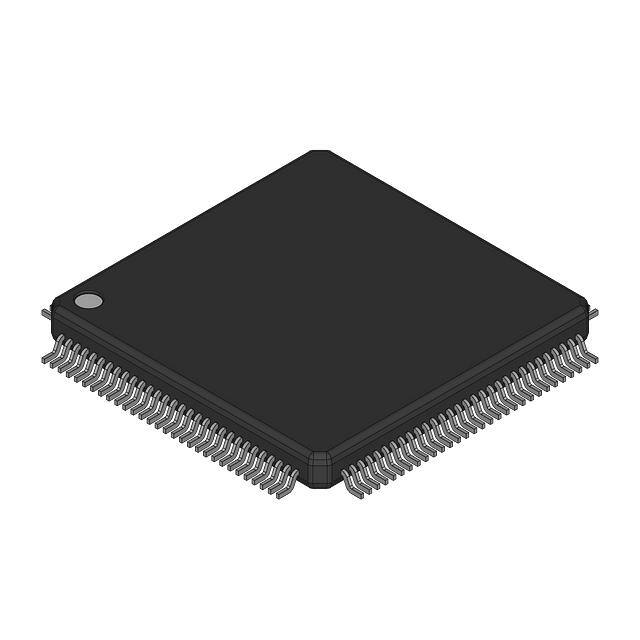
Package Diagram
120-pin Thin Quad Flatpack (14 x 14 x 1.4 mm) A120
51-85100
All product and company names mentioned in this document are the trademarks of their respective holders.
Document #: 38-06019 Rev. *B
Page 29 of 30
© Cypress Semiconductor Corporation, 2002. The information contained herein is subject to change without notice. Cypress Semiconductor Corporation assumes no responsibility for the use of any circuitry other than circuitry embodied in a Cypress Semiconductor product. Nor does it convey or imply any license under patent or other rights. Cypress Semiconductor does not authorize its products for use as critical components in life-support systems where a malfunction or failure may reasonably be expected to result in significant injury to the user. The inclusion of Cypress Semiconductor products in life-support systems application implies that the manufacturer assumes all risk of such use and in doing so indemnifies Cypress Semiconductor against all charges.
�CY7C43642 CY7C43662 CY7C43682
Document Title: CY7C43642, CY7C43662, CY7C43682 1K/4K/16K x36 x2 Bidirectional Synchronous FIFO Document Number: 38-06019 REV. ** *A *B ECN NO. 106556 117171 122271 Issue Date 06/08/01 08/23/02 12/26/02 Orig. of Change SZV OOR RBI Description of Change Change from Spec #: 38-00698 to 38-06019 Added footnote to retransmit timing Added note to retransmit section Power up requirements added to Maximum Ratings Information
Document #: 38-06019 Rev. *B
Page 30 of 30
�