CY7C66013C, CY7C66113C
Full Speed USB (12 Mbps) Peripheral Controller with Integrated Hub
Full Speed USB (12 Mbps) Peripheral Controller with Integrated Hub
Features
■
■ ■ ■ ■ ■ ■
Improved output drivers to reduce electromagnetic interference (EMI) Operating voltage from 4.0 V–5.5 V DC Operating temperature from 0 C–70 C CY7C66013C available in 48-pin SSOP (-PVXC) packages CY7C66113C available in 56-pin QFN or 56-pin SSOP (-PVXC) packages Industry standard programmer support
Full speed USB peripheral microcontroller with an integrated USB hub ❐ Well suited for USB compound devices such as a keyboard hub function 8-bit USB optimized microcontroller ❐ Harvard architecture ❐ 6 MHz external clock source ❐ 12 MHz internal CPU clock ❐ 48 MHz internal Hub clock Internal memory ❐ 256 bytes of RAM ❐ 8 kB of PROM Integrated Master and Slave I2C compatible controller (100 kHz) enabled through General Purpose I/O (GPIO) pins Hardware Assisted Parallel Interface (HAPI) for data transfer to external devices I/O ports ❐ Three GPIO ports (Port 0 to 2) capable of sinking 8 mA per pin (typical) ❐ An additional GPIO port (Port 3) capable of sinking 12 mA per pin (typical) for high current requirements: LEDs ❐ Higher current drive achievable by connecting multiple GPIO pins together to drive a common output ❐ Each GPIO port is configured as inputs with internal pull ups or open drain outputs or traditional CMOS outputs ❐ A Digital to Analog Conversion (DAC) port with programmable current sink outputs is available on the CY7C66113C device ❐ Maskable interrupts on all I/O pins 12-bit free running timer with one microsecond clock ticks Watchdog Timer (WDT) Internal Power on Reset (POR) USB Specification compliance ❐ Conforms to USB Specification, Version 1.1 ❐ Conforms to USB HID Specification, Version 1.1 ❐ Supports one or two device addresses with up to five user configured endpoints • Up to two 8-byte control endpoints • Up to four 8-byte data endpoints • Up to two 32-byte data endpoints ❐ Integrated USB transceivers ❐ Supports four downstream USB ports ❐ GPIO pins provide individual power control outputs for each downstream USB port ❐ GPIO pins provide individual port over current inputs for each downstream USB port
■
■
Functional Overview
The CY7C66013C and CY7C66113C are compound devices with a full speed USB microcontroller in combination with a USB hub. Each device is suited for combination peripheral functions with hubs such as a keyboard hub function. The 8-bit one time programmable microcontroller with a 12 Mbps USB Hub supports as many as four downstream ports.
■ ■ ■
GPIO
The CY7C66013C features 29 GPIO pins to support USB and other applications. The I/O pins are grouped into four ports (P0[7:0], P1[7:0], P2[7:0], P3[4:0]) where each port is configured as inputs with internal pull ups, open drain outputs, or traditional CMOS outputs. Ports 0 to 2 are rated at 8 mA per pin (typical) sink current. Port 3 pins are rated at 12 mA per pin (typical) sink current, which allows these pins to drive LEDs. Multiple GPIO pins are connected together to drive a single output for more drive current capacity. Additionally, each I/O pin is used to generate a GPIO interrupt to the microcontroller. All of the GPIO interrupts all share the same “GPIO” interrupt vector. The CY7C66113C has 31 GPIO pins (P0[7:0], P1[7:0], P2[7:0], P3[6:0]).
■ ■ ■ ■
DAC
The CY7C66113C has an additional port P4[7:0] that features an additional eight programmable sink current I/O pins (DAC). Every DAC pin includes an integrated 14 k pull up resistor. When a ‘1’ is written to a DAC I/O pin, the output current sink is disabled and the output pin is driven HIGH by the internal pull up resistor. When a ‘0’ is written to a DAC I/O pin, the internal pull up is disabled and the output pin provides the programmed amount of sink current. A DAC I/O pin is used as an input with an internal pull up by writing a ‘1’ to the pin. The sink current for each DAC I/O pin is individually programmed to one of sixteen values using dedicated Isink registers. DAC bits DAC[1:0] is used as high current outputs with a programmable sink current range of 3.2 to 16 mA (typical). DAC bits DAC[7:2] have a programmable current sink range of 0.2 to 1.0 mA (typical). Multiple DAC pins are connected together to drive a single output that requires more sink current capacity. Each I/O pin is used to generate a DAC interrupt to the microcontroller. Also, the interrupt polarity for each DAC I/O pin is individually programmable. • San Jose, CA 95134-1709 • 408-943-2600 Revised March 1, 2011
[+] Feedback
Cypress Semiconductor Corporation Document Number: 38-08024 Rev. *G
•
198 Champion Court
�CY7C66013C, CY7C66113C
Clock
The microcontroller uses an external 6 MHz crystal and an internal oscillator to provide a reference to an internal PLL based clock generator. This technology allows the customer application to use an inexpensive 6 MHz fundamental crystal that reduces the clock related noise emissions (EMI). A PLL clock generator provides the 6, 12, and 48 MHz clock signals for distribution within the microcontroller.
Interrupts
The microcontroller supports eleven maskable interrupts in the vectored interrupt controller. Interrupt sources include the 128 s (bit 6) and 1.024 ms (bit 9) outputs from the free-running timer, five USB endpoints, the USB hub, the DAC port, the GPIO ports, and the I2C compatible master mode interface. The timer bits cause an interrupt (if enabled) when the bit toggles from LOW ‘0’ to HIGH ‘1.’ The USB endpoints interrupt after the USB host has written data to the endpoint FIFO or after the USB controller sends a packet to the USB host. The DAC ports have an additional level of masking that allows the user to select which DAC inputs causes a DAC interrupt. The GPIO ports also have a level of masking to select which GPIO inputs causes a GPIO interrupt. For additional flexibility, the input transition polarity that causes an interrupt is programmable for each pin of the DAC port. Input transition polarity is programmed for each GPIO port as part of the port configuration. The interrupt polarity can be rising edge (‘0’ to ‘1’) or falling edge (‘1’ to ‘0’).
Memory
The CY7C66013C and CY7C66113C have 8 kB of PROM.
Power on Reset, Watchdog, and Free Running Timer
These parts include POR logic, a WDT, and a 12-bit free-running timer. The POR logic detects when power is applied to the device, resets the logic to a known state, and begins executing instructions at PROM address 0x0000. The WDT is used to ensure that the microcontroller recovers after a period of inactivity. The firmware may become inactive for a variety of reasons, including errors in the code or a hardware failure such as waiting for an interrupt that never occurs.
USB
The CY7C66013C and CY7C66113C include an integrated USB Serial Interface Engine (SIE) that supports the integrated peripherals and the hub controller function. The hardware supports up to two USB device addresses with one device address for the hub (two endpoints) and a device address for a compound device (three endpoints). The SIE allows the USB host to communicate with the hub and functions integrated into the microcontroller. The part includes a 1:4 hub repeater with one upstream port and four downstream ports. The USB Hub allows power management control of the downstream ports by using GPIO pins assigned by the user firmware. The user has the option of ganging the downstream ports together with a single pair of power management pins, or providing power management for each port with four pairs of power management pins.
I2C and HAPI Interface
The microcontroller communicates with external electronics through the GPIO pins. An I2C compatible interface accommodates a 100 kHz serial link with an external device. There is also a HAPI to transfer data to an external device.
Timer
The free-running 12-bit timer clocked at 1 MHz provides two interrupt sources, 128 s and 1.024 ms. The timer is used to measure the duration of an event under firmware control by reading the timer at the start of the event and after the event is complete. The difference between the two readings indicates the duration of the event in microseconds. The upper four bits of the timer are latched into an internal register when the firmware reads the lower eight bits. A read from the upper four bits actually reads data from the internal register, instead of the timer. This feature eliminates the need for firmware to try to compensate if the upper four bits increment immediately after the lower eight bits are read.
Document Number: 38-08024 Rev. *G
Page 2 of 61
[+] Feedback
�CY7C66013C, CY7C66113C
Logic Block Diagram
External 6 MHz crystal USB Transceiver
D+[0] Upstream D–[0] USB Port
PLL USB Transceiver
D+[1] D–[1]
48 MHz Clock Divider 12 MHz PROM 8 KB 8-bit Bus USB SIE 12 MHz 8-bit CPU Repeater
USB Transceiver
D+[2] D–[2]
USB Transceiver
D+[3] D–[3]
RAM 256 byte
Interrupt Controller
USB Transceiver
D+[4] D–[4]
Downstream USB Ports
6 MHz
12-bit Timer
GPIO PORT 0
P0[0] P0[7] P1[0] P1[7] P2[0:1,7] P2[2]; Latch_Empty P2[3]; Data_Ready P2[4]; STB P2[5]; OE P2[6]; CS P3[0] P3[4]
Power management under firmware control using GPIO pins
Watchdog Timer
GPIO PORT 1
Power-On Reset
GPIO/ HAPI PORT 2
GPIO PORT 3 GPIO PORT 3 DAC PORT I2C Interface
High Current Outputs
P3[5] Additional P3[6] High Current Outputs DAC[0] DAC[7] CY7C66113C only SCLK SDATA
*I2C-compatible interface enabled by firmware through P2[1:0] or P1[1:0]
Document Number: 38-08024 Rev. *G
Page 3 of 61
[+] Feedback
�CY7C66013C, CY7C66113C
Contents
Pin Configurations ........................................................... 5 Product Summary Tables ................................................ 9 Pin Assignments .......................................................... 9 I/O Register Summary ................................................. 9 Instruction Set Summary ........................................... 11 Programming Model ....................................................... 12 14-bit Program Counter (PC) .................................... 12 8-bit Accumulator (A) ................................................. 13 8-bit Temporary Register (X) ..................................... 13 8-bit Program Stack Pointer (PSP) ............................ 13 8-bit Data Stack Pointer (DSP) .................................. 13 Address Modes ......................................................... 14 Clocking .......................................................................... 14 Reset ................................................................................ 15 Power on Reset ......................................................... 15 Watchdog Reset ........................................................ 15 Suspend Mode ................................................................ 16 General Purpose I/O (GPIO) Ports ................................ 16 GPIO Configuration Port ........................................... 18 GPIO Interrupt Enable Ports ..................................... 19 DAC Port .......................................................................... 20 DAC Isink Registers .................................................. 21 DAC Port Interrupts ................................................... 21 12-bit Free-Running Timer ............................................. 22 I2C and HAPI Configuration Register ........................... 23 I2C Compatible Controller .............................................. 23 Hardware Assisted Parallel Interface (HAPI) ............... 26 Processor Status and Control Register ....................... 27 Interrupts ......................................................................... 28 Interrupt Vectors ........................................................ 29 Interrupt Latency ....................................................... 30 USB Bus Reset Interrupt ........................................... 30 Timer Interrupt ........................................................... 30 USB Endpoint Interrupts ............................................ 30 USB Hub Interrupt ..................................................... 30 DAC Interrupt ............................................................ 31 GPIO and HAPI Interrupt ........................................... 31 I2C Interrupt ............................................................... 32 USB Overview ................................................................. 32 USB Serial Interface Engine ...................................... 32 USB Enumeration ...................................................... 32 USB Hub .......................................................................... 33 Connecting and Disconnecting a USB Device .......... 33 Enabling and Disabling a USB Device ...................... 34 Hub Downstream Ports Status and Control .............. 35 Downstream Port Suspend and Resume .................. 36 USB Upstream Port Status and Control .................... 38 USB SIE Operation ......................................................... 39 USB Device Addresses ............................................. 39 USB Device Endpoints .............................................. 39 USB Control Endpoint Mode Registers ..................... 39 USB Non Control Endpoint Mode Registers ............. 41 USB Endpoint Counter Registers .............................. 41 Endpoint Mode and Count Registers Update and Locking Mechanism .......................................................... 42 USB Mode Tables ........................................................... 44 Register Summary .......................................................... 48 Sample Schematic .......................................................... 50 Absolute Maximum Ratings .......................................... 51 Electrical Characteristics ............................................... 51 Switching Characteristics .............................................. 52 Ordering Information ...................................................... 55 Ordering Code Definitions ......................................... 55 Package Diagrams .......................................................... 56 Quad Flat Package No Leads (QFN) Package Design Notes ................................................................... 58 Acronyms ........................................................................ 59 Document Conventions ................................................. 59 Units of Measure ....................................................... 59 Document History Page ................................................. 60 Sales, Solutions, and Legal Information ...................... 61 Worldwide Sales and Design Support ....................... 61 Products .................................................................... 61 PSoC Solutions ......................................................... 61
Document Number: 38-08024 Rev. *G
Page 4 of 61
[+] Feedback
�CY7C66013C, CY7C66113C
Pin Configurations
Figure 1. CY7C66013C 48-pin SSOP and CY7C66113C 56-pin SSOP TOP VIEW CY7C66013C
XTALOUT XTALIN VREF P1[3] P1[5] P1[7] P3[1] D+[0] D–[0] P3[3] GND D+[1] D–[1] P2[1] D+[2] D–[2] P2[3] P2[5] P2[7] GND P0[7] P0[5] P0[3] P0[1] 1 2 3 4 5 6 7 8 9 10 11 12 13 14 15 16 17 18 19 20 21 22 23 24 48 47 46 45 44 43 42 41 40 39 38 37 36 35 34 33 32 31 30 29 28 27 26 25 VCC P1[1] P1[0] P1[2] P1[4] P1[6] P3[0] D–[3] D+[3] P3[2] GND P3[4] D–[4] D+[4] P2[0] P2[2] GND P2[4] P2[6] VPP P0[0] P0[2] P0[4] P0[6] XTALOUT XTALIN VREF P1[3] P1[5] P1[7] P3[1] D+[0] D–[0] P3[3] GND P3[5] D+[1] D–[1] P2[1] D+[2] D–[2] P2[3] P2[5] P2[7] DAC[7] P0[7] P0[5] P0[3] P0[1] DAC[5] DAC[3] DAC[1]
CY7C66113C
1 2 3 4 5 6 7 8 9 10 11 12 13 14 15 16 17 18 19 20 21 22 23 24 25 26 27 28 56 55 54 53 52 51 50 49 48 47 46 45 44 43 42 41 40 39 38 37 36 35 34 33 32 31 30 29 VCC P1[1] P1[0] P1[2] P1[4] P1[6] P3[0] D–[3] D+[3] P3[2] P3[4] D–[4] D+[4] P3[6] P2[0] P2[2] GND P2[4] P2[6] DAC[0] VPP P0[0] P0[2] P0[4] P0[6] DAC[2] DAC[4] DAC[6]
Document Number: 38-08024 Rev. *G
Page 5 of 61
[+] Feedback
�CY7C66013C, CY7C66113C
Figure 2. CY7C66113C 56-pin QFN
XTALOUT
XTALIN
D+[0]
56
P1[1]
P1[0]
P1[2]
P1[4]
P1[6]
P3[1]
55
P1[7]
54
P1[5]
53
P1[3]
52
Vref
51
Vcc
50
49
48
47
46
45
44
43
D-[0] P3[3] GND P3[5] D+[1] D–[1] P2[1] D+[2] D–[2] P2[3] P2[5] P2[7] DAC[7] P0[7]
1 2 3 4 5 6 7 8 9 10 11 12 13 14 15 16 17 18 19 20 21 22 23 24 25 26 27 28
42 41 40 39 38
P3[0] D–[3] D+[3] P3[2] P3[4] D–[4] D+[4] P3[6] P2[0] P2[2] GND P2[4] P2[6] DAC[0]
CY7C66113C 56-pin QFN
37 36 35 34 33 32 31 30 29
Document Number: 38-08024 Rev. *G
P0[5]
P0[3]
P0[1]
DAC[5]
DAC[3]
DAC[1]
DAC[6]
DAC[4]
DAC[2]
P0[6]
P0[4]
P0[2]
P0[0]
Vpp
Page 6 of 61
[+] Feedback
�CY7C66013C, CY7C66113C
Figure 3. CY7C66113C DIE
(3398, 4194)
Cypress Logo
Pin 1
Pin 60 Pin 15
Pin 30
Pin 45
(0,0) DIE STEP: 3398 x 4194 microns Die Size: 3322 x 4129 microns Die Thickness: 14 mils = 355.6 microns Pad Size: 80 x 80 microns
Document Number: 38-08024 Rev. *G
Page 7 of 61
[+] Feedback
�CY7C66013C, CY7C66113C
Table 1. Pad Coordinates in Microns (0,0) to Bond Pad Centers Pad No. 1 2 3 4 5 6 7 8 9 10 11 12 13 14 15 16 17 18 19 20 21 22 23 24 25 26 27 28 29 30 31 32 33 34 35 36 Pin Name XtalOut XtalIn Vref Port11b Port13 Port15 Vss Port17 Port31 Du+ Du– Port33 Vss Port35 DD+1 DD–1 Port37 Vref Port21 DD+2 DD–2 Port23 Vss Port25 DD+7 DD–7 Port27 DAC7 Vss Port07 Port05 Port03 Port01 DAC5 DAC3 DAC1 X 1274.2 1132.8 889.85 684.65 581.65 478.65 375.65 0 0 0 0 0 0 0 0 0 0 0 0 0 0 0 0 0 0 0 0 0 0 375.2 478.2 581.2 684.2 788.4 891.4 994.4 Y 3588.8 3588.8 3588.8 3588.8 3588.8 3588.8 3588.8 3408.35 3162.05 3060.55 2752.4 2650.95 2474.6 2368.45 2266.95 1958.85 1857.35 1680.4 1567.4 1465.95 1157.85 1056.35 880 773.85 672.35 364.25 262.75 100.75 0 210.6 210.6 210.6 210.6 210.6 210.6 210.6 Pad # 37 38 39 40 41 42 43 44 45 46 47 48 49 50 51 52 53 54 55 56 57 58 59 60 61 62 63 64 65 66 67 68 69 70 71 Pin Name DAC6 DAC4 DAC2 Port06 Port04 Port02 Port00 Vpp DAC0 Port26 DD+6 DD–6 Port24 Vss Port22 DD+5 DD–5 Port20 Vref Port36 DD+4 DD–4 Port34 Vss Port32 DD+3 DD–3 Port30 Port16 Port14 Port12 Port10 Port11 VCC PadOpt X 2000.6 2103.6 2206.6 2308.4 2411.4 2514.4 2617.4 2992.4 2992.4 2992.4 2992.4 2992.4 2992.4 2992.4 2992.4 2992.4 2992.4 2992.4 2992.4 2992.4 2992.4 2992.4 2992.4 2992.4 2992.4 2992.4 2992.4 2992.4 2992.4 2634.2 2531.2 2428.2 2325.2 2221.75 2121.75 Y 210.6 210.6 210.6 210.6 210.6 210.6 210.6 25.4 151.75 306.15 407.65 715.75 817.25 923.4 1086.75 1188.25 1496.35 1597.85 1710.8 1874.75 1976.25 2284.35 2385.85 2492 2655.35 2756.85 3064.95 3166.45 3412.25 3588.8 3588.8 3588.8 3588.8 3588.8 3588.8
Document Number: 38-08024 Rev. *G
Page 8 of 61
[+] Feedback
�CY7C66013C, CY7C66113C
Product Summary Tables
Pin Assignments
Table 2. Pin Assignments Name D+[0], D–[0] D+[1], D–[1] D+[2], D–[2] D+[3], D–[3] D+[4], D–[4] P0[7:0] P1[7:0] P2[7:0] P3[6:0] DAC[7:0] I/O I/O I/O I/O I/O I/O I/O I/O I/O I/O I/O 8, 9 12, 13 15, 16 40, 41 35, 36 21, 25, 22, 26, 23, 27, 24, 28 6, 43, 5, 44, 4, 45, 47, 46 19, 30, 18, 31, 17, 33, 14, 34 48-pin 56-pin QFN 56, 1 5, 6 8, 9 40, 41 36, 37 56-pin SSOP 8, 9 13, 14 16, 17 48, 49 44, 45 Description Upstream port, USB differential data. Downstream port 1, USB differential data. Downstream port 2, USB differential data. Downstream port 3, USB differential data. Downstream port 4, USB differential data.
14, 15, 16, 17, 22, 32, 23, 33, GPIO Port 0. 24, 25, 26, 27 24, 34, 25, 35 52, 53, 54, 43, 6, 51, 5, 52, 4, GPIO Port 1. 44, 45, 46, 47 53, 55, 54 7, 10, 11, 12, 20, 38, 19, 39, GPIO Port 2. 30, 31, 33, 34 18, 41, 15, 42 43, 12, 46, 10, GPIO Port 3, capable of sinking 12 mA (typical). 47, 7, 50
37, 10, 39, 7, 42 55, 2, 4, 35, 38, 39, 42, n/a
13, 18, 19, 20, 21, 29, 26, 30, Digital to Analog Converter (DAC) Port with programmable 21, 22, 23, 29 27, 31, 28, 37 current sink outputs. DAC[1:0] offer a programmable range of 3.2 to 16 mA typical. DAC[7:2] have a programmable sink current range of 0.2 to 1.0 mA typical. 50 49 28 48 3, 32 51 2 1 36 56 11, 40 3 6 MHz crystal or external clock input. 6 MHz crystal out. Programming voltage supply, tie to ground during normal operation. Voltage supply. Ground. External 3.3 V supply voltage for the differential data output buffers and the D+ pull up.
XTALIN XTALOUT VPP VCC GND VREF
IN
2 29 48 11, 20, 32, 38
OUT 1
IN
3
I/O Register Summary
I/O registers are accessed via the I/O Read (IORD) and I/O Write (IOWR, IOWX) instructions. IORD reads data from the selected port into the accumulator. IOWR performs the reverse; it writes data from the accumulator to the selected port. Indexed I/O Write (IOWX) adds the contents of X to the address in the instruction to form the port address and writes data from the accumulator to the specified port. Specifying address 0 such as IOWX 0h indicates the I/O register is selected solely by the contents of X. All undefined registers are reserved. It is important not to write to reserved registers as this may cause an undefined operation or increased current consumption during operation. When writing to registers with reserved bits, the reserved bits must be written with ‘0.’ Table 3. I/O Register Summary Register Name Port 0 Data Port 1 Data Port 2 Data Port 3 Data Port 0 Interrupt Enable Port 1 Interrupt Enable Port 2 Interrupt Enable Port 3 Interrupt Enable GPIO Configuration Document Number: 38-08024 Rev. *G I/O Address 0x00 0x01 0x02 0x03 0x04 0x05 0x06 0x07 0x08 Read/Write R/W R/W R/W R/W W W W W R/W GPIO Port 0 Data GPIO Port 1 Data GPIO Port 2 Data GPIO Port 3 Data Interrupt Enable for Pins in Port 0 Interrupt Enable for Pins in Port 1 Interrupt Enable for Pins in Port 2 Interrupt Enable for Pins in Port 3 GPIO Port Configurations Function Page 16 17 17 17 19 19 19 19 18 Page 9 of 61
[+] Feedback
�CY7C66013C, CY7C66113C
Table 3. I/O Register Summary (continued) Register Name HAPI and I C Configuration USB Device Address A EP A0 Counter Register EP A0 Mode Register EP A1 Counter Register EP A1 Mode Register EP A2 Counter Register EP A2 Mode Register USB Status & Control Global Interrupt Enable Endpoint Interrupt Enable Interrupt Vector Timer (LSB) Timer (MSB) WDT Clear I2C Control & Status I2C Data DAC Data DAC Interrupt Enable DAC Interrupt Polarity DAC Isink USB Device Address B EP B0 Counter Register EP B0 Mode Register EP B1 Counter Register EP B1 Mode Register Hub Port Connect Status Hub Port Enable Hub Port Speed Hub Port Control (Ports [4:1]) Hub Port Suspend Hub Port Resume Status Hub Ports SE0 Status Hub Ports Data Hub Downstream Force Low Processor Status & Control
2
I/O Address 0x09 0x10 0x11 0x12 0x13 0x14 0x15 0x16 0x1F 0x20 0x21 0x23 0x24 0x25 0x26 0x28 0x29 0x30 0x31 0x32 0x38-0x3F 0x40 0x41 0x42 0x43 0x44 0x48 0x49 0x4A 0x4B 0x4D 0x4E 0x4F 0x50 0x51 0xFF
Read/Write R/W R/W R/W R/W R/W R/W R/W R/W R/W R/W R/W R R R W R/W R/W R/W W W W R/W R/W R/W R/W R/W R/W R/W R/W R/W R/W R R R R/W R/W
2
Function HAPI Width and I C Position Configuration USB Device Address A USB Address A, Endpoint 0 Counter USB Address A, Endpoint 0 Configuration USB Address A, Endpoint 1 Counter USB Address A, Endpoint 1 Configuration USB Address A, Endpoint 2 Counter USB Address A, Endpoint 2 Configuration USB Upstream Port Traffic Status and Control Global Interrupt Enable USB Endpoint Interrupt Enables Pending Interrupt Vector Read/Clear Lower 8 Bits of Free-running Timer (1 MHz) Upper 4 Bits of Free-running Timer Watchdog Timer Clear I2C Status and Control I2C Data DAC Data Interrupt Enable for each DAC Pin Interrupt Polarity for each DAC Pin Input Sink Current Control for each DAC Pin USB Device Address B (not used in 5-endpoint mode) USB Address B, Endpoint 0 Counter USB Address B, Endpoint 0 Configuration, or USB Address A, Endpoint 3 in 5-endpoint Mode USB Address B, Endpoint 1 Counter USB Address B, Endpoint 1 Configuration, or USB Address A, Endpoint 4 in 5-endpoint Mode Hub Downstream Port Connect Status Hub Downstream Ports Enable Hub Downstream Ports Speed Hub Downstream Ports Control Hub Downstream Port Suspend Control Hub Downstream Ports Resume Status Hub Downstream Ports SE0 Status Hub Downstream Ports Differential Data Hub Downstream Ports Force LOW Microprocessor Status and Control Register
Page 23 39 41 40 41 41 41 41 38 28 28 30 22 22 15 24 24 20 21 21 21 39 41 40 41 41 33 34 34 35 36 37 36 36 35 27
Document Number: 38-08024 Rev. *G
Page 10 of 61
[+] Feedback
�CY7C66013C, CY7C66113C
Instruction Set Summary
Refer to the CYASM Assembler User’s Guide for more details. Table 4. Instruction Set Summary Mnemonic HALT ADD A,expr ADD A,[expr] ADD A,[X+expr] ADC A,expr ADC A,[expr] ADC A,[X+expr] SUB A,expr SUB A,[expr] SUB A,[X+expr] SBB A,expr SBB A,[expr] SBB A,[X+expr] OR A,expr OR A,[expr] OR A,[X+expr] AND A,expr AND A,[expr] AND A,[X+expr] XOR A,expr XOR A,[expr] XOR A,[X+expr] CMP A,expr CMP A,[expr] CMP A,[X+expr] MOV A,expr MOV A,[expr] MOV A,[X+expr] MOV X,expr MOV X,[expr] reserved XPAGE MOV A,X MOV X,A MOV PSP,A CALL JMP CALL JZ JNZ addr addr addr addr addr data direct index data direct index data direct index data direct index data direct index data direct index data direct index data direct index data direct index data direct Operand Opcode 00 01 02 03 04 05 06 07 08 09 0A 0B 0C 0D 0E 0F 10 11 12 13 14 15 16 17 18 19 1A 1B 1C 1D 1E 1F 40 41 60 50-5F 80-8F 90-9F A0-AF B0-BF 4 4 4 4 10 5 10 5 5 7 4 6 7 4 6 7 4 6 7 4 6 7 4 6 7 4 6 7 4 6 7 5 7 8 4 5 6 4 5 Cycles Mnemonic NOP INC A INC X INC [expr] INC [X+expr] DEC A DEC X DEC [expr] DEC [X+expr] IORD expr IOWR expr POP A POP X PUSH A PUSH X SWAP A,X SWAP A,DSP MOV [expr],A MOV [X+expr],A OR [expr],A OR [X+expr],A AND [expr],A AND [X+expr],A XOR [expr],A XOR [X+expr],A IOWX [X+expr] CPL ASL ASR RLC RRC RET DI EI RETI JC JNC JACC INDEX addr addr addr addr direct index direct index direct index direct index index acc x direct index acc x direct index address address Operand Opcode 20 21 22 23 24 25 26 27 28 29 2A 2B 2C 2D 2E 2F 30 31 32 33 34 35 36 37 38 39 3A 3B 3C 3D 3E 3F 70 72 73 C0-CF D0-DF E0-EF F0-FF 4 4 4 7 8 4 4 7 8 5 5 4 4 5 5 5 5 5 6 7 8 7 8 7 8 6 4 4 4 4 4 8 4 4 8 5 5 7 14 Cycles
Document Number: 38-08024 Rev. *G
Page 11 of 61
[+] Feedback
�CY7C66013C, CY7C66113C
Programming Model
14-bit Program Counter (PC)
The 14-bit PC allows access to up to 8 kB of PROM available with the CY7C66x13C architecture. The top 32 bytes of the ROM in the 8K part are reserved for testing purposes. The program counter is cleared during reset, such that the first instruction executed after a reset is at address 0x0000h. Typically, this is a jump instruction to a reset handler that initializes the application (see Interrupt Vectors on page 29). The lower eight bits of the program counter are incremented as instructions are loaded and executed. The upper six bits of the program counter are incremented by executing an XPAGE instruction. The last instruction executed within a 256-byte “page” of sequential code should be an XPAGE instruction. The assembler directive “XPAGEON” causes the assembler to insert XPAGE instructions automatically. Because instructions are either one or two bytes long, the assembler may occasionally need to insert a NOP followed by an XPAGE to execute correctly. The address of the next instruction to be executed, the carry flag, and the zero flag are saved as two bytes on the program stack during an interrupt acknowledge or a CALL instruction. The program counter, carry flag, and zero flag are restored from the program stack during a RETI instruction. Only the program counter is restored during a RET instruction. The program counter is not accessed directly by the firmware. The program stack is examined by reading SRAM from location 0x00 and up. Program Memory Organization Table 5. Program Memory Space with Interrupt Vector Table
After Reset Address
14-bit PC
0x0000 0x0002 0x0004 0x0006 0x0008
Program execution begins here after a reset USB bus reset interrupt vector 128 s timer interrupt vector 1.024 ms timer interrupt vector USB address A endpoint 0 interrupt vector
0x000A USB address A endpoint 1 interrupt vector 0x000C USB address A endpoint 2 interrupt vector 0x000E 0x0010 0x0012 0x0014 0x0016 0x0018 USB address B endpoint 0 interrupt vector USB address B endpoint 1 interrupt vector Hub interrupt vector DAC interrupt vector GPIO/HAPI interrupt vector I2C interrupt vector
0x001A Program Memory begins here
0x1FDF 8 kB (-32) PROM ends here.
Document Number: 38-08024 Rev. *G
Page 12 of 61
[+] Feedback
�CY7C66013C, CY7C66113C
8-bit Accumulator (A)
The accumulator is the general purpose register for the microcontroller. counter and flags on the program “stack” and increment the PSP by two. The Return From Interrupt (RETI) instruction decrements the PSP, then restores the second byte from memory addressed by the PSP. The PSP is decremented again and the first byte is restored from memory addressed by the PSP. After the program counter and flags are restored from stack, the interrupts are enabled. The overall effect is to restore the program counter and flags from the program stack, decrement the PSP by two, and re-enable interrupts. The Call Subroutine (CALL) instruction stores the program counter and flags on the program stack and increments the PSP by two. The Return From Subroutine (RET) instruction restores the program counter but not the flags from the program stack and decrements the PSP by two. Data Memory Organization The CY7C66x13C microcontrollers provide 256 bytes of data RAM. Normally, the SRAM is partitioned into four areas: program stack, user variables, data stack, and USB endpoint FIFOs. The following is one example of where the program stack, data stack, and user variables areas are located.
8-bit Temporary Register (X)
The “X” register is available to the firmware for temporary storage of intermediate results. The microcontroller performs indexed operations based on the value in X. Refer to the section, Indexed on page 14 for additional information.
8-bit Program Stack Pointer (PSP)
During a reset, the Program Stack Pointer (PSP) is set to 0x00 and “grows” upward from this address. The PSP may be set by firmware, using the MOV PSP,A instruction. The PSP supports interrupt service under hardware control and CALL, RET, and RETI instructions under firmware control. The PSP is not readable by the firmware. During an interrupt acknowledge, interrupts are disabled and the 14-bit program counter, carry flag, and zero flag are written as two bytes of data memory. The first byte is stored in the memory addressed by the PSP, then the PSP is incremented. The second byte is stored in memory addressed by the PSP, and the PSP is incremented again. The overall effect is to store the program Table 6. SRAM Areas After Reset
8-bit DSP (Move DSP[1]) 8-bit PSP
Address
0x00
Program Stack Growth
8-bit DSP
User Selected
Data Stack Growth User variables
USB FIFO space for up to two addresses and five endpoints[2]
0xFF
8-bit Data Stack Pointer (DSP)
The Data Stack Pointer (DSP) supports PUSH and POP instructions that use the data stack for temporary storage. A PUSH instruction pre-decrements the DSP, then writes data to the memory location addressed by the DSP. A POP instruction reads data from the memory location addressed by the DSP, then post-increments the DSP. During a reset, the DSP is reset to 0x00. A PUSH instruction when DSP equals 0x00 writes data at the top of the data RAM (address 0xFF). This writes data to the memory area reserved for USB endpoint FIFOs. Therefore, the DSP should be indexed at an appropriate memory location that does not compromise the
Program Stack, user defined memory (variables), or the USB endpoint FIFOs. For USB applications, the firmware should set the DSP to an appropriate location to avoid a memory conflict with RAM dedicated to USB FIFOs. The memory requirements for the USB endpoints are described in USB Device Endpoints on page 39. Example assembly instructions to do this with two device addresses (FIFOs begin at 0xD8) are shown:
■ ■
MOV A,20h; Move 20 hex into Accumulator (must be D8h or less) SWAP A,DSP; swap accumulator value into DSP register.
Notes 1. Refer to 8-bit Data Stack Pointer (DSP) for a description of DSP. 2. Endpoint sizes are fixed by the Endpoint Size Bit (I/O register 0x1F, Bit 7), see Table 47.
Document Number: 38-08024 Rev. *G
Page 13 of 61
[+] Feedback
�CY7C66013C, CY7C66113C
Address Modes
The CY7C66013C and CY7C66113C microcontrollers support three addressing modes for instructions that require data operands: data, direct, and indexed. Data (Immediate) “Data” address mode refers to a data operand that is actually a constant encoded in the instruction. As an example, consider the instruction that loads A with the constant 0xD8: MOV A, 0D8h. This instruction requires two bytes of code where the first byte identifies the “MOV A” instruction with a data operand as the second byte. The second byte of the instruction is the constant “0xD8”. A constant may be referred to by name if a prior “EQU” statement assigns the constant value to the name. For example, the following code is equivalent to the example described earlier: DSPINIT: EQU 0D8h MOV A, DSPINIT. Direct “Direct” address mode is used when the data operand is a variable stored in SRAM. In that case, the one byte address of the variable is encoded in the instruction. As an example, consider an instruction that loads A with the contents of memory address location 0x10: MOV A, [10h]. Normally, variable names are assigned to variable addresses using “EQU” statements to improve the readability of the assembler source code. As an example, the following code is equivalent to the example described earlier: buttons: EQU 10h MOV A, [buttons]. Indexed “Indexed” address mode allows the firmware to manipulate arrays of data stored in SRAM. The address of the data operand is the sum of a constant encoded in the instruction and the contents of the “X” register. Normally, the constant is the “base” address of an array of data and the X register contains an index that indicates which element of the array is actually addressed: array: EQU 10h MOV X, 3 MOV A, [X+array]. This has the effect of loading A with the fourth element of the SRAM “array” that begins at address 0x10. The fourth element would be at address 0x13.
Clocking
Figure 4. Clock Oscillator On-Chip Circuit XTALOUT (pin 1)
XTALIN (pin 2) 30 pF
To Internal PLL 30 pF
The XTALIN and XTALOUT are the clock pins to the microcontroller. The user connects an external oscillator or a crystal to these pins. When using an external crystal, keep PCB traces between the chip leads and crystal as short as possible (less than 2 cm). A 6 MHz fundamental frequency parallel resonant crystal is connected to these pins to provide a reference frequency for the internal PLL. The two internal 30 pF load caps appear in series to the external crystal and would be equivalent to a 15 pF load. Therefore, the crystal must have a required load capacitance of about 15–18 pF. A ceramic resonator does not allow the microcontroller to meet the timing specifications of full speed USB and so a ceramic resonator is not recommended with these parts. An external 6 MHz clock is applied to the XTALIN pin if the XTALOUT pin is left open. Grounding the XTALOUT pin when driving XTALIN with an oscillator does not work because the internal clock is effectively shorted to ground.
Document Number: 38-08024 Rev. *G
Page 14 of 61
[+] Feedback
�CY7C66013C, CY7C66113C
Reset
The CY7C66x13C supports two resets: POR and a Watchdog Reset (WDR). Each of these resets causes:
■ ■ ■ ■
All registers to be restored to their default states. The USB device addresses to be set to 0. All interrupts to be disabled. The PSP and DSP to be set to memory address 0x00.
not interruptible, and the semi-suspend state continues for an additional 95 ms unless the count is bypassed by a USB Bus Reset on the upstream port. The 95 ms provides time for VCC to stabilize at a valid operating voltage before the chip executes code. If a USB Bus Reset occurs on the upstream port during the 95 ms semi-suspend time, the semi-suspend state is aborted and program execution begins immediately from address 0x0000. In this case, the Bus Reset interrupt is pending but not serviced until firmware sets the USB Bus Reset Interrupt Enable bit (bit 0 of register 0x20) and enables interrupts with the EI command. The POR signal is asserted whenever VCC drops below approximately 2.5 V, and remains asserted until VCC rises above this level again. Behavior is the same as described earlier.
The occurrence of a reset is recorded in the Processor Status and Control Register, as described in Processor Status and Control Register on page 27. Bits 4 and 6 are used to record the occurrence of POR and WDR, respectively. Firmware interrogates these bits to determine the cause of a reset. Program execution starts at ROM address 0x0000 after a reset. Although this looks similar to interrupt vector 0, there is an important difference. Reset processing does NOT push the program counter, carry flag, and zero flag onto program stack. The firmware reset handler should configure the hardware before the “main” loop of code. Attempting to execute a RET or RETI in the firmware reset handler causes unpredictable execution results.
Watchdog Reset
The WDR occurs when the internal WDT rolls over. Writing any value to the write only Watchdog Restart Register at address 0x26 clears the timer. The timer rolls over and WDR occurs if it is not cleared within tWATCH (8 ms minimum) of the last clear. Bit 6 of the Processor Status and Control Register is set to record this event (the register contents are set to 010X0001 by the WDR). A WDT Reset lasts for 2 ms, after which the microcontroller begins execution at ROM address 0x0000. The USB transmitter is disabled by a WDR because the USB Device Address Registers are cleared (see USB Device Addresses on page 39). Otherwise, the USB Controller responds to all address 0 transactions. It is possible to set the WDR bit of the Processor Status and Control Register (0xFF) following a POR event. If a firmware interrogates the Processor Status and Control Register for a set condition on the WDR bit, the WDR bit should be ignored if the POR (bit 3 of register 0xFF) bit is set.
Power on Reset
When VCC is first applied to the chip, the POR signal is asserted and the CY7C66x13C enters a “semi-suspend” state. During the semi-suspend state, which is different from the suspend state defined in the USB specification, the oscillator and all other blocks of the part are functional, except for the CPU. This semi-suspend time ensures that both a valid VCC level is reached and that the internal PLL has time to stabilize before full operation begins. When the VCC rises above approximately 2.5 V, and the oscillator is stable, the POR is deasserted and the on-chip timer starts counting. The first 1 ms of suspend time is
Figure 5. Watchdog Reset tWATCH 2 ms
Last write to WDT Register
No write to WDT register, so WDR goes HIGH
Execution begins at Reset Vector 0x0000
Document Number: 38-08024 Rev. *G
Page 15 of 61
[+] Feedback
�CY7C66013C, CY7C66113C
Suspend Mode
The CY7C66x13C is placed into a low power state by setting the Suspend bit of the Processor Status and Control register. All logic blocks in the device are turned off except the GPIO interrupt logic and the USB receiver. The clock oscillator, PLL, and the free-running and WDTs are shut down. Only the occurrence of an enabled GPIO interrupt or non idle bus activity at a USB upstream or downstream port wakes the part from suspend. The Run bit in the Processor Status and Control Register must be set to resume a part out of suspend. The clock oscillator restarts immediately after exiting suspend mode. The microcontroller returns to a fully functional state 1 ms after the oscillator is stable. The microcontroller executes the instruction following the I/O write that placed the device into suspend mode before servicing any interrupt requests. The GPIO interrupt allows the controller to wake up periodically and poll system components while maintaining a very low average power consumption. To achieve the lowest possible current during suspend mode, all I/O should be held at VCC or Gnd. This also applies to internal port pins that may not be bonded in a particular package. Typical code for entering suspend is given here: ... ; All GPIO set to low power state (no floating pins) ... ; Enable GPIO interrupts if desired for wakeup mov a, 09h; Set suspend and run bits iowr FFh; Write to Status and Control Register – Enter suspend, wait for USB activity (or GPIO Interrupt) nop ; This executes before any ISR
General Purpose I/O (GPIO) Ports
Figure 6. Block Diagram of a GPIO Pin
GPIO CFG OE
VCC
mode 2-bits Q1 Control Data Out Latch Q2
Internal Data Bus Port Write
14 k GPIO PIN
Port Read
Data In Latch Control
Q3*
Reg_Bit STRB
(Latch is Transparent except in HAPI mode)
Data Interrupt Latch
Interrupt Enable Interrupt Controller
*Port 0,1,2: Low Isink Port 3: High Isink
There are up to 31 GPIO pins (P0[7:0], P1[7:0], P2[7:0], and P3[6:0]) for the hardware interface. The number of GPIO pins changes based on the package type of the chip. Each port is configured as inputs with internal pull ups, open drain outputs, or traditional CMOS outputs. Port 3 offers a higher current drive, with typical current sink capability of 12 mA. The data for each GPIO port is accessible through the data registers. Port data registers are shown in Table 7 on page 17 through Table 10 on page 17, and are set to 1 on reset.
Document Number: 38-08024 Rev. *G
Page 16 of 61
[+] Feedback
�CY7C66013C, CY7C66113C
Table 7. Port 0 Data Port 0 Data Bit # Bit Name Read/Write Reset Port 1Data Bit # Bit Name Read/Write Reset Port 2 Data Bit # Bit Name Read/Write Reset Port 3 Data Bit # Bit Name 7 P0.7 R/W 1 6 P0.6 R/W 1 5 P0.5 R/W 1 4 P0.4 R/W 1 3 P0.3 R/W 1 2 P0.2 R/W 1 1 P0.1 R/W 1 ADDRESS 0x00 0 P0.0 R/W 1 ADDRESS 0x01 0 P1.0 R/W 1 ADDRESS 0x02 0 P2.0 R/W 1 ADDRESS 0x03 0 P3.0
Table 8. Port1 Data 7 P1.7 R/W 1 6 P1.6 R/W 1 5 P1.5 R/W 1 4 P1.4 R/W 1 3 P1.3 R/W 1 2 P1.2 R/W 1 1 P1.1 R/W 1
Table 9. Port 2 Data 7 P2.7 R/W 1 6 P2.6 R/W 1 5 P2.5 R/W 1 4 P2.4 R/W 1 3 P2.3 R/W 1 2 P2.2 R/W 1 1 P2.1 R/W 1
Table 10. Port 3 Data 7 Reserved 6 5 4 3 P3.3 2 P3.2 1 P3.1
P3.4 P3.5 P3.6 CY7C66113C CY7C66113C only only R/W 1 R/W 1 R/W 1
Read/Write Reset
R/W -
R/W 1
R/W 1
R/W 1
R/W 1
Special care should be taken with any unused GPIO data bits. An unused GPIO data bit, either a pin on the chip or a port bit that is not bonded on a particular package, must not be left floating when the device enters the suspend state. If a GPIO data bit is left floating, the leakage current caused by the floating bit may violate the suspend current limitation specified by the USB specifications. If a ‘1’ is written to the unused data bit and the port is configured with open drain outputs, the unused data bit remains in an indeterminate state. Therefore, if an unused port bit is programmed in open-drain mode, it must be written with a ‘0.’ Notice that the CY7C66013C always requires that P3[7:5] be written with a ‘0.’ When the CY7C66113C is used the P3[7] should be written with a ‘0.’
In normal non HAPI mode, reads from a GPIO port always return the present state of the voltage at the pin, independent of the settings in the Port Data Registers. If HAPI mode is activated for a port, reads of that port return latched data as controlled by the HAPI signals (see Hardware Assisted Parallel Interface (HAPI) on page 26). During reset, all of the GPIO pins are set to a high impedance input state (‘1’ in open drain mode). Writing a ‘0’ to a GPIO pin drives the pin LOW. In this state, a ‘0’ is always read on that GPIO pin unless an external source overdrives the internal pull down device.
Document Number: 38-08024 Rev. *G
Page 17 of 61
[+] Feedback
�CY7C66013C, CY7C66113C
GPIO Configuration Port
Every GPIO port is programmed as inputs with internal pull ups, outputs LOW or HIGH, or Hi-Z (floating, the pin is not driven internally). In addition, the interrupt polarity for each port is programmed. The Port Configuration bits (Table 11) and the Interrupt Enable bit (Table 9 on page 17 through Table 16 on page 19) determine the interrupt polarity of the port pins. Table 11. GPIO Configuration Register GPIO Configuration Bit # 7 Bit Name Read/Write Reset Port 3 Config Bit 1 R/W 0 6 Port 3 Config Bit 0 R/W 0 5 Port 2 Config Bit 1 R/W 0 4 Port 2 Config Bit 0 R/W 0 3 Port 1 Config Bit 1 R/W 0 2 Port 1 Config Bit 0 R/W 0 1 Port 0 Config Bit 1 R/W 0 ADDRESS 0x08 0 Port 0 Config Bit 0 R/W 0
As shown in Table 12, a positive polarity on an input pin represents a rising edge interrupt (LOW to HIGH), and a negative polarity on an input pin represents a falling edge interrupt (HIGH to LOW). The GPIO interrupt is generated when all of the following conditions are met: the Interrupt Enable bit of the associated Port Interrupt Enable Register is enabled, the GPIO Interrupt Enable bit of the Global Interrupt Enable Register (Table 31 on page 28) is enabled, the Interrupt Enable Sense (bit 2, Table 30 on page 27) is set, and the GPIO pin of the port sees an event matching the interrupt polarity.
The driving state of each GPIO pin is determined by the value written to the pin’s Data Register (Table 7 on page 17 through Table 10 on page 17) and by its associated Port Configuration bits as shown in the GPIO Configuration Register (Table 9 on page 17). These ports are configured on a per port basis, so all pins in a given port are configured together. The possible port configurations are detailed in Table 12. As shown in this table, when a GPIO port is configured with CMOS outputs, interrupts from that port are disabled. During reset, all the bits in the GPIO Configuration Register are written with ‘0’ to select Hi-Z mode for all GPIO ports as the default configuration.
Table 12. GPIO Port Output Control Truth Table and Interrupt Polarity Port Config Bit 1 Port Config Bit 0 1 1 0 0 1 0 1 0 Data Register Output Drive Strength Interrupt Enable Bit 0 1 0 1 0 1 0 1 Output LOW Resistive Output LOW Output HIGH Output LOW Hi-Z Output LOW Hi-Z
■
Interrupt Polarity Disabled – (Falling Edge) Disabled Disabled Disabled – (Falling Edge) Disabled + (Rising Edge)
0 1 0 1 0 1 0 1
Q1, Q2, and Q3 discussed here are the transistors referenced in Figure 6 on page 16. The available GPIO drive strength are:
■
Resistive Mode: The pin’s Data Register is set to 1 and the Port Configuration Bits[1:0] is set to ‘11’ Q2 and Q3 are OFF. Q1 is ON. The GPIO pin is pulled up with an internal 14 kresistor. In resistive mode, the pin may serve as an input. Reading the pin’s Data Register returns a logic HIGH if the pin is not driven LOW by an external source.
Output LOW Mode: The pin’s Data Register is set to ‘0’ Writing ‘0’ to the pin’s Data Register puts the pin in output LOW mode, regardless of the contents of the Port Configuration Bits[1:0]. In this mode, Q1 and Q2 are OFF. Q3 is ON. The GPIO pin is driven LOW through Q3.
■
■
Output HIGH Mode: The pin’s Data Register is set to 1 and the Port Configuration Bits[1:0] is set to ‘10’ In this mode, Q1 and Q3 are OFF. Q2 is ON. The GPIO is pulled up through Q2. The GPIO pin is capable of sourcing current.
Hi-Z Mode: The pin’s Data Register is set to1 and Port Configuration Bits[1:0] is set either ‘00’ or ‘01’ Q1, Q2, and Q3 are all OFF. The GPIO pin is not driven internally. In this mode, the pin may serve as an input. Reading the Port Data Register returns the actual logic value on the port pins.
Document Number: 38-08024 Rev. *G
Page 18 of 61
[+] Feedback
�CY7C66013C, CY7C66113C
GPIO Interrupt Enable Ports
Each GPIO pin is individually enabled or disabled as an interrupt source. The Port 0–3 Interrupt Enable registers provide this feature with an interrupt enable bit for each GPIO pin. When HAPI mode is enabled the GPIO interrupts are blocked, including ports not used by HAPI, so GPIO pins are not used as interrupt sources. During a reset, GPIO interrupts are disabled by clearing all of the GPIO interrupt enable ports. Writing a ‘1’ to a GPIO Interrupt Enable bit enables GPIO interrupts from the corresponding input pin. All GPIO pins share a common interrupt, as discussed in GPIO and HAPI Interrupt on page 31. Table 13. Port 0 Interrupt Enable Port 0 Interrupt Enable Bit # 7 Bit Name Read/Write Reset P0.7 Intr Enable W 0 6 P0.6 Intr Enable W 0 5 P0.5 Intr Enable W 0 4 P0.4 Intr Enable W 0 3 P0.3 Intr Enable W 0 2 P0.2 Intr Enable W 0 1 P0.1 Intr Enable W 0 ADDRESS 0x04 0 P0.0 Intr Enable W 0 ADDRESS 0x05 0 P1.0 Intr Enable W 0 ADDRESS 0x06 0 P2.0 Intr Enable W 0 ADDRESS 0x07 0 P3.0 Intr Enable
Table 14. Port 1 Interrupt Enable Port 1 Interrupt Enable Bit # 7 Bit Name Read/Write Reset P1.7 Intr Enable W 0 6 P1.6 Intr Enable W 0 5 P1.5 Intr Enable W 0 4 P1.4 Intr Enable W 0 3 P1.3 Intr Enable W 0 2 P1.2 Intr Enable W 0 1 P1.1 Intr Enable W 0
Table 15. Port 2 Interrupt Enable Port 2 Interrupt Enable Bit # 7 Bit Name Read/Write Reset P2.7 Intr Enable W 0 6 P2.6 Intr Enable W 0 5 P2.5 Intr Enable W 0 4 P2.4 Intr Enable W 0 3 P2.3 Intr Enable W 0 2 P2.2 Intr Enable W 0 1 P2.1 Intr Enable W 0
Table 16. Port 3 Interrupt Enable Port 3 Interrupt Enable Bit # 7 Bit Name 6 5 4 3 P3.3 Intr Enable 2 P3.2 Intr Enable 1 P3.1 Intr Enable
Reserved P3.6 Intr Enable CY7C66113C only W 0 W 0
P3.5 Intr P3.4 Intr Enable Enable CY7C66113C only W 0 W 0
Read/Write Reset
W 0
W 0
W 0
W 0
Document Number: 38-08024 Rev. *G
Page 19 of 61
[+] Feedback
�CY7C66013C, CY7C66113C
DAC Port
The CY7C66113C features a programmable sink current 8-bit port, which is also known as DAC port. Each of these port I/O pins have a programmable current sink. Writing a ‘1’ to a DAC I/O pin disables the output current sink (Isink DAC) and drives the I/O pin HIGH through an integrated 14 k resistor. When a ‘0’ is written to a DAC I/O pin, the Isink DAC is enabled and the pull up resistor is disabled. This causes the Isink DAC to sink current to drive the output LOW. Figure 7 shows a block diagram of the DAC port pin. Figure 7. Block Diagram of a DAC Pin VCC
Internal Data Bus Data Out Latch Q1 Suspend (Bit 3 of Register 0xFF)
14 k
DAC Write Isink Register 4 bits Isink DAC
DAC I/O Pin
Internal Buffer
DAC Read Interrupt Enable Interrupt Polarity Interrupt Logic
to Interrupt Controller
The amount of sink current for the DAC I/O pin is programmable over 16 values based on the contents of the DAC Isink Register (Table 18 on page 21) for that output pin. DAC[1:0] are high current outputs that are programmable from 3.2 mA to 16 mA (typical). DAC[7:2] are low current outputs, programmable from 0.2 mA to 1.0 mA (typical). When the suspend bit in Processor Status and Control Register (Table 30 on page 27) is set, the Isink DAC block of the DAC DAC Port Data Bit # 7 Bit Name Read/Write Reset DAC[7] R/W 1
circuitry is disabled. Special care should be taken when the CY7C66113C device is placed in the suspend. The DAC Port Data Register (Table 17) should normally be loaded with all ‘1’s (Table 30 on page 27) before setting the suspend bit. If any of the DAC bits are set to ‘0’ when the device is suspended, that DAC input floats. The floating pin could result in excessive current consumption by the device, unless an external load places the pin in a deterministic state. ADDRESS 0x30 0 DAC[0] R/W 1
Table 17. DAC Port Data 6 DAC[6] R/W 1 5 DAC[5] R/W 1 4 DAC[4] R/W 1 3 DAC[3] R/W 1 2 DAC[2] R/W 1 1 DAC[1] R/W 1
Bit [1..0]: High Current Output 3.2 mA to 16 mA typical 1 = I/O pin is an output pulled HGH through the 14 k resistor. 0 = I/O pin is an input with an internal 14 k pull up resistor.
Bit [7..2]: Low Current Output 0.2 mA to 1 mA typical 1 = I/O pin is an output pulled HGH through the 14 k resistor. 0 = I/O pin is an input with an internal 14 k pull up resistor.
Document Number: 38-08024 Rev. *G
Page 20 of 61
[+] Feedback
�CY7C66013C, CY7C66113C
DAC Isink Registers
Each DAC I/O pin has an associated DAC Isink register to program the output sink current when the output is driven LOW. The first Isink register (0x38) controls the current for DAC[0], the second (0x39) for DAC[1], and so on until the Isink register at 0x3F, controls the current to DAC[7]. Table 18. DAC Sink Register DAC Sink Register Bit # 7 Bit Name Read/Write Reset Bit [3..0]: Isink [x] (x= 0..3) Writing all ‘0’s to the Isink register causes 1/5 of the max current to flow through the DAC I/O pin. Writing all ‘1’s to the Isink register provides the maximum current flow through the pin. The Reserved 6 Reserved 5 Reserved 4 Reserved 3 Isink[3] W 0 2 Isink[2] W 0 1 W 0 ADDRESS 0x38 –0x3F 0 Isink[0] W 0
Isink[1]
other 14 states of the DAC sink current are evenly spaced between these two values. Bit [7..4]: Reserved
DAC Port Interrupts
A DAC port interrupt is enabled or disabled for each pin individually. The DAC Port Interrupt Enable register provides this feature with an interrupt enable bit for each DAC I/O pin. All of the DAC Port Interrupt Enable register bits are cleared to ‘0’ during a reset. All DAC pins share a common interrupt, as explained in DAC Interrupt on page 31. Table 19. DAC Port Interrupt Enable DAC Port Interrupt Bit # 7 Bit Name Read/Write Reset Enable Bit 7 W 0 6 Enable Bit 6 W 0 5 Enable Bit 5 W 0 4 Enable Bit 4 W 0 3 Enable Bit 3 W 0 2 Enable Bit 2 W 0 1 W 0 ADDRESS 0x31 0 Enable Bit 0 W 0
Enable Bit 1
Bit [7..0]: Enable bit x (x= 0..7) 1 = Enables interrupts from the corresponding bit position; 0 = Disables interrupts from the corresponding bit position As an additional benefit, the interrupt polarity for each DAC pin is programmable with the DAC Port Interrupt Polarity register. Writing a ‘0’ to a bit selects negative polarity (falling edge) that DAC I/O Interrupt Polarity Bit # 7 Bit Name Read/Write Reset W 0
causes an interrupt (if enabled) if a falling edge transition occurs on the corresponding input pin. Writing a ‘1’ to a bit in this register selects positive polarity (rising edge) that causes an interrupt (if enabled) if a rising edge transition occurs on the corresponding input pin. All of the DAC Port Interrupt Polarity register bits are cleared during a reset.
Table 20. DAC Port Interrupt Polarity 6 W 0 5 W 0 4 W 0 3 W 0 2 W 0 1 W 0 ADDRESS 0x32 0 W 0
Polarity Bit 7 Polarity Bit 6 Polarity Bit 5 Polarity Bit 4 Polarity Bit 3 Polarity Bit 2 Polarity Bit 1 Polarity Bit 0
Bit [7..0]: Polarity bit x (x= 0..7) 1= Selects positive polarity (rising edge) that causes an interrupt (if enabled); 0 = Selects negative polarity (falling edge) that causes an interrupt (if enabled).
Document Number: 38-08024 Rev. *G
Page 21 of 61
[+] Feedback
�CY7C66013C, CY7C66113C
12-bit Free-Running Timer
The 12-bit timer operates with a 1 s tick, provides two interrupts (128 s and 1.024 ms) and allows the firmware to directly time events that are up to 4 ms in duration. The lower eight bits of the timer is read directly by the firmware. Reading the lower 8 bits latches the upper four bits into a temporary register. When the firmware reads the upper four bits of the timer, it is actually reading the count stored in the temporary register. The effect of this is to ensure a stable 12-bit timer value is read, even when the two reads are separated in time. Table 21. Timer LSB Register Timer LSB Bit # Bit Name Read/Write Reset 7 Timer Bit 7 R 0 6 Timer Bit 6 R 0 5 Timer Bit 5 R 0 4 Timer Bit 4 R 0 3 Timer Bit 3 R 0 2 Timer Bit 2 R 0 1 Timer Bit 1 R 0 ADDRESS 0x24 0 Timer Bit 0 R 0
Bit [7:0]: Timer lower eight bits Table 22. Timer MSB Register Timer MSB Bit # Bit Name Read/Write Reset 7 Reserved 0 6 Reserved 0 5 Reserved 0 4 Reserved 0 3 Timer Bit 11 R 0 2 Timer Bit 10 R 0 1 Timer Bit 9 R 0 ADDRESS 0x25 0 Timer Bit 8 R 0
Bit [3:0]: Timer higher nibble Bit [7:4]: Reserved Figure 8. Timer Block Diagram
1.024 ms interrupt 128 s interrupt
11 10 9
8
7
6
5
4
3
2
1
0
1 MHz clock
L
L2 L1 L0 D3 D2 D1 D0 D7 D6 D5 D4 D3 D2 D1 D0
8 To Timer Registers
Document Number: 38-08024 Rev. *G
Page 22 of 61
[+] Feedback
�CY7C66013C, CY7C66113C
I2C and HAPI Configuration Register
Internal hardware supports communication with external devices through two interfaces: a two wire I2C compatible, and a HAPI for 1, 2, or 3 byte transfers. The I2C compatible and HAPI functions, share a common configuration register (see Table 23)[3]. All bits of this register are cleared on reset. Table 23. HAPI/I2C Configuration Register I2C Configuration Bit # 7 Bit Name Read/Write Reset I2C Position R/W 0 6 Reserved 0 5 LEMPTY Polarity R/W 0 4 DRDY Polarity R/W 0 3 Latch Empty R 0 2 Data Ready R 0 1 ADDRESS 0x09 0 HAPI Port Width Bit 0 R/W 0
HAPI Port Width Bit 1 R/W 0
Bits [7,1:0] of the HAPI and I2C Configuration Register control the pin out configuration of the HAPI and I2C compatible interfaces. Bits [5:2] are used in HAPI mode only, and are described in Hardware Assisted Parallel Interface (HAPI) on page 26. Table 24 shows the HAPI port configurations, and Table 25 shows I2C pin location configuration options. These I2C compatible options exist due to pin limitations in certain Table 24. HAPI Port Configuration Port Width (Bit 0 and 1, Figure 23) 11 10 01 00 Table 25. I2C Port Configuration I2C Position (Bit 7, Table 23 on page 23) Don’t Care 0 1
packages, and to allow simultaneous HAPI and I2C compatible operation. HAPI operation is enabled whenever either HAPI Port Width Bit (Bit 1 or 0) is non zero. This affects GPIO operation as described in Hardware Assisted Parallel Interface (HAPI) on page 26. The I2C compatible interface must be separately enabled.
HAPI Port Width 24 Bits: P3[7:0], P1[7:0], P0[7:0] 16 Bits: P1[7:0], P0[7:0] 8 Bits: P0[7:0] No HAPI Interface
I2C Port Width (Bit 1, Table 23 on page 23) 1 0 0
I2C Position I2C on P2[1:0], 0:SCL, 1:SDA I2C on P1[1:0], 0:SCL, 1:SDA I2C on P2[1:0], 0:SCL, 1:SDA
I2C Compatible Controller
The I2C compatible block provides a versatile two wire communication with external devices, supporting master, slave, and multi-master modes of operation. The I2C compatible block functions by handling the low level signaling in hardware, and issuing interrupts as needed to allow firmware to take appropriate action during transactions. While waiting for firmware response, the hardware keeps the I2C compatible bus idle if necessary. The I2C compatible interface generates an interrupt to the microcontroller at the end of each received or transmitted byte, when a stop bit is detected by the slave when in receive mode, or when arbitration is lost. Details of the interrupt responses are given in Hardware Assisted Parallel Interface (HAPI) on page 26. The I2C compatible interface consists of two registers, an I2C Data Register (Table 14 on page 19) and an I2C Status and Control Register (Table 27 on page 24). The Data Register is implemented as separate read and write registers. Generally, the
Note 3. I2C compatible function must be separately enabled.
I2C Status and Control Register are only monitored after the I2C interrupt, as all bits are valid at that time. Polling this register at other times could read misleading bit status if a transaction is underway. The I2C SCL clock is connected to bit 0 of GPIO port 1 or GPIO port 2, and the I2C SDA data is connected to bit 1 of GPIO port 1 or GPIO port 2. Refer to I2C and HAPI Configuration Register on page 23 for the bit definitions and functionality of the HAPI and I2C Configuration Register, which is used to set the locations of the configurable I2C pins. When the I2C compatible functionality is enabled by setting bit 0 of the I2C Status & Control Register, the two LSB ([1:0]) of the corresponding GPIO port is placed in Open Drain mode, regardless of the settings of the GPIO Configuration Register. The electrical characteristics of the I2C compatible interface is the same as that of GPIO ports 1 and 2. Note that the IOL (max) is 2 mA at VOL = 2.0 V for ports 1 and 2.
Document Number: 38-08024 Rev. *G
Page 23 of 61
[+] Feedback
�CY7C66013C, CY7C66113C
All control of the I2C clock and data lines is performed by the I2C compatible block. Table 26. I2C Data Register I2C Data Bit # Bit Name Read/Write Reset I2 7 I2C Data 7 R/W X 6 I2C Data 6 R/W X 5 I2C Data 5 R/W X 4 I2C Data 4 R/W X 3 I2C Data 3 R/W X 2 I2C Data 2 R/W X 1 I2C Data 1 R/W X ADDRESS 0x29 0 I2C Data 0 R/W X
Bits [7..0]: C Data Contains 8-bit data on the I2C Bus. Table 27. I2C Status and Control Register I2C Status and Control Bit # Bit Name Read/Write Reset 7 6 5 4 ACK R/W 0 3 Addr R/W 0 2 ARB Lost/Restart R/W 0 1 Received Stop R/W 0 MSTR Mode Continue/Bu Xmit Mode sy R/W 0 R/W 0 R/W 0 ADDRESS 0x28 0 I2C Enable R/W 0
The I2C Status and Control register bits are defined in Table 28, with a more detailed description following. Table 28. I2C Status and Control Register Bit Definitions Bit 0 1 2 3 4 5 6 7 Name I2C Enable Received Stop ARB Lost/Restart Addr ACK Xmit Mode Continue/Busy MSTR Mode Description When set to ‘1’, the I2C compatible function is enabled. When cleared, I2C GPIO pins operate normally. Reads 1 only in slave receive mode, when I2C Stop bit detected (unless firmware did not ACK the last transaction). Reads 1 to indicate master has lost arbitration. Reads 0 otherwise. Write to 1 in master mode to perform a restart sequence (also set Continue bit). Reads 1 during first byte after start/restart in slave mode, or if master loses arbitration. Reads 0 otherwise. This bit should always be written as 0. In receive mode, write 1 to generate ACK, 0 for no ACK. In transmit mode, reads 1 if ACK was received, 0 if no ACK received. Write to 1 for transmit mode, 0 for receive mode. Write 1 to indicate ready for next transaction. Reads 1 when I2C compatible block is busy with a transaction, 0 when transaction is complete. Write to 1 for master mode, 0 for slave mode. This bit is cleared if master loses arbitration. Clearing from 1 to 0 generates Stop bit.
Document Number: 38-08024 Rev. *G
Page 24 of 61
[+] Feedback
�CY7C66013C, CY7C66113C
Bit 7: MSTR Mode Setting this bit to 1 causes the C compatible block to initiate a master mode transaction by sending a start bit and transmitting the first data byte from the data register (this typically holds the target address and R/W bit). Subsequent bytes are initiated by setting the Continue bit, as described later in this section. Clearing this bit (set to 0) causes the GPIO pins to operate normally. In master mode, the I2C compatible block generates the clock (SCK), and drives the data line as required depending on transmit or receive state. The I2C compatible block performs any required arbitration and clock synchronization. IN the event of a loss of arbitration, this MSTR bit is cleared, the ARB Lost bit is set, and an interrupt is generated by the microcontroller. If the chip is the target of an external master that wins arbitration, then the interrupt is held off until the transaction from the external master is completed. When MSTR Mode is cleared from 1 to 0 by a firmware write, an I2C Stop bit is generated. Bit 6: Continue/Busy This bit is written by the firmware to indicate that the firmware is ready for the next byte transaction to begin. In other words, the bit has responded to an interrupt request and has completed the required update or read of the data register. During a read this bit indicates if the hardware is busy and is locking out additional writes to the I2C Status and Control register. This locking allows the hardware to complete certain operations that may require an extended period of time. Following an I2C interrupt, the I2C compatible block does not return to the Busy state until firmware sets the Continue bit. This allows the firmware to make one control register write without the need to check the Busy bit. Bit 5: Xmit Mode This bit is set by firmware to enter transmit mode and perform a data transmit in master or slave mode. Clearing this bit sets the part in receive mode. Firmware generally determines the value of this bit from the R/W bit associated with the I2C address packet. The Xmit Mode bit state is ignored when initially writing the MSTR Mode or the Restart bits, as these cases always cause transmit mode for the first byte. I2 Bit 4: ACK This bit is set or cleared by firmware during receive operation to indicate if the hardware should generate an ACK signal on the I2C compatible bus. Writing a 1 to this bit generates an ACK (SDA LOW) on the I2C compatible bus at the ACK bit time. During transmits (Xmit Mode = 1), this bit should be cleared. Bit 3: Addr This bit is set by the I2C compatible block during the first byte of a slave receive transaction, after an I2C start or restart. The Addr bit is cleared when the firmware sets the Continue bit. This bit allows the firmware to recognize when the master has lost arbitration, and in slave mode it allows the firmware to recognize that a start or restart has occurred. Bit 2: ARB Lost/Restart This bit is valid as a status bit (ARB Lost) after master mode transactions. In master mode, set this bit (along with the Continue and MSTR Mode bits) to perform an I2C restart sequence. The I2C target address for the restart must be written to the data register before setting the Continue bit. To prevent false ARB Lost signals, the Restart bit is cleared by hardware during the restart sequence. Bit 1: Receive Stop This bit is set when the slave is in receive mode and detects a stop bit on the bus. The Receive Stop bit is not set if the firmware terminates the I2C transaction by not acknowledging the previous byte transmitted on the I2C compatible bus. For example, in receive mode if firmware sets the Continue bit and clears the ACK bit. Bit 0: I2C Enable Set this bit to override GPIO definition with I2C compatible function on the two I2C compatible pins. When this bit is cleared, these pins are free to function as GPIOs. In I2C compatible mode, the two pins operate in open drain mode, independent of the GPIO configuration setting.
Document Number: 38-08024 Rev. *G
Page 25 of 61
[+] Feedback
�CY7C66013C, CY7C66113C
Hardware Assisted Parallel Interface (HAPI)
The CY7C66x13C processor provides a hardware assisted parallel interface for bus widths of 8, 16, or 24 bits, to accommodate data transfer with an external microcontroller or similar device. Control bits for selecting the byte width are in the HAPI and I2C Configuration Register (Table 23 on page 23), bits 1 and 0. Signals are provided on Port 2 to control the HAPI interface. Table 29 describes these signals and the HAPI control bits in the HAPI and I2C Configuration Register. Enabling HAPI causes the GPIO setting in the GPIO Configuration Register (Table 9 on page 17) to be overridden. The Port 2 output pins are in CMOS output mode and Port 2 input pins are in input mode (open drain mode with Q3 OFF in Figure 6 on page 16). Table 29. Port 2 Pin and HAPI Configuration Bit Definitions Pin P2[2] P2[3] P2[4] P2[5] P2[6] Bit 2 3 4 Name LatEmptyPin DReadyPin STB OE CS Name Data Ready Latch Empty DRDY Polarity Direction Out Out In In In R/W R R R/W Description (Port 2 Pin) Ready for more input data from external interface. Output data ready for external interface. Strobe signal for latching incoming data. Output Enable, causes chip to output data. Chip Select (Gates STB and OE). Description (HAPI and I2C Configuration Register) Asserted after firmware writes data to Port 0, until OE driven LOW. Asserted after firmware reads data from Port 0, until STB driven LOW. Determines polarity of Data Ready bit and DReadyPin: If 0, Data Ready is active LOW, DReadyPin is active HIGH. If 1, Data Ready is active HIGH, DReadyPin is active LOW. Determines polarity of Latch Empty bit and LatEmptyPin: If 0, Latch Empty is active LOW, LatEmptyPin is active HIGH. If 1, Latch Empty is active HIGH, LatEmptyPin is active LOW. HAPI Write by External Device to CY7C66x13C In this case (see Figure 16 on page 55), the external device drives the STB and CS pins active (LOW) when it drives new data onto the port pins. When this happens, the internal latches become full, which causes the Latch Empty bit to be deasserted. When STB is returned HIGH (inactive), the HAPI and GPIO interrupt is generated. Firmware then reads the parallel ports to empty the HAPI latches. If 16-bit or 24-bit transfers are being made, Port 0 should be read last because reads from Port 0 assert the Latch Empty bit and the LatEmptyPin to signal the external device for more data. The Latch Empty bit reads the opposite state from the external LatEmptyPin on pin P2[2]. If the LEMPTY Polarity bit is 0, LatEmptyPin is active HIGH, and the Latch Empty bit is active LOW.
5
LEMPTY Polarity
R/W
HAPI Read by External Device from CY7C66x13C In this case (see Figure 14 on page 53), firmware writes data to the GPIO ports. If 16-bit or 24-bit transfers are being made, Port 0 is written last, because writes to Port 0 asserts the Data Ready bit and the DReadyPin to signal the external device that data is available. The external device then drives the OE and CS pins active (LOW), which causes the HAPI data to be output on the port pins. When OE is returned HIGH (inactive), the HAPI/GPIO interrupt is generated. At that point, firmware is reload the HAPI latches for the next output, again writing Port 0 last. The Data Ready bit reads the opposite state from the external DReadyPin on pin P2[3]. If the DRDY Polarity bit is 0, DReadyPin is active HIGH, and the Data Ready bit is active LOW.
Document Number: 38-08024 Rev. *G
Page 26 of 61
[+] Feedback
�CY7C66013C, CY7C66113C
Processor Status and Control Register
Table 30. Processor Status and Control Register Processor Status and Control Bit # 7 6 Bit Name IRQ Pending R 0 Watchdog Reset R/W 0 5 USB Bus Reset Interrupt R/W 0 4 Power On Reset R/W 1 3 Suspend 2 Interrupt Enable Sense R 0 1 Reserved ADDRESS 0xFF 0 Run
Read/Write Reset Bit 0: Run
R/W 0
R/W 0
R/W 1
Bit 5: USB Bus Reset Interrupt The USB Bus Reset Interrupt bit is set when the USB Bus Reset is detected on receiving a USB Bus Reset signal on the upstream port. The USB Bus Reset signal is a single ended zero (SE0) that lasts from 12 to 16 s. An SE0 is defined as the condition in which both the D+ line and the D– line are LOW at the same time. Bit 6: WDR The WDR is set during a reset initiated by the WDT. This indicates the WDT went for more than tWATCH (8 ms minimum) between Watchdog clears. This occurs with a POR event. Bit 7: IRQ Pending The IRQ pending, when set, indicates that one or more of the interrupts is recognized as active. An interrupt remains pending until its interrupt enable bit is set (Table 31 on page 28, Table 32 on page 28) and interrupts are globally enabled. At that point, the internal interrupt handling sequence clears this bit until another interrupt is detected as pending. During power up, the Processor Status and Control Register is set to 00010001, which indicates a POR (bit 4 set) has occurred and no interrupts are pending (bit 7 clear). During the 96 ms suspend at start up (explained in Power on Reset on page 15), a WDR also occurs unless this suspend is aborted by an upstream SE0 before 8 ms. If a WDR occurs during the power up suspend interval, firmware reads 01010001 from the Status and Control Register after power up. Normally, the POR bit should be cleared so a subsequent WDR is clearly identified. If an upstream bus reset is received before firmware examines this register, the Bus Reset bit may also be set. During a WDR, the Processor Status and Control Register is set to 01XX0001, which indicates a WDR (bit 6 set) has occurred and no interrupts are pending (bit 7 clear). The WDR does not effect the state of the POR and the Bus Reset Interrupt bits.
This bit is manipulated by the HALT instruction. When Halt is executed, all the bits of the Processor Status and Control Register are cleared to 0. Since the run bit is cleared, the processor stops at the end of the current instruction. The processor remains halted until an appropriate reset occurs (power on or Watchdog). This bit should normally be written as a ‘1.’ Bit 1: Reserved Bit 1 is reserved and must be written as a zero. Bit 2: Interrupt Enable Sense This bit indicates whether interrupts are enabled or disabled. Firmware has no direct control over this bit as writing a zero or one to this bit position has no effect on interrupts. A ‘0’ indicates that interrupts are masked off and a ‘1’ indicates that the interrupts are enabled. This bit is further gated with the bit settings of the Global Interrupt Enable Register (Table 31 on page 28) and USB End Point Interrupt Enable Register (Table 32 on page 28). Instructions DI, EI, and RETI manipulate the state of this bit. Bit 3: Suspend Writing a ‘1’ to the Suspend bit halts the processor and cause the microcontroller to enter the suspend mode that significantly reduces power consumption. A pending, enabled interrupt or USB bus activity causes the device to come out of suspend. After coming out of suspend, the device resumes firmware execution at the instruction following the IOWR which put the part into suspend. An IOWR attempting to put the part into suspend is ignored if USB bus activity is present. See Suspend Mode on page 16 for more details on suspend mode operation. Bit 4: Power on Reset The POR is set to ‘1’ during a power on reset. The firmware checks bits 4 and 6 in the reset handler to determine whether a reset was caused by a power on condition or a Watchdog timeout. A POR event may be followed by a WDR before firmware begins executing, as explained here.
Document Number: 38-08024 Rev. *G
Page 27 of 61
[+] Feedback
�CY7C66013C, CY7C66113C
Interrupts
Interrupts are generated by the GPIO and DAC pins, the internal timers, I2C compatible or HAPI operation, the internal USB hub, or on various USB traffic conditions. All interrupts are maskable by the Global Interrupt Enable Register and the USB End Point Interrupt Enable Register. Writing a ‘1’ to a bit position enables the interrupt associated with that bit position. Table 31. Global Interrupt Enable Register Global Interrupt Enable Register Bit # Bit Name 7 Reserved 6 I2C 5 4 DAC Interrupt Enable R/W 0 3 USB Hub Interrupt Enable R/W 0 2 1.024 ms Interrupt Enable R/W 0 1 128 s Interrupt Enable R/W 0 ADDRESS 0X20 0 USB Bus RST Interrupt Enable R/W 0
Interrupt GPIO Enable Interrupt Enable R/W 0 R/W 0
Read/Write Reset
-
Bit 0: USB Bus RST Interrupt Enable 1 = Enable Interrupt on a USB Bus Reset; 0 = Disable interrupt on a USB Bus Reset (Refer to USB Bus Reset Interrupt on page 30). Bit 1: 128 s Interrupt Enable 1 = Enable Timer interrupt every 128 s; 0 = Disable Timer Interrupt for every 128 s. Bit 2: 1.024 ms Interrupt Enable 1= Enable Timer interrupt every 1.024 ms; 0 = Disable Timer Interrupt every 1.024 ms. Bit 3: USB Hub Interrupt Enable 1 = Enable Interrupt on a Hub status change; 0 = Disable interrupt due to hub status change. (Refer to USB Hub Interrupt on page 30.) USB Endpoint Interrupt Enable Bit # Bit Name 7 Reserved 6 Reserved 5 Reserved 4 EPB1 Interrupt Enable R/W 0
Bit 4: DAC Interrupt Enable 1 = Enable DAC Interrupt; 0 = Disable DAC interrupt. Bit 5: GPIO Interrupt Enable 1 = Enable Interrupt on falling and rising edge on any GPIO; 0 = Disable Interrupt on falling and rising edge on any GPIO. (Refer to sections GPIO and HAPI Interrupt on page 31, GPIO Configuration Port on page 18, and GPIO Interrupt Enable Ports on page 19.) Bit 6: I2C Interrupt Enable 1 = Enable Interrupt on I2C related activity; 0 = Disable I2C related activity interrupt. (Refer to I2C Interrupt on page 32.) Bit 7: Reserved.
Table 32. USB Endpoint Interrupt Enable Register ADDRESS 0X21 3 EPB0 Interrupt Enable R/W 0 2 EPA2 Interrupt Enable R/W 0 1 EPA1 Interrupt Enable R/W 0 0 EPA0 Interrupt Enable R/W 0
Read/Write Reset
-
-
-
Bit 0: EPA0 Interrupt Enable 1 = Enable Interrupt on data activity through endpoint A0; 0 = Disable Interrupt on data activity through endpoint A0. Bit 1: EPA1 Interrupt Enable 1 = Enable Interrupt on data activity through endpoint A1; 0 = Disable Interrupt on data activity through endpoint A1. Bit 2: EPA2 Interrupt Enable 1 = Enable Interrupt on data activity through endpoint A2; 0 = Disable Interrupt on data activity through endpoint A2. Bit 3: EPB0 Interrupt Enable 1 = Enable Interrupt on data activity through endpoint B0; 0 = Disable Interrupt on data activity through endpoint B0.
Bit 4: EPB1 Interrupt Enable 1 = Enable Interrupt on data activity through endpoint B1; 0 = Disable Interrupt on data activity through endpoint B1. Bit [7..5]: Reserved During a reset, the contents the Global Interrupt Enable Register and USB End Point Interrupt Enable Register are cleared, effectively, disabling all interrupts. The interrupt controller contains a separate flip flop for each interrupt. See Figure 9 on page 29 for the logic block diagram of the interrupt controller. When an interrupt is generated, it is first registered as a pending interrupt. It stays pending until it is serviced or a reset occurs. A pending interrupt only generates an interrupt request if it is enabled by the corresponding bit in the interrupt enable registers. The highest priority interrupt request
Document Number: 38-08024 Rev. *G
Page 28 of 61
[+] Feedback
�CY7C66013C, CY7C66113C
is serviced following the completion of the currently executing instruction. When servicing an interrupt, the hardware does the following: 1. Disables all interrupts by clearing the Global Interrupt Enable bit in the CPU (the state of this bit is read at Bit 2 of the Processor Status and Control Register, Table 30 on page 27). 2. Clears the flip flop of the current interrupt. 3. Generates an automatic CALL instruction to the ROM address associated with the interrupt being serviced (that is, the Interrupt Vector). The instruction in the interrupt table is typically a JMP instruction to the address of the Interrupt Service Routine (ISR). The user re-enables interrupts in the interrupt service routine by executing an EI instruction. Interrupts are nested to a level limited only by the available stack space. The Program Counter value and the Carry and Zero flags (CF, ZF) are stored onto the Program Stack by the automatic CALL instruction generated as part of the interrupt acknowledge process. The user firmware is responsible for ensuring that the processor state is preserved and restored during an interrupt. The PUSH A instruction should typically be used as the first command in the ISR to save the accumulator value and the POP A instruction should be used to restore the accumulator value just before the RETI instruction. The program counter CF and ZF are restored and interrupts are enabled when the RETI instruction is executed. The DI and EI instructions are used to disable and enable interrupts, respectively. These instructions affect only the Global Interrupt Enable bit of the CPU. If desired, EI is used to re-enable interrupts while inside an ISR, instead of waiting for the RETI that exists the ISR. While the global interrupt enable bit is cleared, the presence of a pending interrupt is detected by examining the IRQ Sense bit (Bit 7 in the Processor Status and Control Register).
Interrupt Vectors
The Interrupt Vectors supported by the USB Controller are listed in Table 33 on page 30. The lowest numbered interrupt (USB Bus Reset interrupt) has the highest priority, and the highest numbered interrupt (I2C interrupt) has the lowest priority.
Figure 9. Interrupt Controller Function Diagram
CLR 1 USB Reset Int D CLK Q Enable [0] (Reg 0x20)
1 AddrA ENP2 Int
CLR Q D CLK
Enable [2] (Reg 0x21)
USB Reset Clear Interrupt Vector USB Reset IRQ 128-s CLR 128-s IRQ 1-ms CLR 1-ms IRQ IRQout AddrA EP0 CLR AddrA EP0 IRQ AddrA EP1 CLR AddrA EP1 IRQ AddrA EP2 CLR AddrA EP2 IRQ AddrB EP0 CLR AddrB EP0 IRQ AddrB EP1 CLR AddrB EP1 IRQ Hub CLR Hub IRQ DAC CLR DAC IRQ GPIO/HAPI CLR GPIO/HAPI IRQ I2C CLR
To CPU
CPU
IRQ Sense IRQ
Global Interrupt Enable Bit CLR
Int Enable Sense
Controlled by DI, EI, and RETI Instructions
Interrupt Acknowledge
CLR 1 I2C Int D CLK
Q
Enable [6] (Reg 0x20)
I2C IRQ Interrupt Priority Encoder
Document Number: 38-08024 Rev. *G
Page 29 of 61
[+] Feedback
�CY7C66013C, CY7C66113C
Although Reset is not an interrupt, the first instruction executed after a reset is at PROM address 0x0000h—which corresponds to the first entry in the Interrupt Vector Table. Because the JMP instruction is two bytes long, the interrupt vectors occupy two bytes. Table 33. Interrupt Vector Assignments Interrupt Vector Number Not Applicable 1 2 3 4 5 6 7 8 9 10 11 12 ROM Address 0x0000 0x0002 0x0004 0x0006 0x0008 0x000A 0x000C 0x000E 0x0010 0x0012 0x0014 0x0016 0x0018 Function Execution after Reset begins here USB Bus Reset interrupt 128 s timer interrupt 1.024 ms timer interrupt USB Address A Endpoint 0 interrupt USB Address A Endpoint 1 interrupt USB Address A Endpoint 2 interrupt USB Address B Endpoint 0 interrupt USB Address B Endpoint 1 interrupt USB Hub interrupt DAC interrupt GPIO and HAPI interrupt I2C interrupt A USB Bus Reset Interrupt is generated at the end of the USB Bus Reset condition when the SE0 state is deasserted. If the USB reset occurs during the start up delay following a POR, the delay is aborted as described in Power on Reset on page 15.
Interrupt Latency
Interrupt latency is calculated from the following equation: Interrupt latency = (Number of clock cycles remaining in the current instruction) + (10 clock cycles for the CALL instruction) + (5 clock cycles for the JMP instruction). For example, if a five clock cycle instruction such as JC is being executed when an interrupt occurs, the first instruction of the Interrupt Service Routine executes a minimum of 16 clocks (1+10+5) or a maximum of 20 clocks (5+10+5) after the interrupt is issued. For a 12 MHz internal clock (6 MHz crystal), 20 clock periods is 20/12 MHz = 1.667 s.
Timer Interrupt
There are two periodic timer interrupts: the 128 s interrupt and the 1.024 ms interrupt. The user should disable both timer interrupts before going into the suspend mode to avoid possible conflicts between servicing the timer interrupts first or the suspend request first.
USB Bus Reset Interrupt
The USB Controller recognizes a USB Reset when a Single Ended Zero (SE0) condition persists on the upstream USB port for 12–16 s. SE0 is defined as the condition in which both the D+ line and the D– line are LOW. A USB Bus Reset may be recognized for an SE0 as short as 12 s, but is always recognized for an SE0 longer than 16 s. When a USB Bus Reset is detected, bit 5 of the Processor Status and Control Register (Table 30 on page 27) is set to record this event. In addition, the controller clears the following registers: SIE Section: Hub Section: USB Device Address Registers (0x10, 0x40) Hub Ports Connect Status (0x48) Hub Ports Enable (0x49) Hub Ports Speed (0x4A) Hub Ports Suspend (0x4D) Hub Ports Resume Status (0x4E) Hub Ports SE0 Status (0x4F) Hub Ports Data (0x50) Hub Downstream Force (0x51).
USB Endpoint Interrupts
There are five USB endpoint interrupts, one per endpoint. A USB endpoint interrupt is generated after the USB host writes to a USB endpoint FIFO or after the USB controller sends a packet to the USB host. The interrupt is generated on the last packet of the transaction. For example, on the host’s ACK during an IN, or on the device ACK during on OUT. If no ACK is received during an IN transaction, no interrupt is generated.
USB Hub Interrupt
A USB hub interrupt is generated by the hardware after a connect/disconnect change, babble, or a resume event is detected by the USB repeater hardware. The babble and resume events are additionally gated by the corresponding bits of the Hub Port Enable Register (Table 36 on page 34). The connect and disconnect event on a port does not generate an interrupt if the SIE does not drive the port (that is, the port is being forced).
Document Number: 38-08024 Rev. *G
Page 30 of 61
[+] Feedback
�CY7C66013C, CY7C66113C
DAC Interrupt
Each DAC I/O pin generates an interrupt, if enabled. The interrupt polarity for each DAC I/O pin is programmable. A positive polarity is a rising edge input while a negative polarity is a falling edge input. All of the DAC pins share a single interrupt vector, which means the firmware needs to read the DAC port to determine which pin or pins caused an interrupt. If one DAC pin has triggered an interrupt, no other DAC pins causes a DAC interrupt until that pin has returned to its inactive (non trigger) state or the corresponding interrupt enable bit is cleared. The USB Controller does not assign interrupt priority to different DAC pins and the DAC Interrupt Enable Register is not cleared during the interrupt acknowledge process.
GPIO and HAPI Interrupt
Each of the GPIO pins generates an interrupt, if enabled. The interrupt polarity is programmed for each GPIO port as part of the GPIO configuration. All of the GPIO pins share a single interrupt vector, which means the firmware needs to read the GPIO ports with enabled interrupts to determine which pin or pins caused an interrupt. A block diagram of the GPIO interrupt logic is shown in Figure 10. Refer to GPIO Configuration Port on page 18 and GPIO Interrupt Enable Ports on page 19 for more information about setting GPIO interrupt polarity and enabling individual GPIO interrupts.
Figure 10. GPIO Interrupt Structure
Port Configuration Register
OR Gate (1 input per GPIO pin)
GPIO Interrupt Flip Flop 1 D Q Interrupt Priority Encoder IRQout Interrupt Vector
GPIO Pin
M U X
CLR
1 = Enable 0 = Disable IRA
Port Interrupt Enable Register
1 = Enable 0 = Disable
Global GPIO Interrupt Enable (Bit 5, Register 0x20)
If one port pin has triggered an interrupt, no other port pins cause a GPIO interrupt until that port pin has returned to its inactive (non trigger) state or its corresponding port interrupt enable bit is cleared. The USB Controller does not assign interrupt priority to different port pins and the Port Interrupt Enable Registers are not cleared during the interrupt acknowledge process. When HAPI is enabled, the HAPI logic takes over the interrupt vector and blocks any interrupt from the GPIO bits, including ports and bits not used by HAPI. Operation of the HAPI interrupt
is independent of the GPIO specific bit interrupt enables, and is enabled or disabled only by bit 5 of the Global Interrupt Enable Register (0x20) when HAPI is enabled. The settings of the GPIO bit interrupt enables on ports and bits not used by HAPI still effect the CMOS mode operation of those ports and bits. The effect of modifying the interrupt bits while the Port Config bits are set to ‘10’ is shown in Table 12 on page 18. The events that generate HAPI interrupts are described in Hardware Assisted Parallel Interface (HAPI) on page 26.
Document Number: 38-08024 Rev. *G
Page 31 of 61
[+] Feedback
�CY7C66013C, CY7C66113C
I2C Interrupt
The I2C interrupt occurs after various events on the I2C compatible bus to signal the need for firmware interaction. This generally involves reading the I2C Status and Control Register (Table 27 on page 24) to determine the cause of the interrupt, loading and reading the I2C Data Register as appropriate, and finally writing the Processor Status and Control Register (Table 30 on page 27) to initiate the subsequent transaction. The interrupt indicates that status bits are stable and it is safe to read and write the I2C registers. When enabled, the I2C compatible state machines generate interrupts on completion of the following conditions. The referenced bits are in the I2C Status and Control Register.
■
USB Overview
The USB hardware includes a USB Hub repeater with one upstream and four downstream ports. The USB Hub repeater interfaces to the microcontroller through a full speed Serial Interface Engine. An external series resistor of Rext must be placed in series with all upstream and downstream USB outputs to meet the USB driver requirements of the USB specification. The CY7C66x13C microcontroller provides the functionality of a compound device consisting of a USB hub and permanently attached functions.
USB Serial Interface Engine
The SIE allows the CY7C66x13C microcontroller to communicate with the USB host through the USB repeater portion of the hub. The SIE simplifies the interface between the microcontroller and USB by incorporating hardware that handles the following USB bus activity independently of the microcontroller:
■ ■ ■ ■ ■
In slave receive mode, after the slave receives a byte of data: The Addr bit is set, if this is the first byte since a start or restart signal was sent by the external master. Firmware must read or write the data register as necessary, then set the ACK, Xmit MODE, and Continue/Busy bits appropriately for the next byte. In slave receive mode, after a stop bit is detected: The Received Stop bit is set, if the stop bit follows a slave receive transaction where the ACK bit was cleared to 0, no stop bit detection occurs. In slave transmit mode, after the slave transmits a byte of data: The ACK bit indicates if the master that requested the byte acknowledged the byte. If more bytes are to be sent, firmware writes the next byte into the Data Register and then sets the Xmit MODE and Continue/Busy bits as required. In master transmit mode, after the master sends a byte of data. Firmware should load the Data Register if necessary, and set the Xmit MODE, MSTR MODE, and Continue/Busy bits appropriately. Clearing the MSTR MODE bit issues a stop signal to the I2C compatible bus and return to the idle state. In master receive mode, after the master receives a byte of data: Firmware should read the data and set the ACK and Continue/Busy bits appropriately for the next byte. Clearing the MSTR MODE bit at the same time causes the master state machine to issue a stop signal to the I2C compatible bus and leave the I2C compatible hardware in the idle state. When the master loses arbitration: This condition clears the MSTR MODE bit and sets the ARB Lost/Restart bit immediately and then waits for a stop signal on the I2C compatible bus to generate the interrupt.
■
Bit stuffing and unstuffing Checksum generation and checking ACK/NAK/STALL Token type identification Address checking. Coordinate enumeration by responding to SETUP packets Fill and empty the FIFOs Suspend and Resume coordination Verify and select DATA toggle values.
■
Firmware is required to handle the following USB interface tasks:
■ ■ ■ ■
■
■
USB Enumeration
The internal hub and any compound device function are enumerated under firmware control. The hub is enumerated first, followed by any integrated compound function. After the hub is enumerated, the USB host reads hub connection status to determine which (if any) of the downstream ports need to be enumerated. The following is a brief summary of the typical enumeration process of the CY7C66x13C by the USB host. For a detailed description of the enumeration process, refer to the USB specification. In this description, “Firmware” refers to embedded firmware in the CY7C66x13C controller. 1. The host computer sends a SETUP packet followed by a DATA packet to USB address 0 requesting the Device descriptor. 2. Firmware decodes the request and retrieves its Device descriptor from the program memory tables. 3. The host computer performs a control read sequence and Firmware responds by sending the Device descriptor over the USB bus, via the on-chip FIFOs. 4. After receiving the descriptor, the host sends a SETUP packet followed by a DATA packet to address 0 assigning a new USB address to the device.
■
The Continue/Busy bit is cleared by hardware prior to interrupt conditions 1 to 4. When the Data Register is read or written, firmware should configure the other control bits and set the Continue/Busy bit for subsequent transactions. Following an interrupt from master mode, firmware should perform only one write to the Status and Control Register that sets the Continue/Busy bit, without checking the value of the Continue/Busy bit. The Busy bit may otherwise be active and I2C register contents may be changed by the hardware during the transaction, until the I2C interrupt occurs.
Document Number: 38-08024 Rev. *G
Page 32 of 61
[+] Feedback
�CY7C66013C, CY7C66113C
5. Firmware stores the new address in its USB Device Address Register (for example, as Address B) after the no data control sequence completes. 6. The host sends a request for the Device descriptor using the new USB address. 7. Firmware decodes the request and retrieves the Device descriptor from program memory tables. 8. The host performs a control read sequence and Firmware responds by sending its Device descriptor over the USB bus. 9. The host generates control reads from the device to request the Configuration and Report descriptors. 10.When the device receives a Set Configuration request, its functions may now be used. 11.Following enumeration as a hub, Firmware optionally indicates to the host that a compound device exists (for example, the keyboard in a keyboard/hub device). 12.The host carries out the enumeration process with this additional function as though it were attached downstream from the hub. 13.When the host assigns an address to this device, it is stored as the other USB address (for example, Address A). to a downstream port is through a differential signal pair (D+ and D–). Each downstream port provided by the hub requires external RUDN resistors from each signal line to ground, so that when a downstream port has no device connected, the hub reads a LOW (zero) on both D+ and D–. This condition is used to identify the “no connect” state. The hub must have a resistor RUUP connected between its upstream D+ line and VREG to indicate it is a full speed USB device. The hub generates an EOP at EOF1, in accordance with the USB 1.1 Specification, Section 11.2.2.
Connecting and Disconnecting a USB Device
A low speed (1.5 Mbps) USB device has a pull up resistor on the D– pin. At connect time, the bias resistors set the signal levels on the D+ and D– lines. When a low speed device is connected to a hub port, the hub sees a LOW on D+ and a HIGH on D–. This causes the hub repeater to set a connect bit in the Hub Ports Connect Status register for the downstream port. Then the hub repeater generates a Hub Interrupt to notify the microcontroller that there is a change in the Hub downstream status. A full speed (12 Mbps) USB device has a pull up resistor from the D+ pin, so the hub sees a HIGH on D+ and a LOW on D–. In this case, the hub repeater sets a connect bit in the Hub Ports Connect Status register, clears a bit in the Hub Ports Speed register (for full speed), and generates a Hub Interrupt to notify the microcontroller of the change in Hub status. The firmware sets the speed of this port in the Hub Ports Speed Register (see Table 35 on page 34). Connects are recorded by the time a non SE0 state lasts for more than 2.5 s on a downstream port. When a USB device is disconnected from the Hub, the downstream signal pair eventually floats to a single ended zero state. The hub repeater recognizes a disconnect when the SE0 state on a downstream port lasts from 2.0 to 2.5 s. On a disconnect, the corresponding bit in the Hub Ports Connect Status register is cleared, and the Hub Interrupt is generated. ADDRESS 0x48 0 Port 1 Connect Status R/W 0
USB Hub
A USB hub is required to support:
■ ■ ■
Connectivity behavior: service connect and disconnect detection Bus fault detection and recovery Full and low speed device support.
These features are mapped onto a hub repeater and a hub controller. The hub controller is supported by the processor integrated into the CY7C66013C and CY7C66113C microcontrollers. The hardware in the hub repeater detects whether a USB device is connected to a downstream port and the interface speed of the downstream device. The connection Hub Ports Connect Status Bit # 7 6 Bit Name Reserved Reserved
Table 34. Hub Ports Connect Status 5 Reserved 4 Reserved 3 Port 4 Connect Status R/W 0 2 Port 3 Connect Status R/W 0 1 Port 2 Connect Status R/W 0
Read/Write Reset
R/W 0
R/W 0
R/W 0
R/W 0
Bit [0..3]: Port x Connect Status (where x = 1..4) When set to 1, Port x is connected; When set to 0, Port x is disconnected.
Bit [7..4]: Reserved. The Hub Ports Connect Status register is cleared to zero by reset or USB bus reset, then set to match the hardware configuration by the hub repeater hardware. The Reserved bits [7..4] should always read as ‘0’ to indicate no connection.
Document Number: 38-08024 Rev. *G
Page 33 of 61
[+] Feedback
�CY7C66013C, CY7C66113C
Table 35. Hub Ports Speed Hub Ports Speed Bit # 7 Bit Name Read/Write Reset Reserved R/W 0 6 Reserved R/W 0 5 Reserved R/W 0 4 Reserved R/W 0 3 R/W 0 2 R/W 0 1 R/W 0 ADDRESS 0x4A 0 R/W 0
Port 4 Speed Port 3 Speed Port 2 Speed Port 1 Speed
Bit [0..3]: Port x Speed (where x = 1..4) Set to 1 if the device plugged in to Port x is Low speed; Set to 0 if the device plugged in to Port x is Full speed.
Bit [7..4]: Reserved. The Hub Ports Speed register is cleared to zero by reset or bus reset. This must be set by the firmware on issuing a port reset. The Reserved bits [7..4] should always read as ‘0.’
Enabling and Disabling a USB Device
After a USB device connection is detected, firmware must update status change bits in the hub status change data structure that is polled periodically by the USB host. The host responds by sending a packet that instructs the hub to reset and enable the downstream port. Firmware then sets the bit in the Hub Ports Enable register, Table 36, for the downstream port. The hub repeater hardware responds to an enable bit in the Hub Ports Enable register by enabling the downstream port, so that USB traffic flows to and from that port. If a port is marked enabled and is not suspended, it receives all USB traffic from the upstream port, and USB traffic from the downstream port is passed to the upstream port (unless babble Hub Ports Enable Register Bit # 7 6 Bit Name Read/Write Reset Reserved R/W 0 Reserved R/W 0 is detected). Low speed ports do not receive full speed traffic from the upstream port. When firmware writes to the Hub Ports Enable register to enable a port, the port is not enabled until the end of any packet currently being transmitted. If there is no USB traffic, the port is enabled immediately. When a USB device disconnection is detected, firmware must update status bits in the hub change status data structure that is polled periodically by the USB host. In suspend, a connect or disconnect event generates an interrupt (if the hub interrupt is enabled) even if the port is disabled.
Table 36. Hub Ports Enable Register 5 Reserved R/W 0 4 Reserved R/W 0 3 Port 4 Enable R/W 0 2 Port 3 Enable R/W 0 1 Port 2 Enable R/W 0 ADDRESS 0x49 0 Port 1 Enable R/W 0
Bit [0..3]: Port x Enable (where x = 1..4) Set to 1 if Port x is enabled; Set to 0 if Port x is disabled. Bit [7..4]: Reserved. The Hub Ports Enable register is cleared to zero by reset or bus reset to disable all downstream ports as the default condition. A port is also disabled by internal hub hardware (enable bit
cleared) if babble is detected on that downstream port. Babble is defined as:
■ ■
Any non idle downstream traffic on an enabled downstream port at EOF2 Any downstream port with upstream connectivity established at EOF2 (that is, no EOP received by EOF2).
Document Number: 38-08024 Rev. *G
Page 34 of 61
[+] Feedback
�CY7C66013C, CY7C66113C
Hub Downstream Ports Status and Control
Data transfer on hub downstream ports is controlled according to the bit settings of the Hub Downstream Ports Control Register (Table 37). Each downstream port is controlled by two bits, as defined in Table 38. The Hub Downstream Ports Control Register is cleared upon reset or bus reset, and the reset state is the state for normal USB traffic. Any downstream port being forced must be marked as disabled (Table 36 on page 34) for proper operation of the hub repeater. Firmware uses this register for driving bus reset and resume signaling to downstream ports. Controlling the port pins through Hub Downstream Ports Control Register Bit # Bit Name Read/Write Reset 7 Port 4 Control Bit 1 R/W 0 6 Port 4 Control Bit 0 R/W 0 5 Port 3 Control Bit 1 R/W 0 4 Port 3 Control Bit 0 R/W 0 3 Port 2 Control Bit 1 R/W 0 2 Port 2 Control Bit 0 R/W 0 1 Port 1 Control Bit 1 R/W 0 this register uses standard USB edge rate control according to the speed of the port, set in the Hub Port Speed Register. The downstream USB ports are designed for connection of USB devices, but also serves as output ports under firmware control. This allows unused USB ports to be used for functions such as driving LEDs or providing additional input signals. Pulling up these pins to voltages above VREF may cause current flow into the pin. This register is not reset by bus reset. These bits must be cleared before going into suspend.
Table 37. Hub Downstream Ports Control Register ADDRESS 0x4B 0 Port 1 Control Bit 0 R/W 0
Table 38. Control Bit Definition for Downstream Ports Control Bits Bit1 0 0 1 1 Bit 0 0 1 0 1 Control Action Not Forcing (Normal USB Function) Force Differential ‘1’ (D+ HIGH, D– LOW) Force Differential ‘0’ (D+ LOW, D– HIGH) Force SE0 state
An alternate means of forcing the downstream ports is through the Hub Ports Force Low Register (Table 39). With these registers the pins of the downstream ports are individually forced LOW, or left unforced. Unlike the Hub Downstream Ports Control Register, above, the Force Low Register does not produce standard USB edge rate control on the forced pins. However, this register allows downstream port pins to be held LOW in suspend. This register is used to drive SE0 on all downstream ports when unconfigured, as required in the USB 1.1 specification. Table 39. Hub Ports Force Low Register Hub Ports Force Low Bit # 7 Bit Name Read/Write Reset Force Low D+[4] R/W 0 6 Force Low D-[4] R/W 0 5 Force Low D+[3] R/W 0 4 Force Low D–[3] R/W 0 3 Force Low D+[2] R/W 0 2 Force Low D–[2] R/W 0 1 ADDRESS 0x51 0 Force Low D–[1] R/W 0
Force Low D+[1] R/W 0
The data state of downstream ports are read through the HUB Ports SE0 Status Register (Table 40 on page 36) and the Hub Ports Data Register (Table 41 on page 36). The data read from the Hub Ports Data Register is the differential data only and is independent of the settings of the Hub Ports Speed Register (Table 35 on page 34). When the SE0 condition is sensed on a downstream port, the corresponding bits of the Hub Ports Data Register hold the last differential data state before the SE0. Hub Ports SE0 Status Register and Hub Ports Data Register are cleared upon reset or bus reset.
Document Number: 38-08024 Rev. *G
Page 35 of 61
[+] Feedback
�CY7C66013C, CY7C66113C
Table 40. Hub Ports SE0 Status Register Hub Ports SE0 Status Bit # 7 Bit Name Read/Write Reset Reserved 0 6 Reserved 0 5 Reserved 0 4 Reserved 0 3 Port 4 SE0 Status R 0 2 Port 3 SE0 Status R 0 1 ADDRESS 0x4F 0 Port 1 SE0 Status R 0
Port 2 SE0 Status R 0
Bit [0..3]: Port x SE0 Status (where x = 1..4) Set to 1 if a SE0 is output on the Port x bus; Set to 0 if a Non-SE0 is output on the Port x bus.
Bit [7..4]: Reserved.
Table 41. Hub Ports Data Register Hub Ports Data Bit # 7 Bit Name Read/Write Reset Reserved 0 6 Reserved 0 5 Reserved 0 4 Reserved 0 3 Port 4 Diff. Data R 0 2 Port 3 Diff. Data R 0 1 ADDRESS 0x50 0 Port 1 Diff. Data R 0
Port 2 Diff. Data R 0
Bit [0..3]: Port x Diff Data (where x = 1..4) Set to 1 if D+ > D– (forced differential 1, if signal is differential, i.e. not a SE0 or SE1). Set to 0 if D– > D+ (forced differential 0, if signal is differential, i.e., not a SE0 or SE1);
Bit [7..4]: Reserved.
Downstream Port Suspend and Resume
The Hub Ports Suspend Register (Table 42) and Hub Ports Resume Status Register (Table 49 on page 41) indicate the suspend and resume conditions on downstream ports. The suspend register must be set by firmware for any ports that are selectively suspended. Also, this register is only valid for ports that are selectively suspended. If a port is marked as selectively suspended, normal USB traffic is not sent to that port. Resume traffic is also prevented from going to that port, unless the Resume comes from the selectively suspended port. If a resume condition is detected on the port, hardware reflects a Resume back to the port, sets the Resume bit in the Hub Ports Resume Register, and generates a hub interrupt. If a disconnect occurs on a port marked as selectively suspended, the suspend bit is cleared. Hub Ports Suspend Bit # 7 Bit Name Device Remote Wakeup R/W 0 The Device Remote Wakeup bit (bit 7) of the Hub Ports Suspend Register controls whether or not the resume signal is propagated by the hub after a connect or a disconnect event. If the Device Remote Wakeup bit is set, the hub automatically propagates the resume signal after a connect or a disconnect event. If the Device Remote Wakeup bit is cleared, the hub does not propagate the resume signal. The setting of the Device Remote Wakeup flag has no impact on the propagation of the resume signal after a downstream remote wakeup event. The hub automatically propagates the resume signal after a remote wakeup event, regardless of the state of the Device Remote wakeup bit. The state of this bit has no impact on the generation of the hub interrupt. These registers are cleared on reset or USB bus reset. ADDRESS 0x4D 0 Port 1 Selective Suspend R/W 0
Table 42. Hub Ports Suspend Register 6 Reserved 5 Reserved 4 Reserved 3 Port 4 Selective Suspend R/W 0 2 Port 3 Selective Suspend R/W 0 1 Port 2 Selective Suspend R/W 0
Read/Write Reset
R/W 0
R/W 0
R/W 0
Bit [0..3]: Port x Selective Suspend (where x = 1..4) Set to 1 if Port x is Selectively Suspended; Set to 0 if Port x Do not suspend.
Bit 7: Device Remote Wakeup. When set to 1, Enable hardware upstream resume signaling for connect and disconnect events during global resume. When set to 0, Disable hardware upstream resume signaling for connect and disconnect events during global resume.
Document Number: 38-08024 Rev. *G
Page 36 of 61
[+] Feedback
�CY7C66013C, CY7C66113C
Table 43. Hub Ports Resume Status Register Hub Ports Resume Bit # 7 Bit Name Read/Write Reset Reserved 0 6 Reserved 0 5 Reserved 0 4 Reserved 0 3 Resume 4 R 0 2 Resume 3 R 0 1 R 0 ADDRESS 0x4E 0 Resume 1 R 0
Resume 2
Bit [0..3]: Resume x (where x = 1..4) When set to 1 Port x requesting to be resumed (set by hardware); default state is 0; Bit [7..4]: Reserved. The Reserved bits [7..4] should always read as ‘0’. Resume from a selectively suspended port, with the hub not in suspend, typically involves these actions: 1. Hardware detects the Resume, drives a K to the port, and generates the hub interrupt. The corresponding bit in the Resume Status Register (0x4E) reads ‘1’ in this case. 2. Firmware responds to hub interrupt, and reads register 0x4E to determine the source of the Resume. 3. Firmware begins driving K on the port for 10 ms or more through register 0x4B. 4. Firmware clears the Selective Suspend bit for the port (0x4D), which clears the Resume bit (0x4E). This ends the hardware driven Resume, but the firmware driven Resume continues. To prevent traffic being fed by the hub repeater to the port during or just after the Resume, firmware should disable this port. 5. Firmware drives a timed SE0 on the port for two low speed bit times as appropriate. Note Firmware must disable interrupts during this SE0 so the SE0 pulse is not inadvertently lengthened and appears as a bus reset to the downstream device.
6. Firmware drives a J on the port for one low speed bit time, then it idles the port. 7. Firmware re-enables the port. Resume when the hub is suspended typically involves these actions: 1. Hardware detects the Resume, drives a K on the upstream (which is then reflected to all downstream enabled ports), and generates the hub interrupt. 2. The part comes out of suspend and the clocks start. 3. When the clocks are stable, firmware execution resumes. An internal counter ensures that this takes at least 1 ms. Firmware should check for Resume from any selectively suspended ports. If found, the Selective Suspend bit for the port should be cleared; no other action is necessary. 4. The Resume ends when the host stops sending K from upstream. Firmware should check for changes to the Enable and Connect Registers. If a port has become disabled but is still connected, an SE0 is detected on the port. The port is treated as being reset, and is reported to the host as newly connected. Firmware chooses to clear the Device Remote Wakeup bit (if set) to implement firmware timed states for port changes. All allowed port changes wake the part. Then, the part uses internal timing to determine whether to take action or return to suspend. If Device Remote Wakeup is set, automatic hardware assertions take place on Resume events.
Document Number: 38-08024 Rev. *G
Page 37 of 61
[+] Feedback
�CY7C66013C, CY7C66113C
USB Upstream Port Status and Control
USB status and control is regulated by the USB Status and Control Register, as shown in Table 44. All bits in the register are cleared during reset. Table 44. USB Status and Control Register USB Status and Control Bit # 7 Bit Name Endpoint Size R/W 0 6 Endpoint Mode R/W 0 5 D+ Upstream R 0 4 3 2 Control Action Bit 2 R/W 0 1 Control Action Bit 1 R/W 0 ADDRESS 0 Control Action Bit 0 R/W 0 0x1F
D– Upstream Bus Activity
Read/Write Reset
R 0
R/W 0
Bits[2..0]: Control Action Set to control action as per Table 45.The three control bits allow the upstream port to be driven manually by firmware. For normal USB operation, all of these bits must be cleared. Table 45 shows how the control bits affect the upstream port. Table 45. Control Bit Definition for Upstream Port Control Bits 000 001 010 011 100 101 110 111 Bit 3: Bus Activity This is a “sticky” bit that indicates if any non idle USB event has occurred on the upstream USB port. Firmware should check and clear this bit periodically to detect any loss of bus activity. Writing a ‘0’ to the Bus Activity bit clears it, while writing a ‘1’ preserves the current value. In other words, the firmware clears the Bus Activity bit, but only the SIE can set it. Bits 4 and 5: D– Upstream and D+ Upstream These bits give the state of each upstream port pin individually: 1 = HIGH, 0 = LOW. Not Forcing (SIE Controls Driver) Force D+[0] HIGH, D–[0] LOW Force D+[0] LOW, D–[0] HIGH Force SE0; D+[0] LOW, D–[0] LOW Force D+[0] LOW, D–[0] LOW Force D+[0] HiZ, D–[0] LOW Force D+[0] LOW, D–[0] HiZ Force D+[0] HiZ, D–[0] HiZ Bit 6: Endpoint Mode This bit used to configure the number of USB endpoints. See USB Device Endpoints on page 39 for a detailed description. Bit 7: Endpoint Size This bit used to configure the number of USB endpoints. See USB Device Endpoints on page 39 for a detailed description. The hub generates an EOP at EOF1 in accordance with the USB 1.1 Specification. Control Action
Document Number: 38-08024 Rev. *G
Page 38 of 61
[+] Feedback
�CY7C66013C, CY7C66113C
USB SIE Operation
The CY7C66x13C SIE supports operation as a single device or a compound device. This section describes the two device addresses, the configurable endpoints, and the endpoint function.
USB Device Addresses
The USB Controller provides two USB Device Address Registers: A (addressed at 0x10)and B (addressed at 0x40). Upon reset and under default conditions, Device A has three endpoints and Device B has two endpoints. The USB Device Address Register contents are cleared during a reset, setting the USB device addresses to zero and disabling these addresses. Table 46 shows the format of the USB Address Registers. ADDRESSES 1 0x10(A) and 0x40(B) 0 Device Address Bit 0 R/W 0
Table 46. USB Device Address Registers USB Device Address (Device A, B) Bit # 7 6 Bit Name Device Address Enable R/W 0 Device Address Bit 6 R/W 0 5 Device Address Bit 5 R/W 0 4 Device Address Bit 4 R/W 0 3 Device Address Bit 3 R/W 0 2
Device Address Bit 2 R/W 0
Device Address Bit 1 R/W 0
Read/Write Reset
Bits[6..0]: Device Address Firmware writes this bits during the USB enumeration process to the non zero address assigned by the USB host.
Bit 7: Device Address Enable Must be set by firmware before the SIE responds to USB traffic to the Device Address.
USB Device Endpoints
The CY7C66x13C controller supports up to two addresses and five endpoints for communication with the host. The configuration of these endpoints, and associated FIFOs, is controlled by bits [7,6] of the USB Status and Control Register (see Table 44 on page 38). Bit 7 controls the size of the endpoints and bit 6 controls the number of addresses. These configuration options are detailed in Table 47. Endpoint FIFOs are part of user RAM (as shown in Data Memory Organization on page 13). Table 47. Memory Allocation for Endpoints USB Status And Control Register (0x1F) Bits [7, 6] [0,0] [1,0] [0,1] One USB Address: A (5 Endpoints) Label EPA4 EPA3 EPA2 EPA1 EPA0 Start Address 0xD8 0xE0 0xE8 0xF0 0xF8 Size 8 8 8 8 8 [1,1] One USB Address: A (5 Endpoints) Label EPA3 EPA4 EPA0 EPA1 EPA2 Start Address 0xA8 0xB0 0xB8 0xC0 0xE0 Size 8 8 8 32 32
Two USB Addresses: A (3 End- Two USB Addresses: A (3 Endpoints) & B (2 Endpoints) points) &B (2 Endpoints) Label EPB1 EPB0 EPA2 EPA1 EPA0 Start Address 0xD8 0xE0 0xE8 0xF0 0xF8 Size 8 8 8 8 8 Label EPB0 EPB1 EPA0 EPA1 EPA2 Start Address 0xA8 0xB0 0xB8 0xC0 0xE0 Size 8 8 8 32 32
When the SIE writes data to a FIFO, the internal data bus is driven by the SIE; not the CPU. This causes a short delay in the CPU operation. The delay is three clock cycles per byte. For example, an 8-byte data write by the SIE to the FIFO generates a delay of 2 s (3 cycles/byte * 83.33 ns/cycle * 8 bytes).
other endpoints are unidirectional, but selectable by the user as IN or OUT endpoints. The endpoint mode registers are cleared during reset. When USB Status And Control Register Bits [6,7] are set to [0,0] or [1,0], the endpoint 0 EPA0 and EPB0 mode registers use the format shown in Table 48 on page 40.
USB Control Endpoint Mode Registers
All USB devices are required to have a control endpoint 0 (EPA0 and EPB0) that is used to initialize and control each USB address. Endpoint 0 provides access to the device configuration information and allows generic USB status and control accesses. Endpoint 0 is bidirectional to both receive and transmit data. The
Document Number: 38-08024 Rev. *G
Page 39 of 61
[+] Feedback
�CY7C66013C, CY7C66113C
Table 48. USB Endpoint 0 Mode Registers USB Device Endpoint Zero Mode (A0, B0) Bit # 7 6 Bit Name Endpoint 0 SETUP Received R/W 0 5 4 ACK 3 Mode Bit 3 2 ADDRESSES 1 0x12(A0) and 0x42(B0) 0 Mode Bit 0
Endpoint 0 IN Endpoint 0 Received OUT Received R/W 0 R/W 0
Mode Bit 2
Mode Bit 1
Read/Write Reset
R/W 0
R/W 0
R/W 0
R/W 0
R/W 0
Bits[3..0]: Mode These sets the mode which control how the control endpoint responds to traffic. Bit 4: ACK This bit is set whenever the SIE engages in a transaction to the register’s endpoint that completes with an ACK packet. Bit 5: Endpoint 0 OUT Received 1 = Token received is an OUT token. 0 = Token received is not an OUT token. This bit is set by the SIE to report the type of token received by the corresponding device address is an OUT token. The bit must be cleared by firmware as part of the USB processing. Bit 6: Endpoint 0 IN Received 1 = Token received is an IN token. 0 = Token received is not an IN token. This bit is set by the SIE to report the type of token received by the corresponding device address is an IN token. The bit must be cleared by firmware as part of the USB processing. Bit 7: Endpoint 0 SETUP Received 1 = Token received is a SETUP token. 0 = Token received is not a SETUP token. This bit is set ONLY by the SIE to report the type of token received by the corresponding device address is a SETUP token. Any write to this bit by the CPU clears it (set it to 0). The bit is forced HIGH from the start of the data packet phase of the SETUP transaction until the start of the ACK packet returned by the SIE. The CPU should not clear this bit during this interval, and subsequently, until the CPU first does an IORD to this endpoint 0 mode register. The bit must be cleared by firmware as part of the USB processing.
Note In 5-endpoint mode (USB Status And Control Register Bits [7,6] are set to [0,1] or [1,1]), Register 0x42 serves as non control endpoint 3, and has the format for non control endpoints shown in Table 49 on page 41. Bits[6:0] of the endpoint 0 mode register are locked from CPU write operations whenever the SIE has updated one of these bits, which the SIE does only at the end of the token phase of a transaction (SETUP... Data... ACK, OUT... Data... ACK, or IN... Data... ACK). The CPU unlocks these bits by doing a subsequent read of this register. Only endpoint 0 mode registers are locked when updated. The locking mechanism does not apply to the mode registers of other endpoints. Because of these hardware locking features, firmware must perform an IORD after an IOWR to an endpoint 0 register. This verifies that the contents have changed as desired, and that the SIE has not updated these values. While the SETUP bit is set, the CPU cannot write to the endpoint zero FIFOs. This prevents firmware from overwriting an incoming SETUP transaction before firmware has a chance to read the SETUP data. Refer to Table 47 on page 39 for the appropriate endpoint zero memory locations. The Mode bits (bits [3:0]) control how the endpoint responds to USB bus traffic. The mode bit encoding is shown in Table 38 on page 35. Additional information on the mode bits are found in Table 52 on page 45 and Table 51 on page 44. Note The SIE offers an “Ack out - Status in” mode and not an “Ack out - Nak in” mode. Therefore, if following the status stage of a Control Write transfer a USB host were to immediately start the next transfer, the new Setup packet could override the data payload of the data stage of the previous Control Write.
Document Number: 38-08024 Rev. *G
Page 40 of 61
[+] Feedback
�CY7C66013C, CY7C66113C
USB Non Control Endpoint Mode Registers
The format of the non control endpoint mode registers is shown in Table 49. Table 49. USB Non Control Endpoint Mode Registers USB Non Control Device Endpoint Mode Bit # 7 6 5 Bit Name Read/Write Reset STALL R/W 0 Reserved R/W 0 Reserved R/W 0 4 ACK R/W 0 3 Mode Bit 3 R/W 0 2 R/W 0 ADDRESSES 0x14, 0x16, 0x44 1 0 Mode Bit 1 R/W 0 Mode Bit 0 R/W 0
Mode Bit 2
Bits[3..0]: Mode These sets the mode which control how the control endpoint responds to traffic. The mode bit encoding is shown in Table 38 on page 35. Bit 4: ACK This bit is set whenever the SIE engages in a transaction to the register’s endpoint that completes with an ACK packet.
Bits[6..5]: Reserved Must be written zero during register writes. Bit 7: STALL If this STALL is set, the SIE stalls an OUT packet if the mode bits are set to ACK-IN, and the SIE stalls an IN packet if the mode bits are set to ACK-OUT. For all other modes, the STALL bit must be a LOW.
USB Endpoint Counter Registers
There are five Endpoint Counter registers, with identical formats for both control and non control endpoints. These registers contain byte count information for USB transactions, and bits for data packet status. The format of these registers is shown in Table 50. Table 50. USB Endpoint Counter Registers USB Endpoint Counter Bit # 7 Bit Name Read/Write Reset Data 0/1 Toggle R/W 0 6 Data Valid R/W 0 5 Byte Count Bit 5 R/W 0 4 Byte Count Bit 4 R/W 0 3 Byte Count Bit 3 R/W 0 ADDRESSES 2 Byte Count Bit 2 R/W 0 0x11, 0x13, 0x15, 0x41, 0x43 1 0 Byte Count Bit 1 R/W 0 Byte Count Bit 0 R/W 0
Bits[5..0]: Byte Count These counter bits indicate the number of data bytes in a transaction. For IN transactions, firmware loads the count with the number of bytes to be transmitted to the host from the endpoint FIFO. Valid values are 0 to 32, inclusive. For OUT or SETUP transactions, the count is updated by hardware to the number of data bytes received, plus two for the CRC bytes. Valid values are 2 to 34, inclusive. Bit 6: Data Valid This bit is set on receiving a proper CRC when the endpoint FIFO buffer is loaded with data during transactions. This bit is used OUT and SETUP tokens only. If the CRC is not correct, the endpoint interrupt occurs, but Data Valid is cleared to a zero.
Bit 7: Data 0/1 Toggle This bit selects the DATA packet’s toggle state: 0 for DATA0, 1 for DATA1. For IN transactions, firmware must set this bit to the desired state. For OUT or SETUP transactions, the hardware sets this bit to the state of the received Data Toggle bit. Whenever the count updates from a SETUP or OUT transaction on endpoint 0, the counter register locks and cannot be written by the CPU. Reading the register unlocks it. This prevents firmware from overwriting a status update on incoming SETUP or OUT transactions before firmware has a chance to read the data. Only endpoint 0 counter register is locked when updated. The locking mechanism does not apply to the count registers of other endpoints.
Document Number: 38-08024 Rev. *G
Page 41 of 61
[+] Feedback
�CY7C66013C, CY7C66113C
Endpoint Mode and Count Registers Update and Locking Mechanism
The contents of the endpoint mode and counter registers are updated, based on the packet flow diagram in Figure 11 on page 43. Two time points, UPDATE and SETUP, are shown in the same figure. The following activities occur at each time point: SETUP: The SETUP bit of the endpoint 0 mode register is forced HIGH at this time. This bit is forced HIGH by the SIE until the end of the data phase of a control write transfer. The SETUP bit can not be cleared by firmware during this time. The affected mode and counter registers of endpoint 0 are locked from any CPU writes when they are updated. These registers are unlocked by a CPU read, only if the read operation occurs after the UPDATE. The firmware needs to perform a register read as a part of the endpoint ISR processing to unlock the effected registers. The locking mechanism on mode and counter registers ensures that the firmware recognizes the changes that the SIE might have made since the previous I/O read of that register. UPDATE: 1. Endpoint Mode Register – All the bits are updated (except the SETUP bit of the endpoint 0 mode register). 2. Counter Registers – All bits are updated. 3. Interrupt – If an interrupt is to be generated as a result of the transaction, the interrupt flag for the corresponding endpoint is set at this time. For details on what conditions are required to generate an endpoint interrupt, refer to Table 52 on page 45. 4. The contents of the updated endpoint 0 mode and counter registers are locked, except the SETUP bit of the endpoint 0 mode register which was locked earlier.
Document Number: 38-08024 Rev. *G
Page 42 of 61
[+] Feedback
�CY7C66013C, CY7C66113C
Figure 11. Token and Data Packet Flow Diagram
1. IN Token
Host To Device Device To Host Host To Device
S Y N C
IN
A D D R
E N D P
C R C 5
S Y N C
D A T A 1/0
Data
C R C 16
S Y N C
A C K
Token Packet
Data Packet
Hand Shake Packet
Host To Device
Device To Host
UPDATE
S Y N C
IN
A D D R
E N D P
C R C 5
S Y N C
NAK/STALL
H O S T
Token Packet
Data Packet
UPDATE
2. OUT or SETUP Token without CRC error
Host To Device Host To Device Device To Host
S Y N C
O U T / Set up
A D D R
E N D P
C R C 5
S Y N C
D A T A 1/0
D E V I C E
Data
C R C 16
S Y N C
ACK, NAK, STAL
Hand Shake Packet
Token Packet
Data Packet
SETUP
UPDATE
3. OUT or SETUP Token with CRC error
Host To Device Host To Device
S Y N C
O U T / Set up
A D D R
E N D P
C R C 5
S Y N C
D A T A 1/0
Data
C R C 16
Token Packet
Data Packet
UPDATE only if FIFO is written
Document Number: 38-08024 Rev. *G
Page 43 of 61
[+] Feedback
�CY7C66013C, CY7C66113C
USB Mode Tables
Table 51. USB Register Mode Encoding Mode Disable Nak In/Out Status Out Only Stall In/Out Ignore In/Out Isochronous Out Status In Only Isochronous In Nak Out Ack Ack Out(STALL[4]=0) Out(STALL[4]=1) Mode SETUP Bits 0000 0001 0010 0011 0100 0101 0110 0111 1000 1001 1001 1010 1011 1100 1101 1101 1110 1111 ignore IN ignore OUT NAK check stall Comments Forced from Setup on Control endpoint, from modes other than 0000 For Control endpoints For Control endpoints
ignore Ignore all USB traffic to this endpoint
accept NAK accept stall accept stall accept ignore ignore ignore ignore ignore ignore ignore
ignore For Control endpoints always For Isochronous endpoints For Control Endpoints Is set by SIE on an ACK from mode 1001 (Ack Out) On issuance of an ACK this mode is changed by SIE to 1000 (NAK Out) Is set by SIE on an ACK from mode 1011 (Ack Out-Status In) On issuance of an ACK this mode is changed by SIE to 1010 (NAK Out – Status In)
accept TX 0 Byte stall ignore ignore ignore NAK ACK stall
TX count ignore For Isochronous endpoints
Nak Out-Status In Ack Out-Status In Nak In Ack Ack IN(STALL IN(STALL[4]=0) [4]=1)
accept TX 0 Byte NAK accept TX 0 Byte ACK ignore ignore ignore NAK
ignore Is set by SIE on an ACK from mode 1101 (Ack In)
TX count ignore On issuance of an ACK this mode is changed by SIE to 1100 (NAK In) stall ignore check Is set by SIE on an ACK from mode 1111 (Ack In – Status Out) On issuance of an ACK this mode is changed by SIE to 1110 (NAK In – Status Out) A “Check” on the OUT token column, implies that on receiving an OUT token the SIE checks to see whether the OUT packet is of zero length and has a Data Toggle (DTOG) set to ‘1.’ If the DTOG bit is set and the received OUT Packet has zero length, the OUT is ACKed to complete the transaction. If either of this condition is not met the SIE responds with a STALLL or just ignore the transaction. A “TX Count” entry in the IN column implies that the SIE transmit the number of bytes specified in the Byte Count (bits 3..0 of the Endpoint Count Register) to the host in response to the IN token received. A “TX0 Byte” entry in the IN column implies that the SIE transmit a zero length byte packet in response to the IN token received from the host. An “Ignore” in any of the columns means that the device does not send any handshake tokens (no ACK) to the host. An “Accept” in any of the columns means that the device responds with an ACK to a valid SETUP transaction to the host. Comments Some Mode Bits are automatically changed by the SIE in response to certain USB transactions. For example, if the Mode Bits [3:0] are set to '1111' which is ACK IN-Status OUT mode as shown in Table 47 on page 39, the SIE changes the endpoint Mode Bits [3:0] to NAK IN-Status OUT mode (1110) after ACK’ing
Nak In – Status Out Ack In – Status Out
accept NAK
accept TX Count check
Mode This lists the mnemonic given to the different modes that are set in the Endpoint Mode Register by writing to the lower nibble (bits 0..3). The bit settings for different modes are covered in the column marked “Mode Bits.” The Status IN and Status OUT represent the Status stage in the IN or OUT transfer involving the control endpoint. Mode Bits These column lists the encoding for different modes by setting Bits[3..0] of the Endpoint Mode register. This modes represents how the SIE responds to different tokens sent by the host to an endpoint. For instance, if the mode bits are set to “0001” (NAK IN/OUT), the SIE responds with an
■ ■ ■
ACK on receiving a SETUP token from the host NAK on receiving an OUT token from the host NAK on receiving an IN token from the host I2C
Refer to Compatible Controller on page 23 for more information on SIE functioning. SETUP, IN, and OUT These columns shows the SIE’s response to the host on receiving a SETUP, IN, and OUT token depending on the mode set in the Endpoint Mode Register.
Note 4. STALL bit is bit 7 of the USB Non Control Device Endpoint Mode registers. For more information, refer to USB Non Control Endpoint Mode Registers on page 41.
Document Number: 38-08024 Rev. *G
Page 44 of 61
[+] Feedback
�CY7C66013C, CY7C66113C
a valid status stage OUT token. The firmware needs to update the mode for the SIE to respond appropriately. See Table 38 on page 35 for more details on what modes are changed by the SIE. A disabled endpoint remains disabled until changed by firmware, and all endpoints reset to the disabled mode (0000). Firmware normally enables the endpoint mode after a SetConfiguration request. Any SETUP packet to an enabled endpoint with mode set to accept SETUPs are changed by the SIE to 0001 (NAKing INs Table 52. Decode Table for Table 53
Properties of Incoming Packets Changes to the Internal Register made by the SIE on receiving an incoming packet from the host Interrupt
and OUTs). Any mode set to accept a SETUP sends an ACK handshake to a valid SETUP token. The control endpoint has three status bits for identifying the token type received (SETUP, IN, or OUT), but the endpoint must be placed in the correct mode to function as such. Non control endpoints should not be placed into modes that accept SETUPs. Note that most modes that control transactions involving an ending ACK, are changed by the SIE to a corresponding mode which NAKs subsequent packets following the ACK. Exceptions are modes 1010 and 1110.
3
2
1
0
Token
count
buffer
dval
DTOG
DVAL
COUNT
Setup
In
Out
ACK
3
2
1
0
Response
Int
Byte Count (bits 0..5, Figure 17-4) Endpoint Mode encoding Received Token (SETUP/IN/OUT) Data Valid (bit 6, Figure 17-4) Data0/1 (bit7 Figure 17-4) PID Status Bits (Bit[7..5], Figure 17-2) Endpoint Mode bits Changed by the SIE SIE’s Response to the Host
The validity of the received data The quality status of the DMA buffer The number of received bytes
Acknowledge phase completed
Legend:
TX: transmit RX: receive x: don’t care
UC : unchanged TX0:Transmit 0 length packet
available for Control endpoint only
The response of the SIE are summarized as follows:
■ ■
■
The SIE only responds to valid transactions, and ignores invalid ones. The SIE generates an interrupt when a valid transaction is completed or when the FIFO is corrupted. FIFO corruption occurs during an OUT or SETUP transaction to a valid internal address, that ends with a invalid CRC. An incoming Data packet is valid if the count is < Endpoint Size + 2 (includes CRC) and passes all error checking. An IN is ignored by an OUT configured endpoint and visa versa. The IN and OUT PID status is updated at the end of a transaction. The SETUP PID status is updated at the beginning of the Data packet phase.
■ ■ ■ ■
The entire Endpoint 0 mode register and the Count register are locked to CPU writes at the end of any transaction to that endpoint in which an ACK is transferred. These registers are only unlocked by a CPU read of the register, which should be done by the firmware only after the transaction is complete. This represents about a 1 s window in which the CPU is locked from register writes to these USB registers. Normally the firmware should perform a register read at the beginning of the Endpoint ISRs to unlock and get the mode register information. The interlock on the Mode and Count registers ensures that the firmware recognizes the changes that the SIE might have made during the previous transaction. Note that the setup bit of the mode register is NOT locked. This means that before writing to the mode register, firmware must first read the register to make sure that the setup bit is not set (which indicates a setup was received, while processing the current USB request). This read unlocks the register. So care must be taken not to overwrite the register elsewhere.
Document Number: 38-08024 Rev. *G
Page 45 of 61
[+] Feedback
�CY7C66013C, CY7C66113C
Table 53. Details of Modes for Differing Traffic Conditions (see Table 52 on page 45 for the decode legend) Properties of Incoming Packet Mode Bits token count buffer dval See Table 33 Setup 10 junk x See Table 33 Setup x junk invalid Properties of Incoming Packet Mode Bits token count buffer dval DISABLED 0000x x UC x Nak In/Out 0 0 0 1 Out x UC x 0 0 0 1 In x UC x Ignore In/Out 0 1 0 0 Out x UC x 0 1 0 0 In x UC x Stall In/Out 0 0 1 1 Out x UC x 0 0 1 1 In x UC x Properties of Incoming Packet Mode Bits token count buffer dval Normal Out/premature status In 1 0 1 1 Out 10 junk x 1 0 1 1 Out x junk invalid 1 0 1 1 In x UC x NAK Out/premature status In 1 0 1 0 Out 10 UC x 1 0 1 0 Out x UC invalid 1 0 1 0 In x UC x Status In/extra Out 0 1 1 0 Out 10 UC x 0 1 1 0 Out x UC invalid 0 1 1 0 In x UC x Properties of Incoming Packet Mode Bits token count buffer dval Normal In/premature status Out 1 1 1 1 Out 2 UC valid 1 1 1 1 Out 2 UC valid 1 1 1 1 Out !=2 UC valid 1 1 1 1 Out > 10 UC x 1 1 1 1 Out x UC invalid 1 1 1 1 In x UC x SETUP (if accepting SETUPs) Changes made by SIE to Internal Registers and Mode Bits DTOG DVAL COUNT Setup In Out ACK Mode Bits Response Intr updates 1 updates 1 UC UC 1 0 0 0 1 ACK yes updates updates updates 1 UC UC UC No Change ignore yes updates 0 updates 1 UC UC UC No Change ignore yes Changes made by SIE to Internal Registers and Mode Bits DTOG DVAL COUNT Setup In Out ACK Mode Bits Response Intr UC UC UC UC UC UC UC UC UC UC UC UC UC UC UC UC UC UC UC UC UC UC UC UC UC 1 1 UC UC UC UC UC UC UC UC UC UC No Change ignore No Change NAK No Change NAK No Change ignore No Change ignore no yes yes no no
UC UC UC UC 1 UC No Change Stall yes UC UC UC 1 UC UC No Change Stall yes CONTROL WRITE Changes made by SIE to Internal Registers and Mode Bits DTOG DVAL COUNT Setup In Out ACK Mode Bits Response Intr 1 updates 0 UC UC UC UC UC updates updates updates UC UC UC UC UC UC UC UC UC UC UC UC UC UC UC UC 1 UC UC UC 1 1 1 1 UC 1 UC UC UC 1 UC UC 1 UC UC UC 1 1 0 1 0 ACK No Change ignore No Change ignore No Change TX 0 No Change NAK No Change ignore No Change ignore No Change TX 0 yes yes yes yes yes no no yes yes no no yes
updates updates updates UC UC UC UC UC UC UC UC UC
UC UC UC UC 1 UC 0 0 1 1 Stall UC UC UC UC UC UC No Change ignore UC UC UC UC UC UC No Change ignore UC UC UC 1 UC 1 No Change TX 0 CONTROL READ Changes made by SIE to Internal Registers and Mode Bits DTOG DVAL COUNT Setup In Out ACK Mode Bits Response 1 1 1 UC UC UC updates updates updates UC UC UC UC UC UC UC UC UC UC UC UC UC UC 1 1 1 1 UC UC UC 1 UC UC UC UC 1 No Change ACK 0 0 1 1 Stall 0 0 1 1 Stall No Change ignore No Change ignore 1 1 1 0 ACK (back)
Intr yes yes yes no no yes
1 0 updates UC UC UC
Document Number: 38-08024 Rev. *G
Page 46 of 61
[+] Feedback
�CY7C66013C, CY7C66113C
Table 53. Details of Modes for Differing Traffic Conditions (see Table 52 on page 45 for the decode legend) (continued) Nak In/premature status Out 1 1 1 0 Out 2 1 1 1 0 Out 2 1 1 1 0 Out !=2 1 1 1 0 Out > 10 1 1 1 0 Out x 1 1 1 0 In x Status Out/extra In 0 0 1 0 Out 2 0 0 1 0 Out 2 0 0 1 0 Out !=2 0 0 1 0 Out > 10 0 0 1 0 Out x 0 0 1 0 In x UC UC UC UC UC UC UC UC UC UC UC UC valid valid valid x invalid x valid valid valid x invalid x 1 0 updates UC UC UC 1 0 updates UC UC UC 1 1 1 UC UC UC updates updates updates UC UC UC UC UC UC UC UC UC UC UC UC UC UC 1 1 1 1 UC UC UC 1 UC UC UC UC UC No Change ACK 0 0 1 1 Stall 0 0 1 1 Stall No Change ignore No Change ignore No Change NAK yes yes yes no no yes yes yes yes no no yes
Properties of Incoming Packet Mode Bits token count buffer dval Normal Out/erroneous In 1 0 0 1 Out 10 junk x 1 0 0 1 Out x junk invalid 1 0 0 1 In x UC x
1 updates UC UC 1 1 No Change ACK 1 updates UC UC 1 UC 0 0 1 1 Stall 1 updates UC UC 1 UC 0 0 1 1 Stall UC UC UC UC UC UC No Change ignore UC UC UC 1 UC UC No Change ignore UC UC UC 1 UC UC 0 0 1 1 Stall OUT ENDPOINT Changes made by SIE to Internal Registers and Mode Bits DTOG DVAL COUNT Setup In Out ACK Mode Bits Response 1 updates 0 UC updates updates updates UC UC UC UC UC UC UC UC UC 1 1 1 UC 1 UC UC UC 1 0 0 0 ACK No Change ignore No Change ignore No Change ignore (STALL[4] = 0) No Change Stall (STALL[4] = 1) No Change NAK No Change ignore No Change ignore No Change ignore
Intr yes yes yes no
updates updates updates UC
1
0
0
1
In
x
UC
x
UC
UC
UC
UC
UC UC
UC
no
NAK Out/erroneous In 1 0 0 0 Out 10 1 0 0 0 Out x 1 0 0 0 In x Isochronous endpoint (Out) 0 1 0 1 Out x 0 1 0 1 In x
UC UC UC UC
valid x invalid x
UC UC UC UC
UC UC UC UC
UC UC UC UC
UC UC UC UC
UC UC UC UC
1 UC UC UC
UC UC UC UC
yes no no no yes no
updates updates updates updates updates UC UC 1 1 No Change RX UC x UC UC UC UC UC UC UC No Change ignore IN ENDPOINT Properties of Incoming Packet Changes made by SIE to Internal Registers and Mode Bits Mode Bits token count buffer dval DTOG DVAL COUNT Setup In Out ACK Mode Bits Response Normal In/erroneous Out 1 1 0 1 Out x UC x UC UC UC UC UC UC UC No Change ignore (STALL[4] = 0) 1 1 0 1 Out x UC x UC UC UC UC UC UC UC No Change stall (STALL[4] = 1) 1 1 0 1 In x UC x UC UC UC UC 1 UC 1 1 1 0 0 ACK (back) NAK In/erroneous Out 1 1 0 0 Out x UC x UC UC UC UC UC UC UC No Change ignore Document Number: 38-08024 Rev. *G
Intr no
no
yes no
Page 47 of 61
[+] Feedback
�CY7C66013C, CY7C66113C
Table 53. Details of Modes for Differing Traffic Conditions (see Table 52 on page 45 for the decode legend) (continued) 1 1 0 0 In x Isochronous endpoint (In) 0 1 1 1 Out x 0 1 1 1 In x UC UC UC x x x UC UC UC UC UC UC UC UC UC UC UC UC 1 UC UC UC UC No Change NAK No Change ignore No Change TX yes no yes
UC UC 1 UC
Register Summary
Addr USB- Endpoint A0, AI AND A2 Configuration Endpoint A0, AI HAPI GPIO CONFIGURATION PORTS 0, 1, 2 AND 3 CS and A2 Configuration I2C 0x00 0x01 0x02 0x03 0x04 0x05 0x06 0x07 0x08 0x09 0x10 Register Name Port 0 Data Port 1 Data Port 2 Data Port 3 Data Port 0 Interrupt Enable Port 1 Interrupt Enable Port 2 Interrupt Enable Port 3 Interrupt Enable GPIO Configuration HAPI/I2C Configuration USB Device Address A Bit 7 P0.7 P1.7 P2.7 Bit 6 P0.6 P1.6 P2.6 Bit 5 P0.5 P1.5 P2.5 P3.5 Bit 4 P0.4 P1.4 P2.4 P3.4 P0.4 Intr Enable P1.4 Intr Enable P2.4 Intr Enable P3.4 Intr Enable Bit 3 P0.3 P1.3 P2.3 P3.3 P0.3 Intr Enable P1.3 Intr Enable P2.3 Intr Enable P3.3 Intr Enable Bit 2 P0.2 P1.2 P2.2 P3.2 P0.2 Intr Enable P1.2 Intr Enable P2.2 Intr Enable P3.2 Intr Enable Bit 1 P0.1 P1.1 P2.1 P3.1 P0.1 Intr Enable P1.1 Intr Enable P2.1 Intr Enable P3.1 Intr Enable Bit 0 P0.0 P1.0 P2.0 P3.0 P0.0 Intr Enable P1.0 Intr Enable P2.0 Intr Enable P3.0 Intr Enable Read/Write/ Default/ Both[5, 6, 7] Reset [8] bbbbbbbb bbbbbbbb bbbbbbbb bbbbbbbb 11111111 11111111 11111111 -1111111
Reserved P3.6 P0.7 Intr Enable P1.7 Intr Enable P2.7 Intr Enable
CY7C66113C CY7C66113C only only
P0.6 Intr Enable P1.6 Intr Enable
P0.5 Intr Enable P1.5 Intr Enable P2.5 Intr Enable P3.5 Intr Enable
wwwwwwww 00000000 wwwwwwww 00000000 wwwwwwww 00000000 wwwwwwww 00000000 00000000 00000000 00000000
P2.6 Intr Enable Reserved P3.6 Intr Enable
CY7C66113C CY7C66113C only only
Port 3 Port 3 Port 2 Port 2 Port 1 Port 1 Port 0 Port 0 bbbbbbbb Config Bit Config Bit Config Bit Config Bit Config Bit Config Bit Config Bit Config Bit 1 0 1 0 1 0 1 0 I2 C Position Reserved LEMPTY DRDY Polarity Polarity Device Address A Bit 5 Device Address A Bit 4 Latch Empty Device Address A Bit 3 Data Ready Device Address A Bit 2 Port Width Port Width b-bbrrbb bit 1 bit 0 Device Ad- Device dress Address A Bit 1 A Bit 0 bbbbbbbb
Device Device Address A Address Enable A Bit 6
0x11 0x12 0x13 0x14 0x15 0x16 0x1F
EP A0 Counter Register EP A0 Mode Register EP A1 Counter Register EP A1 Mode Register EP A2 Counter Register EP A2 Mode Register USB Status and Control
Data 0/1 Toggle
Data Valid
Byte Count Bit 5
Byte Count Bit 4
Byte Count Bit 3
Byte Count Bit 2
Byte Count Byte Bit 1 Count Bit 0
bbbbbbbb
00000000 00000000 00000000 00000000 00000000 00000000 -0xx0000
Endpoint0 Endpoint0 Endpoint0 ACK SETUP IN OUT Received Received Received Data 0/1 Toggle STALL Data 0/1 Toggle STALL Data Valid Byte Count Bit 5 Byte Count Bit 4 ACK Byte Count Bit 4 ACK
Mode Bit 3 Mode Bit 2 Mode Bit 1 Mode Bit 0 bbbbbbbb Byte Count Bit 3 Byte Count Bit 2 Byte Count Byte Bit 1 Count Bit 0 bbbbbbbb
Mode Bit 3 Mode Bit 2 Mode Bit 1 Mode Bit 0 bbbbbbbb Byte Count Bit 3 Byte Count Bit 2 Byte Count Byte Bit 1 Count Bit 0 bbbbbbbb
Data Valid Byte Count Bit 5 -
Mode Bit 3 Mode Bit 2 Mode Bit 1 Mode Bit 0 bbbbbbbb Control Bit 2 Control Bit 1 Control Bit 0 bbrrbbbb
Endpoint Endpoint D+ D– Bus Size Mode Upstream Upstream Activity
Notes 5. B: Read and Write. 6. W: Write. 7. R: Read. 8. X: Unknown
Document Number: 38-08024 Rev. *G
Page 48 of 61
[+] Feedback
�CY7C66013C, CY7C66113C
Register Summary
Addr 0x20 TIMER INTERRUPT Register Name Global Interrupt Enable Endpoint Interrupt Enable Timer (LSB) Timer (MSB) I2C Control and Status I2C Data USB Device Address B
(continued)
Bit 7 Bit 6 Bit 5 GPIO Interrupt Enable Bit 4 DAC Interrupt Enable Bit 3 Bit 2 Bit 1 Bit 0 Read/Write/ Default/ Both[5, 6, 7] Reset [8] -0000000
Reserved I2C Interrupt Enable
USB Hub 1.024-ms 128 s Interrupt Interrupt Interrupt Enable Enable Enable EPB0 Interrupt Enable EPA2 Interrupt Enable EPA1 Interrupt Enable
USB Bus -bbbbbbb RESET Interrupt Enable EPA0 Interrupt Enable ---bbbbb
0x21 0x24 0x25 0x28
Reserved Reserved Reserved EPB1 Interrupt Enable
---00000 00000000 ----0000 00000000 xxxxxxxx 00000000 00000000 00000000 00000000 00000000
Timer Bit 7 Timer Bit 6 Timer Bit 5 Timer Bit 4 Timer Bit 3 Timer Bit 2 Timer Bit 1 Timer Bit 0 rrrrrrrr Reserved Reserved Reserved Reserved Timer Bit Timer Bit Time Bit 9 Timer Bit 8 ----rrrr 11 10 MSTR Mode Continue/ Xmit Busy Mode ACK Addr ARB Lost/ Received I2C Restart Stop Enable bbbbbbbb
HUB PORT CONTROL, STATUS, SUSPEND RESUME, SE0, FORCE LOW ENDPOINT B0, B1 CONFIGURATION I2C
0x29 0x40 0x41 0x42 0x43 0x44
I2C Data 7 I2C Data 6 I2C Data 5 I2C Data 4 I2C Data 3 I2C Data 2 I2C Data 1 I2C Data 0 bbbbbbbb Device Device Device Device Device Device Device Device bbbbbbbb Address B Address B Address B Address B Address B Address B Address B Address B Bit 4 Bit 3 Bit 2 Bit 1 Bit 0 Enable Bit 6 Bit 5 Data Valid Byte Byte Byte Byte Byte Count Byte bbbbbbbb Count Bit 5 Count Bit 4 Count Bit 3 Count Bit 2 Bit 1 Count Bit 0 Mode Bit 3 Mode Bit 2 Mode Bit 1 Mode Bit 0 bbbbbbbb Byte Count Bit 3 Byte Count Bit 2 Byte Count Byte Bit 1 Count Bit 0 bbbbbbbb
EP B0 Counter Reg- Data 0/1 ister Toggle EP B0 Mode Register
Endpoint 0 Endpoint 0 Endpoint 0 ACK SETUP IN OUT Received Received Received Data Valid Byte Count Bit 5 Byte Count Bit 4 ACK
EP B1 Counter Reg- Data 0/1 ister Toggle EP B1 Mode Regis- STALL ter Hub Port Connect Status Hub Port Enable Hub Port Speed Hub Port Control (Ports 4:1)
Mode Bit 3 Mode Bit 2 Mode Bit 1 Mode Bit 0 b--bbbbb
0x48 0x49 0x4A 0x4B
Reserved Reserved Reserved Reserved Port 4 Connect Status Reserved Reserved Reserved Reserved Port 4 Enable Reserved Reserved Reserved Reserved Port 4 Speed
Port 3 Connect Status Port 3 Enable Port 3 Speed
Port 2 Connect Status Port 2 Enable Port 2 Speed
Port 1 Connect Status Port 1 Enable Port 1 Speed
----bbbb ----bbbb ----bbbb
00000000 00000000 00000000 00000000
Port 4 Port 4 Port 3 Port 3 Port 2 Port 2 Port 1 Port 1 bbbbbbbb Control Bit Control Bit Control Bit Control Bit Control Bit Control Bit Control Bit Control Bit 1 0 1 0 1 0 1 0 Reserved Reserved Reserved Port 4 Port 3 Port 2 Port 1 b---bbbb Selective Selective Selective Selective Suspend Suspend Suspend Suspend
0x4D 0x4E 0x4F 0x50 0x51 0xFF
Hub Port Suspend Device Remote Wakeup Hub Port Resume Status
00000000 00000000 00000000 00000000 00000000 00010001
Reserved Reserved Reserved Reserved Resume 4 Resume 3 Resume 2 Resume 1 ----rrrr
Hub Port SE0 Status Reserved Reserved Reserved Reserved Port 4 Port 3 Port 2 Port 1 ----rrrr SE0 Sta- SE0 Sta- SE0 Status SE0 Status tus tus Hub Ports Data Reserved Reserved Reserved Reserved Port 4 Port 3 Port 2 Port 1 ----rrrr Diff. Data Diff. Data Diff. Data Diff. Data
Hub Port Force Low Force Low Force Low Force Low Force Low Force Low Force Low Force Low Force Low bbbbbbbb D–[3] D+[2] D–[2] D+[1] D–[1] (Ports 4:1) D+[4] D–[4] D+[3] Process Status & Control IRQ Pending WDR USB Bus Power-on Suspend Interrupt Reset In- Reset Enable terrupt Sense Reserved Run rbbbbrbb
Document Number: 38-08024 Rev. *G
Page 49 of 61
[+] Feedback
�CY7C66013C, CY7C66113C
Sample Schematic
Figure 12. Sample Schematic 3.3v Regulator OUT IN GND
Vref 2.2 F
2.2 F Vref 1.5K (RUUP) Vbus
USB-A Vbus D– D+ GND
SHELL Optional 4.7 nF 250 VAC
D0– D0+
Vref
USB-B Vbus DD+ GND
0.01 F 22x2(Rext)
0.01 F
Vcc
22x8(Rext)
D1– D1+ D2–
USB-A Vbus D– D+ GND
XTALO
D2+ D3– D3+ D4– D4+
10M
6.000 MHz
XTALI GND GND Vpp
15K(x8) (RUDN)
USB-A Vbus D– D+ GND
POWER MANAGEMENT
USB-A Vbus D– D+ GND
Document Number: 38-08024 Rev. *G
Page 50 of 61
[+] Feedback
�CY7C66013C, CY7C66113C
Absolute Maximum Ratings
Exceeding maximum ratings may impair the useful life of the device. These user guidelines are not tested. Storage Temperature ............................... –65 °C to +150 °C Ambient Temperature with Power Applied...... 0 °C to +70 °C Supply Voltage on VCC relative to VSS .........–0.5 V to +7.0 V DC Input Voltage .............................. –0.5 V to +VCC + 0.5 V DC Voltage Applied to Outputs in High Z State .................................. –0.5 V to +VCC + 0.5 V Power Dissipation..................................................... 500 mW Static Discharge Voltage ......................................... > 2000 V Latch Up Current .................................................. > 200 mA Max Output Sink Current into Port 0, 1, 2, 3, and DAC[1:0] Pins .............................. 60 mA Max Output Sink Current into DAC[7:2] Pins.............. 10 mA Max Output Source Current from Port 1, 2, 3, 4 ........ 30 mA
Electrical Characteristics
(Fosc = 6 MHz; Operating Temperature = 0 to 70 °C, VCC = 4.0 V to 5.25 V) Parameter General VREF Vpp ICC ISB1 Iref Iil Vdi Vcm Vse Cin Ilo Rext RUUP RUDN tvccs VUOH VUOL ZO Rup VITH VH VOL Reference Voltage Programming Voltage (disabled) VCC Operating Current Supply Current—Suspend Mode Vref Operating Current Input Leakage Current Differential Input Sensitivity Differential Input Common Mode Range Single Ended Receiver Threshold Transceiver Capacitance Hi-Z State Data Line Leakage External USB Series Resistor External Upstream USB pull up Resistor External Downstream Pull down Resistors VCC Ramp Rate Static Output High Static Output Low USB Driver Output Impedance pull up Resistance (typical 14 k Input Threshold Voltage Input Hysteresis Voltage Port 0,1,2,3 Output Low Voltage All ports, LOW to HIGH edge All ports, HIGH to LOW edge IOL = 3 mA IOL = 8 mA 0 V < Vin < 3.3 V In series with each USB pin 1.5 k ± 5%, D+ to VREG 15 k ± 5%, downstream USB pins Linear ramp 0 V to VCC[10] 15 k ± 5% to Gnd 1.5 k ± 5% to VREF Including Rext Resistor No USB Traffic[9] Any pin | (D+)–(D–) | No GPIO source current 3.3 V ± 5% 3.15 –0.4 – – – – 0.2 0.8 0.8 – –10 19 1.425 14.25 0 2.8 – 28 8.0 20% 2% – 3.45 0.4 50 50 10 1 – 2.5 2.0 20 10 21 1.575 15.75 100 3.6 0.3 44 24.0 40% 8% 0.4 2.0 V V mA A mA A V V V pF A k k ms V V k VCC VCC V V Description Conditions Min Max Unit
USB Interface
Power-on Reset USB Upstream/Downstream Port
General Purpose I/O (GPIO)
Notes 9. Add 18 mA per driven USB cable (upstream or downstream). This is based on transitions every two full speed bit times on average. 10. Power on Reset occurs whenever the voltage on VCC is below approximately 2.5 V.
Document Number: 38-08024 Rev. *G
Page 51 of 61
[+] Feedback
�CY7C66013C, CY7C66113C
Electrical Characteristics
(Fosc = 6 MHz; Operating Temperature = 0 to 70 °C, VCC = 4.0 V to 5.25 V) (continued) Parameter VOH Rup Isink0(0) Isink0(F) Isink1(0) Isink1(F) Irange Tratio IsinkDAC Ilin DAC Interface DAC Pull Up Resistance (typical 14 k DAC[7:2] Sink Current (0) DAC[7:2] Sink Current (F) DAC[1:0] Sink Current (0) DAC[1:0] Sink Current (F) Programmed Isink Ratio: max/min Tracking Ratio DAC[1:0] to DAC[7:2] DAC Sink Current Differential Nonlinearity Vout = 2.0 V DC Vout = 2.0 V DC Vout = 2.0 V DC Vout = 2.0 V DC Vout = 2.0 V DC[11] Vout = 2.0 V[12] Vout = 2.0 V DC DAC Port[13] 8.0 0.1 0.5 1.6 8 4 14 1.6 24.0 0.3 1.5 4.8 24 6 22 4.8 0.6 mA LSB k mA mA mA mA Description Output High Voltage Conditions IOH = 1.9 mA (all ports 0,1,2,3) Min 2.4 Max – Unit V
Switching Characteristics
(FOSC = 6.0 MHz) Parameter Clock Source fOSC tcyc tCH tCL USB Full Speed trfs tffs trfmfs tdratefs DAC Interface tsink tRD tOED tOEZ tOEDR Current Sink Response Time Read Pulse Width OE LOW to Data Valid[15, 16] OE HIGH to Data High Z[16] OE LOW to Data_Ready Deasserted[15, 16] – 15 – – 0 0.8 – 40 20 60 s ns ns ns ns HAPI Read Cycle Timing Clock Rate Clock Period Clock HIGH time Clock LOW time Signaling[14] Transition Rise Time Transition Fall Time Rise/Fall Time Matching; (tr/tf) Full Speed Date Rate 4 4 90 12 ± 0.25% 20 20 111 – ns ns % Mb/s 6 ± 0.25% 166.25 0.45 tCYC 0.45 tCYC – 167.08 – – MHz ns ns ns Description Min Max Unit
Notes 11. Irange: Isinkn(15)/Isinkn(0) for the same pin. 12. Tratio = Isink1[1:0](n)/Isink0[7:2](n) for the same n, programmed. 13. Ilin measured as largest step size vs. nominal according to measured full scale and zero programmed values. 14. Per Table 7-6 of revision 1.1 of USB specification. 15. For 25 pF load. 16. Assumes chip select CS is asserted (LOW).
Document Number: 38-08024 Rev. *G
Page 52 of 61
[+] Feedback
�CY7C66013C, CY7C66113C
Switching Characteristics
(FOSC = 6.0 MHz) Parameter HAPI Write Cycle Timing tWR tDSTB tSTBZ tSTBLE Timer Signals twatch WDT Period Figure 13. Clock Timing tCYC tCH
CLOCK
Description Write Strobe Width Data Valid to STB HIGH (Data Setup Time)[16] STB HIGH to Data High Z (Data Hold Time)
[16]
Min 15 5 15 0 8.192
Max – – – 50 14.336
Unit ns ns ns ns ms
STB LOW to Latch_Empty Deasserted[15, 16]
tCL
Figure 14. USB Data Signal Timing tr
D 90% D 10% 90% 10%
tr
Document Number: 38-08024 Rev. *G
Page 53 of 61
[+] Feedback
�CY7C66013C, CY7C66113C
Figure 15. HAPI Read by External Interface from USB Microcontroller Interrupt Generated Int
CS (P2.6, input) tRD OE (P2.5, input)
DATA (output) tOED STB (P2.4, input) DReadyPin (P2.3, output) (Shown for DRDY Polarity=0) Internal Write tOEDR (Ready)
D[23:0] tOEZ
Internal Addr
Port0
Document Number: 38-08024 Rev. *G
Page 54 of 61
[+] Feedback
�CY7C66013C, CY7C66113C
Figure 16. HAPI Write by External Device to USB Microcontroller Interrupt Generated Int
CS (P2.6, input) tWR STB (P2.4, input) tSTBZ DATA (input) D[23:0] tDSTB OE (P2.5, input) tSTBLE LEmptyPin (P2.2, output) (Shown for LEMPTY Polarity=0) Internal Read (not empty)
Internal Addr
Port0
Ordering Information
Ordering Code CY7C66013C-PVXC CY7C66113C-PVXC CY7C66113C-PVXCT CY7C66113C-XC CY7C66113C-LTXC CY7C66113C-LTXCT PROM Size 8 KB 8 KB 8 KB 8 KB 8 KB 8 KB Package Type 48-pin (300-Mil) SSOP 56-pin (300-Mil) SSOP 56-pin (300-Mil) SSOP Die 56-pin QFN 56-pin QFN Operating Range Commercial Commercial Commercial Commercial Commercial Commercial
Ordering Code Definitions
CY 7C66X13 X XXXX X = blank or T (blank = Bulk; T = Tape and Reel) X = Temperature Grade = C or A (C = Commercial grade; A = Automotive grade) X = Pb-free X = V or T Package Type: X = P or L P = 48-pin SSOP or 56-pin SSOP; L = 56-pin QFN Part Identifier: 7C66X13 = 7C66013 or 7C66113 Company ID: CY = Cypress
Document Number: 38-08024 Rev. *G
Page 55 of 61
[+] Feedback
�CY7C66013C, CY7C66113C
Package Diagrams
Figure 17. 48-pin Shrunk Small Outline Package O48
51-85061-*D
Figure 18. 56-pin Shrunk Small Outline Package O56
51-85062-*D
Document Number: 38-08024 Rev. *G
Page 56 of 61
[+] Feedback
�CY7C66013C, CY7C66113C
Figure 19. 56-QFN 8 × 8 × 1.0 mm EPad 4.5 × 5.2 mm
001-53450 *B
Document Number: 38-08024 Rev. *G
Page 57 of 61
[+] Feedback
�CY7C66013C, CY7C66113C
Quad Flat Package No Leads (QFN) Package Design Notes
Electrical contact of the part to the Printed Circuit Board (PCB) is made by soldering the leads on the bottom surface of the package to the PCB. Hence, special attention is required to the heat transfer area below the package to provide a good thermal bond to the circuit board. A Copper (Cu) fill is to be designed into the PCB as a thermal pad under the package. Heat is transferred from the FX1 through the device’s metal paddle on the bottom side of the package. Heat from here, is conducted to the PCB at the thermal pad. It is then conducted from the thermal pad to the PCB inner ground plane by a 5 x 5 array of via. A via is a plated through hole in the PCB with a finished diameter of 13 mil. The QFN’s metal die paddle must be soldered to the PCB’s thermal pad. Solder mask is placed on the board top side over each via to resist solder flow into the via. The mask on the top side also minimizes outgassing during the solder reflow process.
0.017” dia Solder Mask Cu Fill Cu Fill
For further information on this package design please refer to the application note Surface Mount Assembly of AMKOR’s MicroLeadFrame (MLF) Technology. This application note can be downloaded from AMKOR’s website from the following URL http://www.amkor.com/products/notes_papers/MLF_AppNote_ 0902.pdf. The application note provides detailed information on board mounting guidelines, soldering flow, rework process, etc. Figure 20 displays a cross sectional area underneath the package. The cross section is of only one via. The thickness of the solder paste template should be 5 mil. It is recommended that “No Clean” type 3 solder paste is used for mounting the part. Nitrogen purge is recommended during reflow. Figure 21 is a plot of the solder mask pattern. This pad is thermally connected and is not electrically connected inside the chip. To minimize EMI, this pad should be connected to the ground plane of the circuit board.
Figure 20. Cross Section of the Area Underneath the QFN Package
PCB Material
0.013” dia
PCB Material
Via hole for thermally connecting the QFN to the circuit board ground plane.
This figure only shows the top three layers of the circuit board: Top Solder, PCB Dielectric, and the Ground Plane
Figure 21. Plot of the Solder Mask (White Area)
Document Number: 38-08024 Rev. *G
Page 58 of 61
[+] Feedback
�CY7C66013C, CY7C66113C
Acronyms
The following table lists the acronyms that are used in this document. Acronym CPU EMI FIFO GPIO HAPI I/O LED LSB MSB PCB PLL POR QFN PROM RAM SIE SSOP USB Description central processing unit electromagnetic interference First In, First Out general purpose input/output Hardware Assisted Parallel Interface Input/Output light-emitting diode least significant bit most significant bit printed circuit board phase-locked loop power on reset Quad Flat No leads programmable read only memory random access memory Serial Interface Engine Shrink small-outline package Universal Serial Bus °C cm mm k µA µs mA ms ns pF MHz V mW
Document Conventions
Units of Measure
The following table lists all the abbreviations used to measure the PSoC devices. Numeric Naming Hexadecimal numbers are represented with all letters in uppercase with an appended lowercase 'h' (for example, '14h' or '3Ah'). Hexadecimal numbers may also be represented by a '0x' prefix, the C coding convention. Binary numbers have an appended lowercase 'b' (for example, 01010100b' or '01000011b'). Numbers not indicated by an 'h', 'b', or 0x are decimal. Symbol Unit of Measure degree Celsius centi meter milli meter kilo ohms micro Amperes micro seconds milli Amperes milli seconds nano seconds ohms pico Farad Mega Hertz Volts milli Watts
Document Number: 38-08024 Rev. *G
Page 59 of 61
[+] Feedback
�CY7C66013C, CY7C66113C
Document History Page
Document Title: CY7C66013C, CY7C66113C Full Speed USB (12 Mbps) Peripheral Controller with Integrated Hub Document Number: 38-08024 Rev. ** *A ECN No. 114525 124768 Submission Date 3/27/02 03/20/03 Orig. of Change DSG MON Description of Change Change from Spec number: 38-00591 to 38-08024 Added register bit definitions; Added default bit state of each register. Corrected the Schematic (location of the pull-up on D+). Added register summary. Removed information on the availability of the part in PDIP package. Modified Table 51 and provided more explanation regarding locking/unlocking mechanism of the mode register. Removed any information regarding the speed detect bit in Hub Port Speed register being set by hardware. Updated part number and ordering information. Added QFN Package Drawing and Design Notes. Corrected bit names in Figures 9-3, 9-4, 9-5, 9-8, 9-9, 9-10, 10-5, 16-1, 18-1, 18-2, 18-3, 18-6, 18-7, 18-9, 18-10. Removed Hub Ports Force Low register address 0x52. Added HAPI to Interrupt Vector Number 11 in Table 16-1. Corrected bit names in Section 21.0. Corrected Units in Table 24.0 for RUUP, RUDN, REXT, and ZO. Added DIE diagram and related information. Added HAPI to GPIO interrupt vector in Table 5-1 and figure 16-3
*B
417632
See ECN
BHA
*C
1825466
See ECN
TLY/PYRS Changed Title from "CY7C66013, CY7C66113 Full Speed USB (12 Mbps) Peripheral Controller with Integrated Hub" to "CY7C66013C, CY7C66113C Full Speed USB (12 Mbps) Peripheral Controller with Integrated Hub" Changed package description for CY7C66013C and CY7C66113C from -PVC to -PVXC DPT/AESA Added 56 QFN 8x8x1 mm package diagram and ordering information AESA AJHA NXZ Removed Part CY7C66113C-LFXC. Updated all package diagrams. Added “Not recommended for new designs” watermark in the PDF. No technical or content updates. Added Ordering Code Definitions. Updated Package Diagrams. Added Acronyms and Units of Measure. Updated in new template.
*D *E *F *G
2720540 2896318 3057657 3177081
06/18/09 03/18/10 10/13/10 02/18/2011
Document Number: 38-08024 Rev. *G
Page 60 of 61
[+] Feedback
�CY7C66013C, CY7C66113C
Sales, Solutions, and Legal Information
Worldwide Sales and Design Support
Cypress maintains a worldwide network of offices, solution centers, manufacturer’s representatives, and distributors. To find the office closest to you, visit us at Cypress Locations.
Products
Automotive Clocks & Buffers Interface Lighting & Power Control Memory Optical & Image Sensing PSoC Touch Sensing USB Controllers Wireless/RF cypress.com/go/automotive cypress.com/go/clocks cypress.com/go/interface cypress.com/go/powerpsoc cypress.com/go/plc cypress.com/go/memory cypress.com/go/image cypress.com/go/psoc cypress.com/go/touch cypress.com/go/USB cypress.com/go/wireless
PSoC Solutions
psoc.cypress.com/solutions PSoC 1 | PSoC 3 | PSoC 5
© Cypress Semiconductor Corporation, 2002-2011. The information contained herein is subject to change without notice. Cypress Semiconductor Corporation assumes no responsibility for the use of any circuitry other than circuitry embodied in a Cypress product. Nor does it convey or imply any license under patent or other rights. Cypress products are not warranted nor intended to be used for medical, life support, life saving, critical control or safety applications, unless pursuant to an express written agreement with Cypress. Furthermore, Cypress does not authorize its products for use as critical components in life-support systems where a malfunction or failure may reasonably be expected to result in significant injury to the user. The inclusion of Cypress products in life-support systems application implies that the manufacturer assumes all risk of such use and in doing so indemnifies Cypress against all charges. Any Source Code (software and/or firmware) is owned by Cypress Semiconductor Corporation (Cypress) and is protected by and subject to worldwide patent protection (United States and foreign), United States copyright laws and international treaty provisions. Cypress hereby grants to licensee a personal, non-exclusive, non-transferable license to copy, use, modify, create derivative works of, and compile the Cypress Source Code and derivative works for the sole purpose of creating custom software and or firmware in support of licensee product to be used only in conjunction with a Cypress integrated circuit as specified in the applicable agreement. Any reproduction, modification, translation, compilation, or representation of this Source Code except as specified above is prohibited without the express written permission of Cypress. Disclaimer: CYPRESS MAKES NO WARRANTY OF ANY KIND, EXPRESS OR IMPLIED, WITH REGARD TO THIS MATERIAL, INCLUDING, BUT NOT LIMITED TO, THE IMPLIED WARRANTIES OF MERCHANTABILITY AND FITNESS FOR A PARTICULAR PURPOSE. Cypress reserves the right to make changes without further notice to the materials described herein. Cypress does not assume any liability arising out of the application or use of any product or circuit described herein. Cypress does not authorize its products for use as critical components in life-support systems where a malfunction or failure may reasonably be expected to result in significant injury to the user. The inclusion of Cypress’ product in a life-support systems application implies that the manufacturer assumes all risk of such use and in doing so indemnifies Cypress against all charges. Use may be limited by and subject to the applicable Cypress software license agreement.
Document Number: 38-08024 Rev. *G
Revised March 1, 2011
Page 61 of 61
All products and company names mentioned in this document may be the trademarks of their respective holders.
[+] Feedback
�
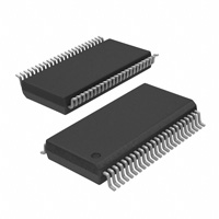


 工商网监
湘ICP备2023018690号
工商网监
湘ICP备2023018690号
