CY8C29466, CY8C29566 CY8C29666, CY8C29866
PSoC® Programmable System-on-Chip™
1. Features
■ ■
Powerful Harvard Architecture Processor ❐ M8C Processor Speeds to 24 MHz ❐ Two 8x8 Multiply, 32-Bit Accumulate ❐ Low Power at High Speed ❐ 3.0V to 5.25V Operating Voltage ❐ Operating Voltages Down to 1.0V Using On-Chip Switch Mode Pump (SMP) ❐ Industrial Temperature Range: -40°C to +85°C Advanced Peripherals (PSoC® Blocks) ❐ 12 Rail-to-Rail Analog PSoC Blocks Provide: • Up to 14-Bit ADCs • Up to 9-Bit DACs • Programmable Gain Amplifiers • Programmable Filters and Comparators ❐ 16 Digital PSoC Blocks Provide: • 8- to 32-Bit Timers, Counters, and PWMs • CRC and PRS Modules • Up to 4 Full-Duplex UARTs • Multiple SPI™ Masters or Slaves • Connectable to all GPIO Pins ❐ Complex Peripherals by Combining Blocks Precision, Programmable Clocking ❐ Internal ±2.5% 24/48 MHz Oscillator ❐ 24/48 MHz with Optional 32.768 kHz Crystal ❐ Optional External Oscillator, up to 24 MHz ❐ Internal Oscillator for Watchdog and Sleep Flexible On-Chip Memory ❐ 32K Bytes Flash Program Storage 50,000 Erase/Write Cycles ❐ 2K Bytes SRAM Data Storage ❐ In-System Serial Programming (ISSP) ❐ Partial Flash Updates ❐ Flexible Protection Modes ❐ EEPROM Emulation in Flash Programmable Pin Configurations ❐ 25 mA Sink, 10 mA Source on all GPIO ❐ Pull up, Pull down, High Z, Strong, or Open Drain Drive Modes on all GPIO ❐ 8 standard analog inputs on GPIO, plus 4 additional analog inputs with restricted routing ❐ Four 40 mA Analog Outputs on GPIO ❐ Configurable Interrupt on all GPIO
Additional System Resources ❐ I2C Slave, Master, and Multi-Master to 400 kHz ❐ Watchdog and Sleep Timers ❐ User-Configurable Low Voltage Detection ❐ Integrated Supervisory Circuit ❐ On-Chip Precision Voltage Reference Complete Development Tools ❐ Free Development Software (PSoC Designer™) ❐ Full-Featured, In-Circuit Emulator and Programmer ❐ Full Speed Emulation ❐ Complex Breakpoint Structure ❐ 128K Bytes Trace Memory ❐ Complex Events ❐ C Compilers, Assembler, and Linker
■
■
2. Logic Block Diagram
Port 5 Port 4 Port 3 Port 2 Port 1 Port 0
PSoC CORE
System Bus
Global Digital Interconnect SRAM 256 Bytes Interrupt Controller
Analog Drivers
■
Global Analog Interconnect Flash 16K Sleep and Watchdog
SROM
■
CPUCore (M8C)
Multiple Clock Sources (Includes IMO, ILO, PLL, and ECO)
DIGITAL SYSTEM
Digital Block Array
ANALOG SYSTEM
Analog Block Array
Analog Ref.
■
Analog Input Muxing
Digital Clocks
Multiply Accum.
POR and LVD Decimator I 2C System Resets
Internal Voltage Ref.
Switch Mode Pump
SYSTEM RESOURCES
Cypress Semiconductor Corporation Document Number: 38-12013 Rev. *K
•
198 Champion Court
•
San Jose, CA 95134-1709
• 408-943-2600 Revised April 20, 2009
[+] Feedback
�CY8C29466, CY8C29566 CY8C29666, CY8C29866
3. PSoC Functional Overview
The PSoC family consists of many Programmable System-on-Chip Controller devices. These devices are designed to replace multiple traditional MCU-based system components with one, low cost single-chip programmable device. PSoC devices include configurable blocks of analog and digital logic, as well as programmable interconnects. This architecture allows the user to create customized peripheral configurations that match the requirements of each individual application. Additionally, a fast CPU, Flash program memory, SRAM data memory, and configurable IO are included in a range of convenient pinouts and packages. The PSoC architecture, as illustrated on the left, is comprised of four main areas: PSoC Core, Digital System, Analog System, and System Resources. Configurable global busing allows all the device resources to be combined into a complete custom system. The PSoC CY8C29x66 family can have up to five IO ports that connect to the global digital and analog interconnects, providing access to 8 digital blocks and 12 analog blocks.
3.2 Digital System
The Digital System is composed of 8 digital PSoC blocks. Each block is an 8-bit resource that can be used alone or combined with other blocks to form 8, 16, 24, and 32-bit peripherals, which are called user module references. Figure 3-1. Digital System Block Diagram
Port 5 Port 4 Port 3 Port 2 Port 1 Port 0
Digital Clocks FromCore
To System Bus
ToAnalog System
DIGITAL SYSTEM
Digital PSoC Block Array
Row Input Configuration
Row 0
DBB00 DBB01 DCB02
4 DCB03 4
Row Output Configuration
3.1 PSoC Core
The PSoC Core is a powerful engine that supports a rich feature set. The core includes a CPU, memory, clocks, and configurable GPIO (General Purpose IO). The M8C CPU core is a powerful processor with speeds up to 24 MHz, providing a four MIPS 8-bit Harvard architecture microprocessor. The CPU uses an interrupt controller with 17 vectors, to simplify programming of real time embedded events. Program execution is timed and protected using the included Sleep and Watch Dog Timers (WDT). Memory encompasses 16K of Flash for program storage, 256 bytes of SRAM for data storage, and up to 2K of EEPROM emulated using the Flash. Program Flash utilizes four protection levels on blocks of 64 bytes, allowing customized software IP protection. The PSoC device incorporates flexible internal clock generators, including a 24 MHz IMO (internal main oscillator) accurate to 2.5% over temperature and voltage. The 24 MHz IMO can also be doubled to 48 MHz for use by the digital system. A low power 32 kHz ILO (internal low speed oscillator) is provided for the Sleep timer and WDT. If crystal accuracy is desired, the ECO (32.768 kHz external crystal oscillator) is available for use as a Real Time Clock (RTC) and can optionally generate a crystal-accurate 24 MHz system clock using a PLL. The clocks, together with programmable clock dividers (as a System Resource), provide the flexibility to integrate almost any timing requirement into the PSoC device. PSoC GPIOs provide connection to the CPU, digital and analog resources of the device. Each pin’s drive mode may be selected from eight options, allowing great flexibility in external interfacing. Every pin also has the capability to generate a system interrupt on high level, low level, and change from last read.
8 8
8
Row Input Configuration
Row 1
DBB10 DBB11 DCB12
4 DCB13 4
8 Row Output Configuration
GIE[7:0] GIO[7:0]
Global Digital Interconnect
GOE[7:0] GOO[7:0]
Digital peripheral configurations include those listed below.
■ ■ ■ ■ ■ ■ ■ ■ ■ ■
PWMs (8 to 32 bit) PWMs with Dead band (8 to 32 bit) Counters (8 to 32 bit) Timers (8 to 32 bit) UART 8 bit with selectable parity (up to 2) SPI slave and master (up to 2) I2C slave and multi-master (1 available as a System Resource) Cyclical Redundancy Checker/Generator (8 to 32 bit) IrDA (up to 2) Pseudo Random Sequence Generators (8 to 32 bit)
The digital blocks can be connected to any GPIO through a series of global buses that can route any signal to any pin. The buses also allow for signal multiplexing and for performing logic operations. This configurability frees your designs from the constraints of a fixed peripheral controller. Digital blocks are provided in rows of four, where the number of blocks varies by PSoC device family. This allows you the optimum choice of system resources for your application. Family resources are shown in the table titled “PSoC Device Characteristics” on page 4.
Document Number: 38-12013 Rev. *K
Page 2 of 46
[+] Feedback
�CY8C29466, CY8C29566 CY8C29666, CY8C29866
3.3 Analog System
The Analog System is composed of 12 configurable blocks, each comprised of an opamp circuit allowing the creation of complex analog signal flows. Analog peripherals are very flexible and can be customized to support specific application requirements. Some of the more common PSoC analog functions (most available as user modules) are listed below.
■ ■ ■ ■ ■ ■ ■ ■ ■ ■ ■ ■ ■ ■
Figure 3-2. Analog System Block Diagram
P0[7] P0[5] P0[3] P0[1] AGNDIn RefIn P0[6] P0[4] P0[2] P0[0] P2[6]
Analog-to-digital converters (up to 4, with 6- to 14-bit resolution, selectable as Incremental, Delta Sigma, and SAR) Filters (2, 4, 6, and 8 pole band-pass, low-pass, and notch) Amplifiers (up to 4, with selectable gain to 48x) Instrumentation amplifiers (up to 2, with selectable gain to 93x) Comparators (up to 4, with 16 selectable thresholds) DACs (up to 4, with 6- to 9-bit resolution) Multiplying DACs (up to 4, with 6- to 9-bit resolution) High current output drivers (four with 30 mA drive as a Core Resource) 1.3V reference (as a System Resource) DTMF Dialer Modulators Correlators Peak detectors Many other topologies possible
P2[3]
P2[4] P2[2] P2[0]
P2[1]
Array Input Configuration
ACI0[1:0]
ACI1[1:0]
ACI2[1:0]
ACI3[1:0]
Block Array
ACB00 ASC10 ASD20 ACB01 ASD11 ASC21 ACB02 ASC12 ASD22 ACB03 ASD13 ASC23
Analog blocks are provided in columns of three, which includes one CT (Continuous Time) and two SC (Switched Capacitor) blocks, as shown in the figure below.
Interface to Digital System RefHi RefLo AGND
Analog Reference
Reference Generators AGNDIn RefIn Bandgap
M8C Interface (Address Bus, Data Bus, Etc.)
3.4 Additional System Resources
System Resources, some of which have been previously listed, provide additional capability useful to complete systems. Additional resources include a multiplier, decimator, switch mode pump, low voltage detection, and power on reset. Statements describing the merits of each system resource are below. Digital clock dividers provide three customizable clock frequencies for use in applications. The clocks can be routed to both the digital and analog systems. Additional clocks can be generated using digital PSoC blocks as clock dividers. ■ Multiply accumulate (MAC) provides fast 8-bit multiplier with 32-bit accumulate, to assist in general math and digital filters. ■ The decimator provides a custom hardware filter for digital signal processing applications including the creation of Delta Sigma ADCs. ■ The I2C module provides 100 and 400 kHz communication over two wires. Slave, master, and multi-master modes are all supported.
■
Document Number: 38-12013 Rev. *K
Page 3 of 46
[+] Feedback
�CY8C29466, CY8C29566 CY8C29666, CY8C29866
■
■ ■
Low Voltage Detection (LVD) interrupts can signal the application of falling voltage levels, while the advanced POR (Power On Reset) circuit eliminates the need for a system supervisor. An internal 1.3V reference provides an absolute reference for the analog system, including ADCs and DACs. An integrated switch mode pump (SMP) generates normal operating voltages from a single 1.2V battery cell, providing a low cost boost converter.
4. Getting Started
The quickest way to understand PSoC silicon is to read this data sheet and then use the PSoC Designer Integrated Development Environment (IDE). This data sheet is an overview of the PSoC integrated circuit and presents specific pin, register, and electrical specifications. For in depth information, along with detailed programming details, see the PSoC® Programmable System-on-Chip™ Technical Reference Manual for CY8C28xxx PSoC devices. For up to date ordering, packaging, and electrical specification information, see the latest PSoC device data sheets on the web at www.cypress.com/psoc.
3.5 PSoC Device Characteristics
Depending on your PSoC device characteristics, the digital and analog systems can have 16, 8, or 4 digital blocks and 12, 6, or 4 analog blocks. The following table lists the resources available for specific PSoC device groups.The PSoC device covered by this data sheet is highlighted below. Table 3-1. PSoC Device Characteristics
Analog Columns Analog Outputs Analog Inputs Analog Blocks Digital Blocks Digital IO Digital Rows SRAM Size PSoC Part Number CY8C29x66 CY8C27x43 CY8C24x94 CY8C24x23 CY8C24x23A CY8C21x34 CY8C21x23 CY8C20x34 Flash Size
4.1 Application Notes
Application notes are an excellent introduction to the wide variety of possible PSoC designs. They are located here: www.cypress.com/psoc. Select Application Notes under the Documentation tab.
up to 64 up to 44 49 up to 24 up to 24 up to 28 16 up to 28
4 2 1 1 1 1 1 0
16 8 4 4 4 4 4 0
12 12 48 12 12 28 8 28
4 4 2 2 2 0 0 0
4 4 2 2 2 2 2 0
12 12 6 6 6 4[1] 4[1] 3[2]
2K 256 Bytes 1K 256 Bytes 256 Bytes 512 Bytes 256 Bytes 512 Bytes
32K 16K 16K 4K 4K 8K 4K 8K
4.2 Development Kits
PSoC Development Kits are available online from Cypress at www.cypress.com/shop and through a growing number of regional and global distributors, which include Arrow, Avnet, Digi-Key, Farnell, Future Electronics, and Newark.
4.3 Training
Free PSoC technical training (on demand, webinars, and workshops) is available online at www.cypress.com/training. The training covers a wide variety of topics and skill levels to assist you in your designs.
4.4 CYPros Consultants
Certified PSoC Consultants offer everything from technical assistance to completed PSoC designs. To contact or become a PSoC Consultant go to www.cypress.com/cypros.
4.5 Solutions Library
Visit our growing library of solution focused designs at www.cypress.com/solutions. Here you can find various application designs that include firmware and hardware design files that enable you to complete your designs quickly.
4.6 Technical Support
For assistance with technical issues, search KnowledgeBase articles and forums at www.cypress.com/support. If you cannot find an answer to your question, call technical support at 1-800-541-4736.
Notes 1. Limited analog functionality. 2. Two analog blocks and one CapSense.
Document Number: 38-12013 Rev. *K
Page 4 of 46
[+] Feedback
�CY8C29466, CY8C29566 CY8C29666, CY8C29866
5. Development Tools
PSoC Designer is a Microsoft® Windows-based, integrated development environment for the Programmable System-on-Chip (PSoC) devices. The PSoC Designer IDE runs on Windows XP or Windows Vista. This system provides design database management by project, an integrated debugger with In-Circuit Emulator, in-system programming support, and built in support for third party assemblers and C compilers. PSoC Designer also supports C language compilers developed specifically for the devices in the PSoC family. 5.1.4 Code Generation Tools PSoC Designer supports multiple third party C compilers and assemblers. The code generation tools work seamlessly within the PSoC Designer interface and have been tested with a full range of debugging tools. The choice is yours. Assemblers. The assemblers allow assembly code to merge seamlessly with C code. Link libraries automatically use absolute addressing or are compiled in relative mode, and linked with other software modules to get absolute addressing. C Language Compilers. C language compilers are available that support the PSoC family of devices. The products allow you to create complete C programs for the PSoC family devices. The optimizing C compilers provide all the features of C tailored to the PSoC architecture. They come complete with embedded libraries providing port and bus operations, standard keypad and display support, and extended math functionality. 5.1.5 Debugger The PSoC Designer Debugger subsystem provides hardware in-circuit emulation, allowing you to test the program in a physical system while providing an internal view of the PSoC device. Debugger commands allow the designer to read and program and read and write data memory, read and write IO registers, read and write CPU registers, set and clear breakpoints, and provide program run, halt, and step control. The debugger also allows the designer to create a trace buffer of registers and memory locations of interest. 5.1.6 Online Help System The online help system displays online, context-sensitive help for the user. Designed for procedural and quick reference, each functional subsystem has its own context-sensitive help. This system also provides tutorials and links to FAQs and an Online Support Forum to aid the designer in getting started.
5.1 PSoC Designer Software Subsystems
5.1.1 System-Level View A drag-and-drop visual embedded system design environment based on PSoC Express. In the system level view you create a model of your system inputs, outputs, and communication interfaces. You define when and how an output device changes state based upon any or all other system devices. Based upon the design, PSoC Designer automatically selects one or more PSoC Programmable System-on-Chip Controllers that match your system requirements. PSoC Designer generates all embedded code, then compiles and links it into a programming file for a specific PSoC device. 5.1.2 Chip-Level View The chip-level view is a more traditional integrated development environment (IDE) based on PSoC Designer 4.4. Choose a base device to work with and then select different onboard analog and digital components called user modules that use the PSoC blocks. Examples of user modules are ADCs, DACs, Amplifiers, and Filters. Configure the user modules for your chosen application and connect them to each other and to the proper pins. Then generate your project. This prepopulates your project with APIs and libraries that you can use to program your application. The device editor also supports easy development of multiple configurations and dynamic reconfiguration. Dynamic configuration allows for changing configurations at run time. 5.1.3 Hybrid Designs You can begin in the system-level view, allow it to choose and configure your user modules, routing, and generate code, then switch to the chip-level view to gain complete control over on-chip resources. All views of the project share a common code editor, builder, and common debug, emulation, and programming tools.
5.2 In-Circuit Emulator
A low cost, high functionality In-Circuit Emulator (ICE) is available for development support. This hardware has the capability to program single devices. The emulator consists of a base unit that connects to the PC by way of a USB port. The base unit is universal and operates with all PSoC devices. Emulation pods for each device family are available separately. The emulation pod takes the place of the PSoC device in the target board and performs full speed (24 MHz) operation.
Document Number: 38-12013 Rev. *K
Page 5 of 46
[+] Feedback
�CY8C29466, CY8C29566 CY8C29666, CY8C29866
6. Designing with PSoC Designer
The development process for the PSoC device differs from that of a traditional fixed function microprocessor. The configurable analog and digital hardware blocks give the PSoC architecture a unique flexibility that pays dividends in managing specification change during development and by lowering inventory costs. These configurable resources, called PSoC Blocks, have the ability to implement a wide variety of user selectable functions. The PSoC development process can be summarized in the following four steps: 1. Select Components 2. Configure Components 3. Organize and Connect 4. Generate, Verify, and Debug
6.3 Organize and Connect
You can build signal chains at the chip level by interconnecting user modules to each other and the IO pins, or connect system level inputs, outputs, and communication interfaces to each other with valuator functions. In the system-level view, selecting a potentiometer driver to control a variable speed fan driver and setting up the valuators to control the fan speed based on input from the pot selects, places, routes, and configures a programmable gain amplifier (PGA) to buffer the input from the potentiometer, an analog to digital converter (ADC) to convert the potentiometer’s output to a digital signal, and a PWM to control the fan. In the chip-level view, perform the selection, configuration, and routing so that you have complete control over the use of all on-chip resources.
6.1 Select Components
Both the system-level and chip-level views provide a library of prebuilt, pretested hardware peripheral components. In the system-level view, these components are called “drivers” and correspond to inputs (a thermistor, for example), outputs (a brushless DC fan, for example), communication interfaces (I2C-bus, for example), and the logic to control how they interact with one another (called valuators). In the chip-level view, the components are called “user modules”. User modules make selecting and implementing peripheral devices simple, and come in analog, digital, and programmable system-on-chip varieties.
6.4 Generate, Verify, and Debug
When you are ready to test the hardware configuration or move on to developing code for the project, perform the “Generate Application” step. This causes PSoC Designer to generate source code that automatically configures the device to your specification and provides the software for the system. Both system-level and chip-level designs generate software based on your design. The chip-level design provides application programming interfaces (APIs) with high level functions to control and respond to hardware events at run time and interrupt service routines that you can adapt as needed. The system-level design also generates a C main() program that completely controls the chosen application and contains placeholders for custom code at strategic positions allowing you to further refine the software without disrupting the generated code. A complete code development environment allows you to develop and customize your applications in C, assembly language, or both. The last step in the development process takes place inside the PSoC Designer’s Debugger subsystem. The Debugger downloads the HEX image to the ICE where it runs at full speed. Debugger capabilities rival those of systems costing many times more. In addition to traditional single-step, run-to-breakpoint and watch-variable features, the Debugger provides a large trace buffer and allows you define complex breakpoint events that include monitoring address and data bus values, memory locations and external signals.
6.2 Configure Components
Each of the components you select establishes the basic register settings that implement the selected function. They also provide parameters and properties that allow you to tailor their precise configuration to your particular application. For example, a Pulse Width Modulator (PWM) User Module configures one or more digital PSoC blocks, one for each 8 bits of resolution. The user module parameters permit you to establish the pulse width and duty cycle. Configure the parameters and properties to correspond to your chosen application. Enter values directly or by selecting values from drop-down menus. Both the system-level drivers and chip-level user modules are documented in data sheets that are viewed directly in the PSoC Designer. These data sheets explain the internal operation of the component and provide performance specifications. Each data sheet describes the use of each user module parameter or driver property, and other information you may need to successfully implement your design.
Document Number: 38-12013 Rev. *K
Page 6 of 46
[+] Feedback
�CY8C29466, CY8C29566 CY8C29666, CY8C29866
7. Document Conventions
7.1 Acronyms Used
This table lists the acronyms used in this data sheet. Table 7-1. Acronyms Acronym AC ADC API CPU CT DAC DC EEPROM FSR GPIO ICE IDE IO ISSP IPOR LSb LVD MSb PC PGA POR PPOR PSoC® PWM ROM SC SMP SRAM Description alternating current analog-to-digital converter application programming interface central processing unit continuous time digital-to-analog converter direct current electrically erasable programmable read-only memory full scale range general purpose IO in-circuit emulator integrated development environment input/output in-system serial programming imprecise power on reset least-significant bit low voltage detect most-significant bit program counter programmable gain amplifier power on reset precision power on reset Programmable System-on-Chip™ pulse width modulator read only memory switched capacitor switch mode pump static random access memory
7.2 Units of Measure
A units of measure table is located in the section Electrical Specifications on page 19. Table 11-1 on page 19 lists all the abbreviations used to measure the PSoC devices.
7.3 Numeric Naming
Hexadecimal numbers are represented with all letters in uppercase with an appended lowercase ‘h’ (for example, ‘14h’ or ‘3Ah’). Hexadecimal numbers may also be represented by a ‘0x’ prefix, the C coding convention. Binary numbers have an appended lowercase ‘b’ (for example, 01010100b’ or ‘01000011b’). Numbers not indicated by an ‘h’, ‘b’, or 0x are decimal.
Document Number: 38-12013 Rev. *K
Page 7 of 46
[+] Feedback
�CY8C29466, CY8C29566 CY8C29666, CY8C29866
8. Pinouts
The CY8C29x66 PSoC device is available in a variety of packages which are listed and illustrated in the following tables. Every port pin (labeled with a “P”) is capable of Digital IO. However, Vss, Vdd, SMP, and XRES are not capable of Digital IO.
8.1 28-Pin Part Pinout
Table 8-1. 28-Pin Part Pinout (PDIP, SSOP, SOIC)
Pin No. 1 2 3 4 5 6 7 8 9 10 11 12 13 14 15 16 17 18 19 20 21 22 23 24 25 26 27 28 Type Digital Analog IO I IO IO IO IO IO I IO IO IO I IO I Power IO IO IO IO Power IO IO IO IO Input IO IO IO IO IO IO IO IO Power I I Pin Name P0[7] P0[5] P0[3] P0[1] P2[7] P2[5] P2[3] P2[1] SMP P1[7] P1[5] P1[3] P1[1] Vss P1[0] P1[2] P1[4] P1[6] XRES P2[0] P2[2] P2[4] P2[6] P0[0] P0[2] P0[4] P0[6] Vdd Description Analog column mux input. Analog column mux input and column output. Analog column mux input and column output. Analog column mux input.
Figure 8-1. CY8C29466 28-Pin PSoC Device
A, I, P0[7] A, IO, P0[5] A, IO, P0[3] A, I, P0[1] P2[7] P2[5] A, I, P2[3] A, I, P2[1] SMP I2CSCL,P1[7] I2CSDA, P1[5] P1[3] I2CSCL,XTALin, P1[1] Vss
Direct switched capacitor block input. Direct switched capacitor block input. Switch Mode Pump (SMP) connection to external components required. I2C Serial Clock (SCL). I2C Serial Data (SDA). Crystal (XTALin), I2C Serial Clock (SCL), ISSP-SCLK*. Ground connection. Crystal (XTALout), I2C Serial Data (SDA), ISSP-SDATA*. Optional External Clock Input (EXTCLK). Active high external reset with internal pull down. Direct switched capacitor block input. Direct switched capacitor block input. External Analog Ground (AGND). External Voltage Reference (VREF). Analog column mux input. Analog column mux input and column output. Analog column mux input and column output. Analog column mux input. Supply voltage.
1 2 3 4 5 6 7 8 9 10 11 12 13 14
PDIP SSOP SOIC
28 27 26 25 24 23 22 21 20 19 18 17 16 15
Vdd P0[6], A, I P0[4], A, IO P0[2], A, IO P0[0], A, I P2[6],ExternalVREF P2[4],ExternalAGND P2[2], A, I P2[0], A, I XRES P1[6] P1[4],EXTCLK P1[2] P1[0],XTALout,I2CSDA
I IO IO I
LEGEND: A = Analog, I = Input, and O = Output. * These are the ISSP pins, which are not High Z at POR (Power On Reset). See the PSoC Programmable System-on-Chip Technical Reference Manual for details.
Document Number: 38-12013 Rev. *K
Page 8 of 46
[+] Feedback
�CY8C29466, CY8C29566 CY8C29666, CY8C29866
8.2 44-Pin Part Pinout
Table 8-2. 44-Pin Part Pinout (TQFP)
Pin No. 1 2 3 4 5 6 7 8 9 10 11 12 13 14 15 16 17 18 19 20 21 22 23 24 25 26 27 28 29 30 31 32 33 34 35 36 37 38 39 40 41 42 43 44 Type Digital Analog IO IO I IO I IO IO IO IO Power IO IO IO IO IO IO IO IO Power IO IO IO IO IO IO IO IO Input IO IO IO IO IO IO IO IO IO IO IO IO Power IO IO IO IO IO I IO IO I Pin Name P2[5] P2[3] P2[1] P4[7] P4[5] P4[3] P4[1] SMP P3[7] P3[5] P3[3] P3[1] P1[7] P1[5] P1[3] P1[1] Vss P1[0] P1[2] P1[4] P1[6] P3[0] P3[2] P3[4] P3[6] XRES P4[0] P4[2] P4[4] P4[6] P2[0] P2[2] P2[4] P2[6] P0[0] P0[2] P0[4] P0[6] Vdd P0[7] P0[5] P0[3] P0[1] P2[7] Description Direct switched capacitor block input. Direct switched capacitor block input.
Figure 8-2. CY8C29566 44-Pin PSoC Device
P0[6], A, I P0[4], A, IO P0[2], A, IO P0[0], A, I P2[6],ExternalVREF 33 32 31 30 29 28 27 26 25 24 23 P2[4],External AGND P2[2], A, I P2[0], A, I P4[6] P4[4] P4[2] P4[0] XRES P3[6] P3[4] P3[2]
Switch Mode Pump (SMP) connection to external components required.
I2C Serial Clock (SCL). I2C Serial Data (SDA). Crystal (XTALin), I2C Serial Clock (SCL), ISSP-SCLK*. Ground connection. Crystal (XTALout), I2C Serial Data (SDA), ISSP-SDATA*. Optional External Clock Input (EXTCLK).
Active high external reset with internal pull down.
I I
I IO IO I
Direct switched capacitor block input. Direct switched capacitor block input. External Analog Ground (AGND). External Voltage Reference (VREF). Analog column mux input. Analog column mux input and column output. Analog column mux input and column output. Analog column mux input. Supply voltage. Analog column mux input. Analog column mux input and column output. Analog column mux input and column output. Analog column mux input.
LEGEND: A = Analog, I = Input, and O = Output. * These are the ISSP pins, which are not High Z at POR (Power On Reset). See the PSoC Programmable System-on-ChipTechnical Reference Manual for details.
Document Number: 38-12013 Rev. *K
P3[1] I2CSCL, P1[7] I2C SDA, P1[5] P1[3] I2CSCL,XTALin,P1[1] Vss I2CSDA,XTALout,P1[0] P1[2] EXTCLK,P1[4] P1[6] P3[0]
12 13 14 15 16 17 18 19 20 21 22
P2[5] A, I, P2[3] A, I, P2[1] P4[7] P4[5] P4[3] P4[1] SMP P3[7] P3[5] P3[3]
1 2 3 4 5 6 7 8 9 10 11
44 43 42 41 40 39 38 37 36 35 34
P2[7] P0[1], A, I P0[3], A, IO P0[5], A, IO P0[7], A, I Vdd
TQFP
Page 9 of 46
[+] Feedback
�CY8C29466, CY8C29566 CY8C29666, CY8C29866
8.3 48-Pin Part Pinouts
Table 8-3. 48-Pin Part Pinout (SSOP)
Pin No. 1 2 3 4 5 6 7 8 9 10 11 12 13 14 15 16 17 18 19 20 21 22 23 24 25 26 27 28 29 30 31 32 33 34 35 36 37 38 39 40 41 42 43 44 45 46 47 48 Type Digital Analog IO I IO IO IO IO IO I IO IO IO I IO I IO IO IO IO Power IO IO IO IO IO IO IO IO IO IO Power IO IO IO IO IO IO IO IO IO IO Input IO IO IO IO IO IO IO IO IO IO IO IO Power Pin Name P0[7] P0[5] P0[3] P0[1] P2[7] P2[5] P2[3] P2[1] P4[7] P4[5] P4[3] P4[1] SMP P3[7] P3[5] P3[3] P3[1] P5[3] P5[1] P1[7] P1[5] P1[3] P1[1] Vss P1[0] P1[2] P1[4] P1[6] P5[0] P5[2] P3[0] P3[2] P3[4] P3[6] XRES P4[0] P4[2] P4[4] P4[6] P2[0] P2[2] P2[4] P2[6] P0[0] P0[2] P0[4] P0[6] Vdd Description Analog column mux input. Analog column mux input and column output. Analog column mux input and column output. Analog column mux input.
Figure 8-3. CY8C29666 48-Pin PSoC Device
A, I, P0[7] A, IO, P0[5] A, IO, P0[3] A, I, P0[1] P2[7] P2[5] A, I, P2[3] A, I, P2[1] P4[7] P4[5] P4[3] P4[1] SMP P3[7] P3[5] P3[3] P3[1] P5[3] P5[1] I2CSCL, P1[7] I2CSDA, P1[5] P1[3] I2CSCL,XTALin,P1[1] Vss 1 2 3 4 5 6 7 8 9 10 11 12 13 14 15 16 17 18 19 20 21 22 23 24
Direct switched capacitor block input. Direct switched capacitor block input.
Switch Mode Pump (SMP) connection to external components required.
SSOP
I2C Serial Clock (SCL). I2C Serial Data (SDA). Crystal (XTALin), I2C Serial Clock (SCL), ISSP-SCLK*. Ground connection. Crystal (XTALout), I2C Serial Data (SDA), ISSP-SDATA*. Optional External Clock Input (EXTCLK).
48 47 46 45 44 43 42 41 40 39 38 37 36 35 34 33 32 31 30 29 28 27 26 25
Vdd P0[6], A, I P0[4], A, IO P0[2], A, IO P0[0], A, I P2[6],External VREF P2[4],External AGND P2[2], A, I P2[0], A, I P4[6] P4[4] P4[2] P4[0] XRES P3[6] P3[4] P3[2] P3[0] P5[2] P5[0] P1[6] P1[4],EXTCLK P1[2] P1[0],XTALout,I2C SDA
Active high external reset with internal pull down.
I I
I IO IO I
Direct switched capacitor block input. Direct switched capacitor block input. External Analog Ground (AGND). External Voltage Reference (VREF). Analog column mux input. Analog column mux input and column output. Analog column mux input and column output. Analog column mux input. Supply voltage.
LEGEND: A = Analog, I = Input, and O = Output. * These are the ISSP pins, which are not High Z at POR (Power On Reset). See the PSoC Programmable System-on-Chip Technical Reference Manual for details.
Document Number: 38-12013 Rev. *K
Page 10 of 46
[+] Feedback
�CY8C29466, CY8C29566 CY8C29666, CY8C29866
Table 8-4. 48-Pin Part Pinout (QFN)**
Pin No. 1 2 3 4 5 6 7 8 9 10 11 12 13 14 15 16 17 18 19 20 21 22 23 24 25 26 27 28 29 30 31 32 33 34 35 36 37 38 39 40 41 42 43 44 45 46 47 48 IO IO IO IO IO IO IO IO IO IO IO IO IO IO IO IO IO IO Power I IO IO I I IO IO I I I IO IO IO IO IO IO IO IO IO IO Input IO IO IO IO IO IO IO IO IO IO Power Type Digital IO IO IO IO IO IO Power Analog I I Pin Name P2[3] P2[1] P4[7] P4[5] P4[3] P4[1] SMP P3[7] P3[5] P3[3] P3[1] P5[3] P5[1] P1[7] P1[5] P1[3] P1[1] Vss P1[0] P1[2] P1[4] P1[6] P5[0] P5[2] P3[0] P3[2] P3[4] P3[6] XRES P4[0] P4[2] P4[4] P4[6] P2[0] P2[2] P2[4] P2[6] P0[0] P0[2] P0[4] P0[6] Vdd P0[7] P0[5] P0[3] P0[1] P2[7] P2[5] Direct switched capacitor block input. Direct switched capacitor block input. External Analog Ground (AGND). External Voltage Reference (VREF). Analog column mux input. Analog column mux input and column output. Analog column mux input and column output. Analog column mux input. Supply voltage. Analog column mux input. Analog column mux input and column output. Analog column mux input and column output. Analog column mux input. Active high external reset with internal pull down. Optional External Clock Input (EXTCLK). Crystal (XTALin), I2C Serial Clock (SCL), ISSP-SCLK*. Ground connection. Crystal (XTALout), I2C Serial Data (SDA), ISSP-SDATA*. I2C Serial Clock (SCL). I2C Serial Data (SDA). Switch Mode Pump (SMP) connection to external components required. Description Direct switched capacitor block input. Direct switched capacitor block input.
Figure 8-4. CY8C29666 48-Pin PSoC Device
Vdd P0[6], A,I P0[4], A,IO P0[2], A,IO P0[0], A,I P2[6],ExternalVREF 36 35 34 33 32 31 30 29 28 27 26 25 P2[4],External AGND P2[2], A, I P2[0], A, I P4[6] P4[4] P4[2] P4[0] XRES P3[6] P3[4] P3[2] P3[0] 42 41 40 39 38 37
LEGEND: A = Analog, I = Input, and O = Output. * These are the ISSP pins, which are not High Z at POR (Power On Reset). See the PSoC Programmable System-on-Chip Technical Reference Manual for details. ** The QFN package has a center pad that must be connected to ground (Vss).
Document Number: 38-12013 Rev. *K
13 14 I2CSDA,P1[5] 15 P1[3] 16 I2CSCL,XTALin,P1[1] 17 Vss 18 I2CSDA,XTALout,P1[0] 19 P1[2] 20 EXTCLK,P1[4] 21 P1[6] 22 P5[0] 23 P5[2] 24
A, I, P2[3] A, I, P2[1] P4[7] P4[5] P4[3] P4[1] SMP P3[7] P3[5] P3[3] P3[1] P5[3]
1 2 3 4 5 6 7 8 9 10 11 12
P5[1] I2CSCL,P1[7]
48 47 46 45 44 43
P2[5] P2[7] P0[1], A,I P0[3], A,IO P0[5], A,IO P0[7], A,I
QFN
(Top View )
Page 11 of 46
[+] Feedback
�CY8C29466, CY8C29566 CY8C29666, CY8C29866
8.4 100-Pin Part Pinout
Table 8-5. 100-Pin Part Pinout (TQFP)
Pin No. 1 2 3 4 5 6 7 8 9 10 11 12 13 14 15 16 17 18 19 20 21 22 23 24 25 26 27 28 29 30 31 32 33 34 35 36 37 38 39 40 41 42 43 44 45 46 47 48 49 50 Type Digital Analog Name NC NC P0[1] P2[7] P2[5] P2[3] P2[1] P4[7] P4[5] P4[3] P4[1] NC NC SMP Vss P3[7] P3[5] P3[3] P3[1] P5[7] P5[5] P5[3] P5[1] P1[7] NC NC NC P1[5] P1[3] P1[1] NC Vdd NC Vss NC P7[7] P7[6] P7[5] P7[4] P7[3] P7[2] P7[1] P7[0] P1[0] P1[2] P1[4] P1[6] NC NC NC Description No connection. No connection. Analog column mux input. Pin No. 51 52 53 54 55 56 57 58 59 60 61 62 63 64 65 66 67 68 69 70 71 72 73 74 75 76 77 78 79 80 81 82 83 84 85 86 87 88 89 90 91 92 93 94 95 96 97 98 99 100 Type Digital Analog IO IO IO IO IO IO IO IO Name NC P5[0] P5[2] P5[4] P5[6] P3[0] P3[2] P3[4] P3[6] NC NC XRES P4[0] P4[2] Power IO IO IO IO IO IO IO I Vss P4[4] P4[6] P2[0] P2[2] P2[4] NC P2[6] NC P0[0] NC NC P0[2] NC P0[4] NC P0[6] Vdd Vdd Vss Vss P6[0] P6[1] P6[2] P6[3] P6[4] P6[5] P6[6] P6[7] NC P0[7] NC P0[5] NC P0[3] NC Ground connection. No connection. Description
IO IO IO IO IO IO IO IO IO
I
I I
Direct switched capacitor block input. Direct switched capacitor block input.
No connection. No connection. Switch Mode Pump (SMP) connection to external components required. Ground connection.
Input IO IO
No connection. No connection. Active high external reset with internal pull down.
Power Power IO IO IO IO IO IO IO IO IO
I I
IO IO IO
I2C Serial Clock (SCL). No connection. No connection. No connection. I2C Serial Data (SDA). Crystal (XTALin), I2C Serial Clock (SCL), ISSP-SCLK*. No connection. Supply voltage. No connection. Ground connection. No connection.
IO IO
IO IO
Direct switched capacitor block input. Direct switched capacitor block input. External Analog Ground (AGND). No connection. External Voltage Reference (VREF). No connection. Analog column mux input. No connection. No connection. Analog column mux input and column output. No connection. Analog column mux input and column output. No connection. Analog column mux input. Supply voltage. Supply voltage. Ground connection. Ground connection.
IO Power Power Power Power IO IO IO IO IO IO IO IO
I
Power Power IO IO IO IO IO IO IO IO IO IO IO IO
Crystal (XTALout), I2C Serial Data (SDA), ISSP-SDATA*. Optional External Clock Input (EXTCLK). No connection. No connection. No connection.
No connection. Analog column mux input. No connection. Analog column mux input and column output. No connection. Analog column mux input and column output. No connection.
IO IO IO
I IO IO
LEGEND: A = Analog, I = Input, and O = Output. * These are the ISSP pins, which are not High Z at POR (Power On Reset). See the PSoC Programmable System-on-Chip Technical Reference Manual for details.
Document Number: 38-12013 Rev. *K
Page 12 of 46
[+] Feedback
�CY8C29466, CY8C29566 CY8C29666, CY8C29866
Figure 8-5. CY8C29866 100-Pin PSoC Device
NC P0[3], A, IO NC P0[5], A, IO NC P0[7], A, I NC Vdd Vdd P0[6], A, I NC P0[4], A, IO NC P0[2], A, IO NC 77 76 75 74 73 72 71 70 69 68 67 66 65 64 63 62 61 60 59 58 57 56 55 54 53 52 51 NC P0[0], A, I NC P2[6],External VREF NC P2[4],External AGND P2[2], A, I P2[0], A, I P4[6] P4[4] Vss P4[2] P4[0] XRES NC NC P3[6] P3[4] P3[2] P3[0] P5[6] P5[4] P5[2] P5[0] NC
Document Number: 38-12013 Rev. *K
NC NC I2C SDA, P1[5] P1[3] XTALin,I2CSCL,P1[1] NC Vdd NC Vss NC P7[7] P7[6] P7[5] P7[4] P7[3] P7[2] P7[1] P7[0] XTALout,I2CSDA,P1[0] P1[2] EXTCLK,P1[4] P1[6] NC NC NC
26 27 28 29 30 31 32 33 34 35 36 37 38 39 40 41 42 43 44 45 46 47 48 49 50
NC NC A, I, P0[1] P2[7] P2[5] A, I, P2[3] A, I, P2[1] P4[7] P4[5] P4[3] P4[1] NC NC SMP Vss P3[7] P3[5] P3[3] P3[1] P5[7] P5[5] P5[3] P5[1] I2C SCL, P1[7] NC
1 2 3 4 5 6 7 8 9 10 11 12 13 14 15 16 17 18 19 20 21 22 23 24 25
100 99 98 97 96 95 94 93 92 91 90 89 88 87 86 85 84 83 82 81 80 79 78
P6[7] P6[6] P6[5] P6[4] P6[3] P6[2] P6[1] P6[0] Vss Vss
TQFP
Page 13 of 46
[+] Feedback
�CY8C29466, CY8C29566 CY8C29666, CY8C29866
8.5 100-Pin Part Pinout (On-Chip Debug)
The 100-pin TQFP part is for the CY8C29000 On-Chip Debug (OCD) PSoC device. Note OCD parts are only used for in-circuit debugging. OCD parts are NOT available for production Table 8-6. 100-Pin OCD Part Pinout (TQFP)
Analog Pin No. 1 2 3 4 5 6 7 8 9 10 11 12 13 14 15 16 17 18 19 20 21 22 23 24 25 26 27 28 29 30 31 32 33 34 35 36 37 38 39 40 41 42 43 44 Name NC NC P0[1] P2[7] P2[5] P2[3] P2[1] P4[7] P4[5] P4[3] P4[1] OCDE OCDO SMP Vss P3[7] P3[5] P3[3] P3[1] P5[7] P5[5] P5[3] P5[1] P1[7] NC NC NC P1[5] P1[3] P1[1]* NC Vdd NC Vss NC P7[7] P7[6] P7[5] P7[4] P7[3] P7[2] P7[1] P7[0] P1[0]* Description No internal connection. No internal connection. Analog column mux input. Pin No. 51 52 53 54 55 56 57 58 59 60 61 62 63 64 65 66 67 68 69 70 71 72 73 74 75 76 77 78 79 80 Analog Digital Digital Name NC P5[0] P5[2] P5[4] P5[6] P3[0] P3[2] P3[4] P3[6] HCLK CCLK XRES P4[0] P4[2] Vss P4[4] P4[6] P2[0] P2[2] P2[4] NC P2[6] NC P0[0] NC NC P0[2] NC P0[4] NC P0[6] Vdd Vdd Vss Vss P6[0] P6[1] P6[2] P6[3] P6[4] P6[5] P6[6] P6[7] NC P0[7] NC P0[5] NC P0[3] NC Description No internal connection.
IO IO IO IO IO IO IO IO IO
I
I I
Direct switched capacitor block input. Direct switched capacitor block input.
IO IO IO IO IO IO IO IO
Power Power IO IO IO IO IO IO IO IO IO
OCD even data IO OCD odd data output Switch Mode Pump (SMP) connection to required external components. Ground connection.
Input IO IO Power IO IO IO I IO I IO IO IO I
OCD high speed clock output OCD CPU clock output Active high pin reset with internal pull down.
Ground connection.
IO IO IO
I2C Serial Clock (SCL) No internal connection. No internal connection. No internal connection. I2C Serial Data (SDA). IFMTEST Crystal (XTALin), I2C Serial Clock (SCL), TC SCLK. No internal connection. Supply voltage. No internal connection. Ground connection. No internal connection.
IO IO
IO IO
Direct switched capacitor block input. Direct switched capacitor block input. External Analog Ground (AGND) input. No internal connection. External Voltage Reference (VREF) input. No internal connection. Analog column mux input. No internal connection. No internal connection. Analog column mux input and column output. No internal connection. Analog column mux input and column output, VREF. No internal connection. Analog column mux input. Supply voltage. Supply voltage. Ground connection. Ground connection.
81 IO I 82 Power 83 Power Power 84 Power 85 Power IO 86 IO IO 87 IO IO 88 IO IO 89 IO IO 90 IO IO 91 IO IO 92 IO IO 93 IO IO Crystal (XTALout), I2C Serial Data (SDA), TC 94 SDATA 45 IO P1[2] VFMTEST 95 IO I 46 IO P1[4] Optional External Clock Input (EXTCLK) 96 47 IO P1[6] 97 IO IO 48 NC No internal connection. 98 49 NC No internal connection. 99 IO IO 50 NC No internal connection. 100 LEGEND A = Analog, I = Input, O = Output, NC = No Connection, TC/TM: Test. * ISSP pin which is not HiZ at POR. Power
No internal connection. Analog column mux input. No internal connection. Analog column mux input and column output. No internal connection. Analog column mux input and column output. No internal connection.
Document Number: 38-12013 Rev. *K
Page 14 of 46
[+] Feedback
�CY8C29466, CY8C29566 CY8C29666, CY8C29866
Figure 8-6. CY8C29000 OCD (Not for Production)
NC P0[3], AIO NC P0[5], AIO NC P0[7], AI NC Vdd Vdd P0[6], AI NC P0[4], AIO NC P0[2], AIO NC 77 76 NC NC 75 74 73 72 71 70 69 68 67 66 65 64 63 62 61 60 59 58 57 56 55 54 53 52 51 NC P0[0], AI NC P2[6], External VREF NC P2[4], External AGND P2[2], AI P2[0], AI P4[6] P4[4] Vss P4[2] P4[0] XRES CCLK HCLK P3[6] P3[4] P3[2] P3[0] P5[6] P5[4] P5[2] P5[0] NC
100 99
98 97 96 95 94 93 92 91
90 89 88
26 27 28 29 30 31 32 33 34 35
NC NC I2C SDA, P1[5] P1[3] XTALin, I2C SCL, P1[1] NC Vdd NC Vss NC
Document Number: 38-12013 Rev. *K
P7[7] P7[6] P7[5] P7[4] P7[3] P7[2] P7[1] P7[0] XTALout, I2C SDA, P1[0] P1[2] EXTCLK, P1[4] P1[6] NC
36 37 38 39 40 41 42 43 44 45 46 47 48 49 50
NC NC AI, P0[1] P2[7] P2[5] AI, P2[3] AI, P2[1] P4[7] P4[5] P4[3] P4[1] OCDE OCDO SMP Vss P3[7] P3[5] P3[3] P3[1] P5[7] P5[5] P5[3] P5[1] I2C SCL, P1[7] NC
1 2 3 4 5 6 7 8 9 10 11 12 13 14 15 16 17 18 19 20 21 22 23 24 25
OCD TQFP
87 86 85 84 83 82 81 80 79 78
P6[7] P6[6] P6[5] P6[4] P6[3] P6[2] P6[1] P6[0] Vss Vss
Page 15 of 46
[+] Feedback
�CY8C29466, CY8C29566 CY8C29666, CY8C29866
This section lists the registers of the CY8C29x66 PSoC device. For detailed register information, reference the PSoC Programmable System-on-Chip Technical Reference Manual.
9. Register Conventions
9.1 Abbreviations Used
The register conventions specific to this section are listed in the following table. Convention R W L C # Description Read register or bit(s) Write register or bit(s) Logical register or bit(s) Clearable register or bit(s) Access is bit specific
10. Register Mapping Tables
The PSoC device has a total register address space of 512 bytes. The register space is referred to as IO space and is divided into two banks. The XOI bit in the Flag register (CPU_F) determines which bank the user is currently in. When the XOI bit is set the user is in Bank 1. Note In the following register mapping tables, blank fields are reserved and should not be accessed.
Document Number: 38-12013 Rev. *K
Page 16 of 46
[+] Feedback
�CY8C29466, CY8C29566 CY8C29666, CY8C29866
Table 10-1. Register Map Bank 0 Table: User Space
Name PRT0DR PRT0IE PRT0GS PRT0DM2 PRT1DR PRT1IE PRT1GS PRT1DM2 PRT2DR PRT2IE PRT2GS PRT2DM2 PRT3DR PRT3IE PRT3GS PRT3DM2 PRT4DR PRT4IE PRT4GS PRT4DM2 PRT5DR PRT5IE PRT5GS PRT5DM2 PRT6DR PRT6IE PRT6GS PRT6DM2 PRT7DR PRT7IE PRT7GS PRT7DM2 DBB00DR0 DBB00DR1 DBB00DR2 DBB00CR0 DBB01DR0 DBB01DR1 DBB01DR2 DBB01CR0 DCB02DR0 DCB02DR1 DCB02DR2 DCB02CR0 DCB03DR0 DCB03DR1 DCB03DR2 DCB03CR0 DBB10DR0 DBB10DR1 DBB10DR2 DBB10CR0 DBB11DR0 DBB11DR1 DBB11DR2 DBB11CR0 DCB12DR0 DCB12DR1 DCB12DR2 DCB12CR0 DCB13DR0 DCB13DR1 DCB13DR2 DCB13CR0 Addr (0,Hex) 00 01 02 03 04 05 06 07 08 09 0A 0B 0C 0D 0E 0F 10 11 12 13 14 15 16 17 18 19 1A 1B 1C 1D 1E 1F 20 21 22 23 24 25 26 27 28 29 2A 2B 2C 2D 2E 2F 30 31 32 33 34 35 36 37 38 39 3A 3B 3C 3D 3E 3F Access RW RW RW RW RW RW RW RW RW RW RW RW RW RW RW RW RW RW RW RW RW RW RW RW RW RW RW RW RW RW RW RW # W RW # # W RW # # W RW # # W RW # # W RW # # W RW # # W RW # # W RW # Name DBB20DR0 DBB20DR1 DBB20DR2 DBB20CR0 DBB21DR0 DBB21DR1 DBB21DR2 DBB21CR0 DCB22DR0 DCB22DR1 DCB22DR2 DCB22CR0 DCB23DR0 DCB23DR1 DCB23DR2 DCB23CR0 DBB30DR0 DBB30DR1 DBB30DR2 DBB30CR0 DBB31DR0 DBB31DR1 DBB31DR2 DBB31CR0 DCB32DR0 DCB32DR1 DCB32DR2 DCB32CR0 DCB33DR0 DCB33DR1 DCB33DR2 DCB33CR0 AMX_IN Addr (0,Hex) 40 41 42 43 44 45 46 47 48 49 4A 4B 4C 4D 4E 4F 50 51 52 53 54 55 56 57 58 59 5A 5B 5C 5D 5E 5F 60 61 62 63 64 65 66 67 68 69 6A 6B 6C 6D 6E 6F 70 71 72 73 74 75 76 77 78 79 7A 7B 7C 7D 7E 7F Access # W RW # # W RW # # W RW # # W RW # # W RW # # W RW # # W RW # # W RW # RW Name ASC10CR0 ASC10CR1 ASC10CR2 ASC10CR3 ASD11CR0 ASD11CR1 ASD11CR2 ASD11CR3 ASC12CR0 ASC12CR1 ASC12CR2 ASC12CR3 ASD13CR0 ASD13CR1 ASD13CR2 ASD13CR3 ASD20CR0 ASD20CR1 ASD20CR2 ASD20CR3 ASC21CR0 ASC21CR1 ASC21CR2 ASC21CR3 ASD22CR0 ASD22CR1 ASD22CR2 ASD22CR3 ASC23CR0 ASC23CR1 ASC23CR2 ASC23CR3 Addr (0,Hex) 80 81 82 83 84 85 86 87 88 89 8A 8B 8C 8D 8E 8F 90 91 92 93 94 95 96 97 98 99 9A 9B 9C 9D 9E 9F A0 A1 A2 A3 A4 A5 A6 A7 A8 A9 AA AB AC AD AE AF B0 B1 B2 B3 B4 B5 B6 B7 B8 B9 BA BB BC BD BE BF Access RW RW RW RW RW RW RW RW RW RW RW RW RW RW RW RW RW RW RW RW RW RW RW RW RW RW RW RW RW RW RW RW Name RDI2RI RDI2SYN RDI2IS RDI2LT0 RDI2LT1 RDI2RO0 RDI2RO1 RDI3RI RDI3SYN RDI3IS RDI3LT0 RDI3LT1 RDI3RO0 RDI3RO1 CUR_PP STK_PP IDX_PP MVR_PP MVW_PP I2C_CFG I2C_SCR I2C_DR I2C_MSCR INT_CLR0 INT_CLR1 INT_CLR2 INT_CLR3 INT_MSK3 INT_MSK2 INT_MSK0 INT_MSK1 INT_VC RES_WDT DEC_DH DEC_DL DEC_CR0 DEC_CR1 MUL0_X MUL0_Y MUL0_DH MUL0_DL ACC0_DR1 ACC0_DR0 ACC0_DR3 ACC0_DR2 Addr (0,Hex) C0 C1 C2 C3 C4 C5 C6 C7 C8 C9 CA CB CC CD CE CF D0 D1 D2 D3 D4 D5 D6 D7 D8 D9 DA DB DC DD DE DF E0 E1 E2 E3 E4 E5 E6 E7 E8 E9 EA EB EC ED EE EF F0 F1 F2 F3 F4 F5 F6 F7 F8 F9 FA FB FC FD FE FF Access RW RW RW RW RW RW RW RW RW RW RW RW RW RW RW RW RW RW RW RW # RW # RW RW RW RW RW RW RW RW RC W RC RC RW RW W W R R RW RW RW RW
ARF_CR CMP_CR0 ASY_CR CMP_CR1
RW # # RW MUL1_X MUL1_Y MUL1_DH MUL1_DL ACC1_DR1 ACC1_DR0 ACC1_DR3 ACC1_DR2 RDI0RI RDI0SYN RDI0IS RDI0LT0 RDI0LT1 RDI0RO0 RDI0RO1 RDI1RI RDI1SYN RDI1IS RDI1LT0 RDI1LT1 RDI1RO0 RDI1RO1
TMP_DR0 TMP_DR1 TMP_DR2 TMP_DR3 ACB00CR3 ACB00CR0 ACB00CR1 ACB00CR2 ACB01CR3 ACB01CR0 ACB01CR1 ACB01CR2 ACB02CR3 ACB02CR0 ACB02CR1 ACB02CR2 ACB03CR3 ACB03CR0 ACB03CR1 ACB03CR2
RW RW RW RW RW RW RW RW RW RW RW RW RW RW RW RW RW RW RW RW
W W R R RW RW RW RW RW RW RW RW RW RW RW RW RW RW RW RW RW RW
CPU_F
RL
CPU_SCR1 CPU_SCR0
# #
Blank fields are Reserved and should not be accessed.
# Access is bit specific.
Document Number: 38-12013 Rev. *K
Page 17 of 46
[+] Feedback
�CY8C29466, CY8C29566 CY8C29666, CY8C29866
Table 10-2. Register Map Bank 1 Table: Configuration Space
Addr (1,Hex) Access Name 00 RW DBB20FN 01 RW DBB20IN 02 RW DBB20OU 03 RW 04 RW DBB21FN 05 RW DBB21IN 06 RW DBB21OU 07 RW 08 RW DCB22FN 09 RW DCB22IN 0A RW DCB22OU 0B RW 0C RW DCB23FN 0D RW DCB23IN 0E RW DCB23OU 0F RW 10 RW DBB30FN 11 RW DBB30IN 12 RW DBB30OU 13 RW 14 RW DBB31FN 15 RW DBB31IN 16 RW DBB31OU 17 RW 18 RW DCB32FN 19 RW DCB32IN 1A RW DCB32OU 1B RW 1C RW DCB33FN 1D RW DCB33IN 1E RW DCB33OU 1F RW 20 RW CLK_CR0 21 RW CLK_CR1 22 RW ABF_CR0 23 AMD_CR0 DBB01FN 24 RW DBB01IN 25 RW DBB01OU 26 RW AMD_CR1 27 ALT_CR0 DCB02FN 28 RW ALT_CR1 DCB02IN 29 RW CLK_CR2 DCB02OU 2A RW 2B DCB03FN 2C RW TMP_DR0 DCB03IN 2D RW TMP_DR1 DCB03OU 2E RW TMP_DR2 2F TMP_DR3 DBB10FN 30 RW ACB00CR3 DBB10IN 31 RW ACB00CR0 DBB10OU 32 RW ACB00CR1 33 ACB00CR2 DBB11FN 34 RW ACB01CR3 DBB11IN 35 RW ACB01CR0 DBB11OU 36 RW ACB01CR1 37 ACB01CR2 DCB12FN 38 RW ACB02CR3 DCB12IN 39 RW ACB02CR0 DCB12OU 3A RW ACB02CR1 3B ACB02CR2 DCB13FN 3C RW ACB03CR3 DCB13IN 3D RW ACB03CR0 DCB13OU 3E RW ACB03CR1 3F ACB03CR2 Blank fields are Reserved and should not be accessed. Name PRT0DM0 PRT0DM1 PRT0IC0 PRT0IC1 PRT1DM0 PRT1DM1 PRT1IC0 PRT1IC1 PRT2DM0 PRT2DM1 PRT2IC0 PRT2IC1 PRT3DM0 PRT3DM1 PRT3IC0 PRT3IC1 PRT4DM0 PRT4DM1 PRT4IC0 PRT4IC1 PRT5DM0 PRT5DM1 PRT5IC0 PRT5IC1 PRT6DM0 PRT6DM1 PRT6IC0 PRT6IC1 PRT7DM0 PRT7DM1 PRT7IC0 PRT7IC1 DBB00FN DBB00IN DBB00OU Addr (1,Hex) 40 41 42 43 44 45 46 47 48 49 4A 4B 4C 4D 4E 4F 50 51 52 53 54 55 56 57 58 59 5A 5B 5C 5D 5E 5F 60 61 62 63 64 65 66 67 68 69 6A 6B 6C 6D 6E 6F 70 71 72 73 74 75 76 77 78 79 7A 7B 7C 7D 7E 7F Access RW RW RW RW RW RW RW RW RW RW RW RW RW RW RW RW RW RW RW RW RW RW RW RW RW RW RW RW Addr (1,Hex) 80 81 82 83 84 85 86 87 88 89 8A 8B 8C 8D 8E 8F 90 91 92 93 94 95 96 97 98 99 9A 9B 9C 9D 9E 9F A0 A1 A2 A3 A4 A5 A6 A7 A8 A9 AA AB AC AD AE AF RDI0RI B0 RDI0SYN B1 RDI0IS B2 RDI0LT0 B3 RDI0LT1 B4 RDI0RO0 B5 RDI0RO1 B6 B7 RDI1RI B8 RDI1SYN B9 RDI1IS BA RDI1LT0 BB RDI1LT1 BC RDI1RO0 BD RDI1RO1 BE BF # Access is bit specific. Name ASC10CR0 ASC10CR1 ASC10CR2 ASC10CR3 ASD11CR0 ASD11CR1 ASD11CR2 ASD11CR3 ASC12CR0 ASC12CR1 ASC12CR2 ASC12CR3 ASD13CR0 ASD13CR1 ASD13CR2 ASD13CR3 ASD20CR0 ASD20CR1 ASD20CR2 ASD20CR3 ASC21CR0 ASC21CR1 ASC21CR2 ASC21CR3 ASD22CR0 ASD22CR1 ASD22CR2 ASD22CR3 ASC23CR0 ASC23CR1 ASC23CR2 ASC23CR3 Access RW RW RW RW RW RW RW RW RW RW RW RW RW RW RW RW RW RW RW RW RW RW RW RW RW RW RW RW RW RW RW RW Name RDI2RI RDI2SYN RDI2IS RDI2LT0 RDI2LT1 RDI2RO0 RDI2RO1 RDI3RI RDI3SYN RDI3IS RDI3LT0 RDI3LT1 RDI3RO0 RDI3RO1 GDI_O_IN GDI_E_IN GDI_O_OU GDI_E_OU Addr (1,Hex) C0 C1 C2 C3 C4 C5 C6 C7 C8 C9 CA CB CC CD CE CF D0 D1 D2 D3 D4 D5 D6 D7 D8 D9 DA DB DC DD DE DF E0 E1 E2 E3 E4 E5 E6 E7 E8 E9 EA EB EC ED EE EF F0 F1 F2 F3 F4 F5 F6 F7 F8 F9 FA FB FC FD FE FF Access RW RW RW RW RW RW RW RW RW RW RW RW RW RW RW RW RW RW
OSC_GO_EN OSC_CR4 OSC_CR3 OSC_CR0 OSC_CR1 OSC_CR2 VLT_CR VLT_CMP
RW RW RW RW RW RW RW R
RW RW RW RW
DEC_CR2 IMO_TR ILO_TR BDG_TR ECO_TR
RW W W RW W
RW RW RW RW RW RW RW RW RW RW RW RW RW RW RW RW RW RW RW RW
RW RW RW RW RW RW RW CPU_F RW RW RW RW RW RW RW
RL
FLS_PR1
RW
CPU_SCR1 CPU_SCR0
# #
Document Number: 38-12013 Rev. *K
Page 18 of 46
[+] Feedback
�CY8C29466, CY8C29566 CY8C29666, CY8C29866
11. Electrical Specifications
This section presents the DC and AC electrical specifications of the CY8C29x66 PSoC device. For the most up to date electrical specifications, confirm that you have the most recent data sheet by going to the web at http://www.cypress.com/psoc. Specifications are valid for -40°C ≤ TA ≤ 85°C and TJ ≤ 100°C, except where noted. Refer to Table 11-17 for the electrical specifications on the internal main oscillator (IMO) using SLIMO mode. Figure 11-1. Voltage versus CPU Frequency Figure 11-2. IMO Frequency Options
S L IM O M o d e =1
4.75 Vdd Voltage 3.00 9 3 kHz C PU F r e q u e n c y 4.75 Vdd Voltage
SLIMO Mode = 0
5.25
5.25
S L IM O M o d e =0
The following table lists the units of measure that are used in this chapter. Table 11-1. Units of Measure Symbol
oC
Unit of Measure degree Celsius decibels femto farad hertz 1024 bytes 1024 bits kilohertz kilohm megahertz megaohm microampere microfarad microhenry microsecond microvolts microvolts root-mean-square
O
l id g V a a tin n r pe g io Re
12 MHz 2 4 MHz
3.60 3.00
S L IM O M o d e =1
S L IM O M o d e =0
9 3 kHz
6 MHz IM O F r e q u e n cy
1 2 MHz
2 4 MHz
Symbol μW mA ms mV nA ns nV W pA pF pp ppm ps sps s V
Unit of Measure microwatts milli-ampere milli-second milli-volts nanoampere nanosecond nanovolts ohm picoampere picofarad peak-to-peak parts per million picosecond samples per second sigma: one standard deviation volts
dB fF Hz KB Kbit kHz kΩ MHz MΩ μA μF μH μs μV μVrms
Document Number: 38-12013 Rev. *K
Page 19 of 46
[+] Feedback
�CY8C29466, CY8C29566 CY8C29666, CY8C29866
11.1 Absolute Maximum Ratings
Exceeding maximum ratings may shorten the useful life of the device. User guidelines are not tested. Table 11-2. Absolute Maximum Ratings Symbol TSTG Description Storage Temperature Min -55 Typ 25 Max +100 Unit
oC
Notes Higher storage temperatures reduce data retention time. Recommended storage temperature is +25°C ± 25°C. Extended duration storage temperatures above 65oC degrade reliability.
TA Vdd VIO VIOZ IMIO IMAIO ESD LU
Ambient Temperature with Power Applied Supply Voltage on Vdd Relative to Vss DC Input Voltage DC Voltage Applied to Tri-state Maximum Current into any Port Pin Maximum Current into any Port Pin Configured as Analog Driver Electro Static Discharge Voltage Latch up Current
-40 -0.5 Vss- 0.5 Vss 0.5 -25 -50 2000 –
– – – – – – – –
+85 +6.0 Vdd + 0.5 Vdd + 0.5 +50 +50 – 200
oC
V V V mA mA V mA Human Body Model ESD.
11.2 Operating Temperature
Table 11-3. Operating Temperature Symbol Description TA Ambient Temperature TJ Junction Temperature Min -40 -40 Typ – – Max +85 +100 Unit oC oC Notes The temperature rise from ambient to junction is package specific. See “Thermal Impedances” on page 41. The user must limit the power consumption to comply with this requirement.
Document Number: 38-12013 Rev. *K
Page 20 of 46
[+] Feedback
�CY8C29466, CY8C29566 CY8C29666, CY8C29866
11.3 DC Electrical Characteristics
11.3.1 DC Chip-Level Specifications The following table lists guaranteed maximum and minimum specifications for the voltage and temperature ranges: 4.75V to 5.25V and -40°C ≤ TA ≤ 85°C, or 3.0V to 3.6V and -40°C ≤ TA ≤ 85°C, respectively. Typical parameters apply to 5V and 3.3V at 25°C and are for design guidance only. Table 11-4. DC Chip-Level Specifications
Symbol Vdd IDD IDD3 IDDP ISB ISBH ISBXTL ISBXTLH VREF Supply Voltage Supply Current Supply Current Supply current when IMO = 6 MHz using SLIMO mode. Sleep (Mode) Current with POR, LVD, Sleep Timer, WDT, and internal slow oscillator active. Sleep (Mode) Current with POR, LVD, Sleep Timer, WDT, and internal slow oscillator active. Sleep (Mode) Current with POR, LVD, Sleep Timer, WDT, internal slow oscillator, and 32 kHz crystal oscillator active. Sleep (Mode) Current with POR, LVD, Sleep Timer, WDT, and 32 kHz crystal oscillator active. Reference Voltage (Bandgap) Description Min 3.00 – – – – – – – 1.28 Typ – 8 5 2 3 4 4 5 1.3 Max 5.25 14 9 3 10 25 12 27 1.32 Units V mA mA mA μA μA μA μA V Notes See DC POR and LVD specifications, Table 3-15 on page 27. Conditions are 5.0V, TA = 25 oC, CPU = 3 MHz, SYSCLK doubler disabled, VC1 = 1.5 MHz, VC2 = 93.75 kHz, VC3 = 0.366 kHz. Conditions are Vdd = 3.3V, TA = 25 oC, CPU = 3 MHz, SYSCLK doubler disabled, VC1 = 1.5 MHz, VC2 = 93.75 kHz, VC3 = 0.366 kHz. Conditions are Vdd = 3.3V, TA = 25 oC, CPU = 0.75 MHz, SYSCLK doubler disabled, VC1 = 0.375 MHz, VC2 = 23.44 kHz, VC3 = 0.09 kHz. Conditions are with internal slow speed oscillator, Vdd = 3.3V, -40 oC ≤ TA ≤ 55 oC. Conditions are with internal slow speed oscillator, Vdd = 3.3V, 55 oC < TA ≤ 85 oC. Conditions are with properly loaded, 1 μW max, 32.768 kHz crystal. Vdd = 3.3V, -40 oC ≤ TA ≤ 55 oC. Conditions are with properly loaded, 1 μW max, 32.768 kHz crystal. Vdd = 3.3V, 55 oC < TA ≤ 85 oC. Trimmed for appropriate Vdd.
11.3.2 DC General Purpose IO Specifications The following table lists guaranteed maximum and minimum specifications for the voltage and temperature ranges: 4.75V to 5.25V and -40°C ≤ TA ≤ 85°C, or 3.0V to 3.6V and -40°C ≤ TA ≤ 85°C, respectively. Typical parameters apply to 5V and 3.3V at 25°C and are for design guidance only. Table 11-5. DC GPIO Specifications
Symbol RPU RPD VOH Pull up Resistor Pull down Resistor High Output Level Description Min 4 4 Vdd - 1.0 – Typ 5.6 5.6 – Max 8 8 – Unit kΩ kΩ V IOH = 10 mA, Vdd = 4.75 to 5.25V (8 total loads, 4 on even port pins (for example, P0[2], P1[4]), 4 on odd port pins (for example, P0[3], P1[5])). 80 mA maximum combined IOH budget. IOL = 25 mA, Vdd = 4.75 to 5.25V (8 total loads, 4 on even port pins (for example, P0[2], P1[4]), 4 on odd port pins (for example, P0[3], P1[5])). 150 mA maximum combined IOL budget. VOH = Vdd-1.0V, see the limitations of the total current in the note for VOH VOL = 0.75V, see the limitations of the total current in the note for VOL Vdd = 3.0 to 5.25. Vdd = 3.0 to 5.25. Gross tested to 1 μA. Package and pin dependent. Temp = 25oC. Package and pin dependent. Temp = 25oC. Notes
VOL
Low Output Level
–
0.75
V
IOH IOL VIL VIH VH IIL CIN COUT
High Level Source Current Low Level Sink Current Input Low Level Input High Level Input Hysterisis Input Leakage (Absolute Value) Capacitive Load on Pins as Input Capacitive Load on Pins as Output
10 25 – 2.1 – – – –
– – – – 60 1 3.5 3.5
– – 0.8 – – – 10 10
mA mA V V mV nA pF pF
Document Number: 38-12013 Rev. *K
Page 21 of 46
[+] Feedback
�CY8C29466, CY8C29566 CY8C29666, CY8C29866
11.3.3 DC Operational Amplifier Specifications The following tables list guaranteed maximum and minimum specifications for the voltage and temperature ranges: 4.75V to 5.25V and -40°C ≤ TA ≤ 85°C, or 3.0V to 3.6V and -40°C ≤ TA ≤ 85°C, respectively. Typical parameters apply to 5V and 3.3V at 25°C and are for design guidance only. The Operational Amplifier is a component of both the Analog Continuous Time PSoC blocks and the Analog Switched Cap PSoC blocks. The guaranteed specifications are measured in the Analog Continuous Time PSoC block. Typical parameters apply to 5V at 25°C and are for design guidance only. Table 11-6. 5V DC Operational Amplifier Specifications
Symbol VOSOA Description Input Offset Voltage (absolute value) Power = Low, Opamp Bias = High Power = Medium, Opamp Bias = High Power = High, Opamp Bias = High Min – – – – – – 0.0 0.5 60 80 Vdd - .01 – – – – – – – 67 Typ 1.6 1.3 1.2 7.0 200 4.5 – – – – – – 150 300 600 1200 2400 4600 80 Max 10 8 7.5 35.0 – 9.5 Vdd Vdd - 0.5 – – – 0.1 200 400 800 1600 3200 6400 – Unit mV mV mV μV/oC pA pF V V dB dB V V μA μA μA μA μA μA dB Vss ≤ VIN ≤ (Vdd - 2.25) or (Vdd - 1.25V) ≤ VIN ≤ Vdd. Gross tested to 1 μA. Package and pin dependent. Temp = 25 oC. Notes
TCVOSOA Average Input Offset Voltage Drift IEBOA CINOA VCMOA CMRROA GOLOA VOHIGHO
A
Input Leakage Current (Port 0 Analog Pins) Input Capacitance (Port 0 Analog Pins) Common Mode Voltage Range. All Cases, except highest. Power = High, Opamp Bias = High Common Mode Rejection Ratio Open Loop Gain High Output Voltage Swing (internal signals)
VOLOWOA Low Output Voltage Swing (internal signals) ISOA Supply Current (including associated AGND buffer) Power = Low, Opamp Bias = Low Power = Low, Opamp Bias = High Power = Medium, Opamp Bias = Low Power = Medium, Opamp Bias = High Power = High, Opamp Bias = Low Power = High, Opamp Bias = High Supply Voltage Rejection Ratio
PSRROA
Table 11-7. 3.3V DC Operational Amplifier Specifications
Symbol VOSOA Description Input Offset Voltage (absolute value) Power = Low, Opamp Bias = High Power = Medium, Opamp Bias = High High Power is 5 Volts Only Input Leakage Current (Port 0 Analog Pins) Input Capacitance (Port 0 Analog Pins) Common Mode Voltage Range Common Mode Rejection Ratio Open Loop Gain High Output Voltage Swing (internal signals) Min – – – – – 0 60 80 Vdd - .01 – – – – – – – 54 Typ 1.65 1.32 7.0 200 4.5 – – – – – 150 300 600 1200 2400 – 80 Max 10 8 35.0 – 9.5 Vdd – – – .01 200 400 800 1600 3200 – – Unit mV mV μV/oC pA pF V dB dB V V μA μA μA μA μA dB Gross tested to 1 μA. Package and pin dependent. Temp = 25 oC. Notes
TCVOSOA Average Input Offset Voltage Drift IEBOA CINOA VCMOA CMRROA GOLOA VOHIGHO
A
VOLOWOA Low Output Voltage Swing (internal signals) ISOA Supply Current (including associated AGND buffer) Power = Low, Opamp Bias = Low Power = Low, Opamp Bias = High Power = Medium, Opamp Bias = Low Power = Medium, Opamp Bias = High Power = High, Opamp Bias = Low Power = High, Opamp Bias = High Supply Voltage Rejection Ratio
Not Allowed Vss ≤ VIN ≤ (Vdd - 2.25) or (Vdd - 1.25V) ≤ VIN ≤ Vdd
PSRROA
Document Number: 38-12013 Rev. *K
Page 22 of 46
[+] Feedback
�CY8C29466, CY8C29566 CY8C29666, CY8C29866
11.3.4 DC Low Power Comparator Specifications The following table lists guaranteed maximum and minimum specifications for the voltage and temperature ranges: 4.75V to 5.25V and -40°C ≤ TA ≤ 85°C, 3.0V to 3.6V and -40°C ≤ TA ≤ 85°C, or 2.4V to 3.0V and -40°C ≤ TA ≤ 85°C, respectively. Typical parameters apply to 5V at 25°C and are for design guidance only. Table 11-8. DC Low Power Comparator Specifications
Symbol VREFLPC ISLPC VOSLPC LPC supply current LPC voltage offset Description Low power comparator (LPC) reference voltage range Min 0.2 – – Typ – 10 2.5 Max Vdd - 1 40 30 Unit V μA mV
11.3.5 DC Analog Output Buffer Specifications The following tables list guaranteed maximum and minimum specifications for the voltage and temperature ranges: 4.75V to 5.25V and -40°C ≤ TA ≤ 85°C, or 3.0V to 3.6V and -40°C ≤ TA ≤ 85°C, respectively. Typical parameters apply to 5V and 3.3V at 25°C and are for design guidance only. Table 11-9. 5V DC Analog Output Buffer Specifications
Symbol VOSOB TCVOSOB VCMOB ROUTOB VOHIGHOB VOLOWOB ISOB PSRROB Description Input Offset Voltage (Absolute Value) Average Input Offset Voltage Drift Common-Mode Input Voltage Range Output Resistance Power = Low Power = High High Output Voltage Swing (Load = 32 ohms to Vdd/2) Power = Low Power = High Low Output Voltage Swing (Load = 32 ohms to Vdd/2) Power = Low Power = High Supply Current Including Bias Cell (No Load) Power = Low Power = High Supply Voltage Rejection Ratio Min – – 0.5 – – 0.5 x Vdd + 1.3 0.5 x Vdd + 1.3 – – – – 40 Typ 3 +6 – – – – – – – 1.1 2.6 64 Max 12 – Vdd - 1.0 1 1 – – 0.5 x Vdd - 1.3 0.5 x Vdd - 1.3 2 5 – Unit mV μV/°C V W W V V V V mA mA dB
Table 11-10. 3.3V DC Analog Output Buffer Specifications Symbol
VOSOB TCVOSOB VCMOB ROUTOB VOHIGHOB VOLOWOB ISOB PSRROB
Description
Input Offset Voltage (Absolute Value) Average Input Offset Voltage Drift Common-Mode Input Voltage Range Output Resistance Power = Low Power = High High Output Voltage Swing (Load = 1k ohms to Vdd/2) Power = Low Power = High Low Output Voltage Swing (Load = 1k ohms to Vdd/2) Power = Low Power = High Supply Current Including Bias Cell (No Load) Power = Low Power = High Supply Voltage Rejection Ratio
Min
– – 0.5 – – 0.5 x Vdd + 1.0 0.5 x Vdd + 1.0 – – – 60
Typ
3 +6 – – – – – – 0.8 2.0 64
Max
12 – Vdd - 1.0 10 10 – – 0.5 x Vdd - 1.0 0.5 x Vdd - 1.0 1 5 –
Units
mV μV/°C V W W V V V V mA mA dB
Document Number: 38-12013 Rev. *K
Page 23 of 46
[+] Feedback
�CY8C29466, CY8C29566 CY8C29666, CY8C29866
11.3.6 DC Switch Mode Pump Specifications The following table lists guaranteed maximum and minimum specifications for the voltage and temperature ranges: 4.75V to 5.25V and -40°C ≤ TA ≤ 85°C, or 3.0V to 3.6V and -40°C ≤ TA ≤ 85°C, respectively. Typical parameters apply to 5V and 3.3V at 25°C and are for design guidance only. Table 11-11. DC Switch Mode Pump (SMP) Specifications
Symbol VPUMP 5V VPUMP 3V IPUMP VBAT5V VBAT3V VBATSTART ΔVPUMP_Line ΔVPUMP_Load Description Min Typ 5.0 3.25 Max 5.25 3.60 Unit V V Notes Configuration of footnote.[3] Average, neglecting ripple. SMP trip voltage is set to 5.0V. Configuration of footnote.[3] Average, neglecting ripple. SMP trip voltage is set to 3.25V. Configuration of footnote.[3] SMP trip voltage is set to 3.25V. SMP trip voltage is set to 5.0V. Configuration of footnote.[3] SMP trip voltage is set to 5.0V. Configuration of footnote.[3] SMP trip voltage is set to 3.25V. Configuration of footnote.[3] 0oC ≤ TA ≤ 100. 1.25V at TA = -40oC. 5V Output Voltage at Vdd from Pump 4.75 3V Output Voltage at Vdd from Pump 3.00 Available Output Current VBAT = 1.5V, VPUMP = 3.25V VBAT = 1.8V, VPUMP = 5.0V Input Voltage Range from Battery Input Voltage Range from Battery Minimum Input Voltage from Battery to Start Pump Line Regulation (over VBAT range) Load Regulation
8 5 1.8 1.0 1.2 –
– – – – – 5
– – 5.0 3.3 – –
mA mA V V V
%VO Configuration of footnote.[3] VO is the “Vdd Value for PUMP Trip” specified by the VM[2:0] setting in the DC POR and LVD Specification, Table 3-15 on page 27. %VO Configuration of footnote.[3] VO is the “Vdd Value for PUMP Trip” specified by the VM[2:0] setting in the DC POR and LVD Specification, Table 3-15 on page 27. mVp Configuration of footnote.[3] Load is 5 mA. p % MHz % Configuration of footnote.[3] Load is 5 mA. SMP trip voltage is set to 3.25V.
–
5
–
ΔVPUMP_Ripple Output Voltage Ripple (depends on capacitor/load) E3 FPUMP DCPUMP Efficiency Switching Frequency Switching Duty Cycle
– 35 – –
100 50 1.4 50
– – – –
Figure 11-3. Basic Switch Mode Pump Circuit
D1
Vdd
V PUMP C1
L1 V BAT
+
SMP Battery
PSoC
Vss
Note 3. L1 = 2 μH inductor, C1 = 10 μF capacitor, D1 = Schottky diode. See Figure 11-3..
Document Number: 38-12013 Rev. *K
Page 24 of 46
[+] Feedback
�CY8C29466, CY8C29566 CY8C29666, CY8C29866
11.3.7 DC Analog Reference Specifications The following tables list guaranteed maximum and minimum specifications for the voltage and temperature ranges: 4.75V to 5.25V and -40°C ≤ TA ≤ 85°C, or 3.0V to 3.6V and -40°C ≤ TA ≤ 85°C, respectively. Typical parameters apply to 5V and 3.3V at 25°C and are for design guidance only. The guaranteed specifications are measured through the Analog Continuous Time PSoC blocks. The power levels for AGND refer to the power of the Analog Continuous Time PSoC block. The power levels for RefHi and RefLo refer to the Analog Reference Control register. The limits stated for AGND include the offset error of the AGND buffer local to the Analog Continuous Time PSoC block. Reference control power is high. Note Avoid using P2[4] for digital signaling when using an analog resource that depends on the Analog Reference. Some coupling of the digital signal may appear on the AGND. Table 11-12. 5V DC Analog Reference Specifications
Symbol VBG5 – – – – – – – – – – – – – – – – Description Min Bandgap Voltage Reference 5V 1.28 AGND = Vdd/2[4] Vdd/2 - 0.02 AGND = 2 x BandGap[4] 2.52 AGND = P2[4] (P2[4] = Vdd/2)[4] P2[4] - 0.013 AGND = BandGap[4] 1.27 AGND = 1.6 x BandGap[4] 2.03 AGND Block to Block Variation (AGND = Vdd/2)[4] -0.034 RefHi = Vdd/2 + BandGap Vdd/2 + 1.21 RefHi = 3 x BandGap 3.75 RefHi = 2 x BandGap + P2[6] (P2[6] = 1.3V) P2[6] + 2.478 RefHi = P2[4] + BandGap (P2[4] = Vdd/2) P2[4] + 1.218 RefHi = P2[4] + P2[6] (P2[4] = Vdd/2, P2[6] = 1.3V) P2[4] + P2[6] - 0.058 RefHi = 2 x BandGap 2.50 RefHi = 3.2 x BandGap 4.02 RefLo = BandGap BG - 0.082 RefLo = 2 x BandGap - P2[6] (P2[6] = 1.3V) 2 x BG - P2[6] - 0.084 RefLo = P2[4] – BandGap P2[4] - BG - 0.056 (P2[4] = Vdd/2) RefLo = P2[4]-P2[6] (P2[4] = Vdd/2, P2[6] = 1.3V) P2[4] - P2[6] - 0.057 Typ 1.30 Vdd/2 2.60 P2[4] 1.3 2.08 0.000 Vdd/2 + 1.3 3.9 P2[6] + 2.6 P2[4] + 1.3 P2[4] + P2[6] 2.60 4.16 BG + 0.023 2 x BG - P2[6] + 0.025 P2[4] - BG + 0.026 Max 1.32 Vdd/2 + 0.02 2.72 P2[4] + 0.013 1.34 2.13 0.034 Vdd/2 + 1.382 4.05 P2[6] + 2.722 P2[4] + 1.382 P2[4] + P2[6] + 0.058 2.70 4.29 BG + 0.129 2 x BG - P2[6] + 0.134 P2[4] - BG + 0.107 Unit V V V V V V V V V V V V V V V V V
–
P2[4] - P2[6] + 0.026
P2[4] - P2[6] + 0.110
V
Table 11-13. 3.3V DC Analog Reference Specifications
Symbol Description VBG33 Bandgap Voltage Reference 3.3V Min 1.28 Typ 1.30 Max 1.32 Unit
– – – – – – – – – – – – –
AGND = Vdd/2[4] AGND = 2 x BandGap[4] AGND = P2[4] (P2[4] = Vdd/2) AGND = BandGap[4] AGND = 1.6 x BandGap[4] AGND Block to Block Variation (AGND = Vdd/2)[4]
Vdd/2 - 0.02 P2[4] - 0.009 1.27 2.03 -0.034
Vdd/2 Not Allowed P2[4] 1.30 2.08 0.000 Not Allowed Not Allowed Not Allowed Not Allowed P2[4] + P2[6] 2.60 Not Allowed
Vdd/2 + 0.02 P2[4] + 0.009 1.34 2.13 0.034
V V V V V mV
RefHi = Vdd/2 + BandGap RefHi = 3 x BandGap RefHi = 2 x BandGap + P2[6] (P2[6] = 0.5V) RefHi = P2[4] + BandGap (P2[4] = Vdd/2) RefHi = P2[4] + P2[6] (P2[4] = Vdd/2, P2[6] = 0.5V) P2[4] + P2[6] - 0.042 RefHi = 2 x BandGap RefHi = 3.2 x BandGap 2.50
P2[4] + P2[6] + 0.042 2.70
V V
Note 4. AGND tolerance includes the offsets of the local buffer in the PSoC block. Bandgap voltage is 1.3V ± 0.02V.
Document Number: 38-12013 Rev. *K
Page 25 of 46
[+] Feedback
�CY8C29466, CY8C29566 CY8C29666, CY8C29866
Table 11-13. 3.3V DC Analog Reference Specifications (continued)
Symbol Description – RefLo = Vdd/2 - BandGap Min Typ Max Unit
– – –
RefLo = BandGap RefLo = 2 x BandGap - P2[6] (P2[6] = 0.5V) RefLo = P2[4] – BandGap (P2[4] = Vdd/2)
Not Allowed Not Allowed Not Allowed Not Allowed
11.3.8 DC Analog PSoC Block Specifications The following table lists guaranteed maximum and minimum specifications for the voltage and temperature ranges: 4.75V to 5.25V and -40°C ≤ TA ≤ 85°C, or 3.0V to 3.6V and -40°C ≤ TA ≤ 85°C, respectively. Typical parameters apply to 5V and 3.3V at 25°C and are for design guidance only. Table 11-14. DC Analog PSoC Block Specifications
Symbol Description Min Typ Max Unit Notes
RCT CSC
Resistor Unit Value (Continuous Time) Capacitor Unit Value (Switch Cap)
– –
12.2 80
– –
kΩ fF
11.3.9 DC POR, SMP, and LVD Specifications The following table lists guaranteed maximum and minimum specifications for the voltage and temperature ranges: 4.75V to 5.25V and -40°C ≤ TA ≤ 85°C, or 3.0V to 3.6V and -40°C ≤ TA ≤ 85°C, respectively. Typical parameters apply to 5V and 3.3V at 25°C and are for design guidance only. Table 11-15. DC POR, SMP, and LVD Specifications
Symbol Description Min Typ Max Units Notes
VPPOR0R VPPOR1R VPPOR2R VPPOR0 VPPOR1 VPPOR2 VPH0 VPH1 VPH2 VLVD0 VLVD1 VLVD2 VLVD3 VLVD4 VLVD5 VLVD6 VLVD7 VPUMP0 VPUMP1 VPUMP2 VPUMP3 VPUMP4 VPUMP5 VPUMP6 VPUMP7
Vdd Value for PPOR Trip (positive ramp) PORLEV[1:0] = 00b PORLEV[1:0] = 01b PORLEV[1:0] = 10b Vdd Value for PPOR Trip (negative ramp) PORLEV[1:0] = 00b PORLEV[1:0] = 01b PORLEV[1:0] = 10b PPOR Hysteresis PORLEV[1:0] = 00b PORLEV[1:0] = 01b PORLEV[1:0] = 10b Vdd Value for LVD Trip VM[2:0] = 000b VM[2:0] = 001b VM[2:0] = 010b VM[2:0] = 011b VM[2:0] = 100b VM[2:0] = 101b VM[2:0] = 110b VM[2:0] = 111b Vdd Value for SMP Trip VM[2:0] = 000b VM[2:0] = 001b VM[2:0] = 010b VM[2:0] = 011b VM[2:0] = 100b VM[2:0] = 101b VM[2:0] = 110b VM[2:0] = 111b
–
2.91 4.39 4.55 2.82 4.39 4.55 92 0 0 2.92 3.02 3.13 4.00 4.48 4.64 4.73 4.81 3.02 3.10 3.25 4.19 4.64 4.73 4.82 5.00
–
V V V V V V mV mV mV V V V V V V V V V V V V V V V V V V
– – – – 2.86 2.96 3.07 3.92 4.39 4.55 4.63 4.72 2.96 3.03 3.18 4.11 4.55 4.63 4.72 4.90
– – – – 2.98[5] 3.08 3.20 4.08 4.57 4.74[6] 4.82 4.91 3.08 3.16 3.32 4.28 4.74 4.82 4.91 5.10
Notes 5. Always greater than 50 mV above PPOR (PORLEV = 00) for falling supply. 6. Always greater than 50 mV above PPOR (PORLEV = 10) for falling supply.
Document Number: 38-12013 Rev. *K
Page 26 of 46
[+] Feedback
�CY8C29466, CY8C29566 CY8C29666, CY8C29866
11.3.10 DC Programming Specifications The following table lists guaranteed maximum and minimum specifications for the voltage and temperature ranges: 4.75V to 5.25V and -40°C ≤ TA ≤ 85°C, or 3.0V to 3.6V and -40°C ≤ TA ≤ 85°C, respectively. Typical parameters apply to 5V and 3.3V at 25°C and are for design guidance only. Table 11-16. DC Programming Specifications
Symbol Description Min Typ Max Units Notes
IDDP VILP VIHP IILP IIHP VOLV VOHV FlashENPB FlashENT FlashDR
Supply Current During Programming or Verify Input Low Voltage During Programming or Verify Input High Voltage During Programming or Verify Input Current when Applying Vilp to P1[0] or P1[1] During Programming or Verify Input Current when Applying Vihp to P1[0] or P1[1] During Programming or Verify Output Low Voltage During Programming or Verify Output High Voltage During Programming or Verify Flash Endurance (per block) Flash Endurance (total)[8] Flash Data Retention
– – 2.2 – – – Vdd - 1.0 50,000[7] 1,800,000 10
10 – – – – – – – – –
30 0.8 – 0.2 1.5 Vss + 0.75 Vdd – – –
mA V V mA mA V V – – Years Erase/write cycles per block. Erase/write cycles. Driving internal pull down resistor. Driving internal pull down resistor.
11.4 AC Electrical Characteristics
11.4.1 AC Chip-Level Specifications The following table lists guaranteed maximum and minimum specifications for the voltage and temperature ranges: 4.75V to 5.25V and -40°C ≤ TA ≤ 85°C, or 3.0V to 3.6V and -40°C ≤ TA ≤ 85°C, respectively. Typical parameters apply to 5V and 3.3V at 25°C and are for design guidance only. Note See the individual user module data sheets for information on maximum frequencies for user modules. Table 11-17. AC Chip-Level Specifications
Symbol Description Min Typ Max Units Notes
FIMO24
Internal Main Oscillator Frequency for 24 MHz
23.4
24
24.6[9,10,11]
MHz
Trimmed for 5V or 3.3V operation using factory trim values. See the figure on page 19. SLIMO Mode = 0. Trimmed for 5V or 3.3V operation using factory trim values. See the figure on page 19. SLIMO Mode = 1.
FIMO6
Internal Main Oscillator Frequency for 6 MHz
5.5
6
6.5[9,10,11]
MHz
FCPU1 FCPU2 F48M F24M F32K1 F32K2
CPU Frequency (5V Nominal) CPU Frequency (3.3V Nominal) Digital PSoC Block Frequency Digital PSoC Block Frequency Internal Low Speed Oscillator Frequency External Crystal Oscillator
0.93 0.93 0 0 15 –
24 12 48 24 32 32.768
24.6[9,10] 12.3[10,11] 49.2
[9,10, 12]
MHz MHz MHz MHz kHz kHz Accuracy is capacitor and crystal dependent. 50% duty cycle Refer to the AC Digital Block Specifications below.
24.6[10, 12] 64 –
Notes 7. The 50,000 cycle flash endurance per block will only be guaranteed if the flash is operating within one voltage range. Voltage ranges are 3.0V to 3.6V and 4.75V to 5.25V. 8. A maximum of 36 x 50,000 block endurance cycles is allowed. This may be balanced between operations on 36x1 blocks of 50,000 maximum cycles each, 36x2 blocks of 25,000 maximum cycles each, or 36x4 blocks of 12,500 maximum cycles each (to limit the total number of cycles to 36x50,000 and that no single block ever sees more than 50,000 cycles). For the full industrial range, the user must employ a temperature sensor user module (FlashTemp) and feed the result to the temperature argument before writing. Refer to the Flash APIs Application Note AN2015 at http://www.cypress.com under Application Notes for more information. 9. 4.75V < Vdd < 5.25V. 10. Accuracy derived from Internal Main Oscillator with appropriate trim for Vdd range. 11. 3.0V < Vdd < 3.6V. See Application Note AN2012 “Adjusting PSoC Microcontroller Trims for Dual Voltage-Range Operation” for information on trimming for operation at 3.3V. 12. See the individual user module data sheets for information on maximum frequencies for user modules
Document Number: 38-12013 Rev. *K
Page 27 of 46
[+] Feedback
�CY8C29466, CY8C29566 CY8C29666, CY8C29866
Table 11-17. AC Chip-Level Specifications (continued)
Symbol Description Min Typ Max Units Notes
F32K_U
Internal Low Speed Oscillator (ILO) Untrimmed Frequency
5
–
–
kHz
After a reset and before the m8c starts to run, the ILO is not trimmed. See the System Resets section of the PSoC Technical Reference Manual for details on timing this A multiple (x732) of crystal frequency.
FPLL Jitter24M2 TPLLSLEW TPLLSLEWLO W TOS TOSACC
PLL Frequency 24 MHz Period Jitter (PLL) PLL Lock Time PLL Lock Time for Low Gain Setting External Crystal Oscillator Startup to 1% External Crystal Oscillator Startup to 100 ppm
– – 0.5 0.5 – –
23.986 – – – 250 300
– 600 10 50 500 600
MHz ps ms ms ms ms
The crystal oscillator frequency is within 100 ppm of its final value by the end of the Tosacc period. Correct operation assumes a properly loaded 1 uW maximum drive level 32.768 kHz crystal. 3.0V £ Vdd £ 5.5V, -40 oC £ TA £ 85 oC.
Jitter32k TXRST DC24M DCILO Step24M Fout48M Jitter24M1 FMAX TRAMP TPOWERUP
32 kHz Period Jitter External Reset Pulse Width 24 MHz Duty Cycle Internal Low Speed Oscillator Duty Cycle 24 MHz Trim Step Size 48 MHz Output Frequency 24 MHz Period Jitter (IMO) Maximum frequency of signal on row input or row output. Supply Ramp Time Time from end of POR to CPU executing code
– 10 40 20 – 46.8 – – 0 –
100 – 50 50 50 48.0 600 – – 16
– – 60 80 – 49.2[9, 11] – 12.3 – 100
ns
μs
% % kHz MHz ps MHz
μs
Trimmed. Using factory trim values.
ms
Power up from 0V. See the System Resets section of the PSoC Technical Reference Manual.
Figure 11-4. PLL Lock Timing Diagram
PLL Enable
TPLLSLEW 24 MHz
FPLL PLL Gain
0
Document Number: 38-12013 Rev. *K
Page 28 of 46
[+] Feedback
�CY8C29466, CY8C29566 CY8C29666, CY8C29866
Figure 11-5. PLL Lock for Low Gain Setting Timing Diagram
PLL Enable
TPLLSLEWLOW 24 MHz
FPLL PLL Gain
1
Figure 11-6. External Crystal Oscillator Startup Timing Diagram
32K Select
TOS 32 kHz
F32K2
Figure 11-7. 24 MHz Period Jitter (IMO) Timing Diagram
Jitter24M1
F 24M
Figure 11-8. 32 kHz Period Jitter (ECO) Timing Diagram
Jitter32k
F 32K2
11.4.2 AC General Purpose IO Specifications
The following table lists guaranteed maximum and minimum specifications for the voltage and temperature ranges: 4.75V to 5.25V and -40°C ≤ TA ≤ 85°C, or 3.0V to 3.6V and -40°C ≤ TA ≤ 85°C, respectively. Typical parameters apply to 5V and 3.3V at 25°C and are for design guidance only.
Table 11-18. AC GPIO Specifications
Symbol Description Min Typ Max Unit Notes
FGPIO TRiseF TFallF TRiseS TFallS
GPIO Operating Frequency Rise Time, Normal Strong Mode, Cload = 50 pF Fall Time, Normal Strong Mode, Cload = 50 pF Rise Time, Slow Strong Mode, Cload = 50 pF Fall Time, Slow Strong Mode, Cload = 50 pF
0 3 2 10 10
– – – 27 22
12.3 18 18 – –
MHz ns ns ns ns
Normal Strong Mode Vdd = 4.75 to 5.25V, 10% - 90% Vdd = 4.75 to 5.25V, 10% - 90% Vdd = 3 to 5.25V, 10% - 90% Vdd = 3 to 5.25V, 10% - 90%
Document Number: 38-12013 Rev. *K
Page 29 of 46
[+] Feedback
�CY8C29466, CY8C29566 CY8C29666, CY8C29866
Figure 11-9. GPIO Timing Diagram
90% GPIO Pin Output Voltage 10%
TRiseF TRiseS
T FallF TFallS
11.4.3 AC Operational Amplifier Specifications
The following tables list guaranteed maximum and minimum specifications for the voltage and temperature ranges: 4.75V to 5.25V and -40°C ≤ TA ≤ 85°C, or 3.0V to 3.6V and -40°C ≤ TA ≤ 85°C, respectively. Typical parameters apply to 5V and 3.3V at 25°C and are for design guidance only. Settling times, slew rates, and gain bandwidth are based on the Analog Continuous Time PSoC block. Power = High and Opamp Bias = High is not supported at 3.3V.
Table 11-19. 5V AC Operational Amplifier Specifications
Symbol Description Min Typ Max Unit μs μs μs μs μs μs
TROA
Rising Settling Time to 0.1% for a 1V Step (10 pF load, Unity Gain) Power = Low, Opamp Bias = Low Power = Medium, Opamp Bias = High Power = High, Opamp Bias = High Falling Settling Time to 0.1% for a 1V Step (10 pF load, Unity Gain) Power = Low, Opamp Bias = Low Power = Medium, Opamp Bias = High Power = High, Opamp Bias = High Rising Slew Rate (20% to 80%) of a 1V Step (10 pF load, Unity Gain) Power = Low, Opamp Bias = Low Power = Medium, Opamp Bias = High Power = High, Opamp Bias = High Falling Slew Rate (20% to 80%) of a 1V Step (10 pF load, Unity Gain) Power = Low, Opamp Bias = Low Power = Medium, Opamp Bias = High Power = High, Opamp Bias = High Gain Bandwidth Product Power = Low, Opamp Bias = Low Power = Medium, Opamp Bias = High Power = High, Opamp Bias = High Noise at 1 kHz (Power = Medium, Opamp Bias = High)
– – – – – – 0.15 1.7 6.5 0.01 0.5 4.0 0.75 3.1 5.4 –
– – – – – – – – – – – – – – – 100
3.9 0.72 0.62 5.9 0.92 0.72 – – – – – – – – – –
TSOA
SRROA
V/μs V/μs V/μs V/μs V/μs V/μs MHz MHz MHz nV/rt-Hz
SRFOA
BWOA
ENOA
Document Number: 38-12013 Rev. *K
Page 30 of 46
[+] Feedback
�CY8C29466, CY8C29566 CY8C29666, CY8C29866
Table 11-20. 3.3V AC Operational Amplifier Specifications
Symbol Description Min Typ Max Units μs μs μs μs
TROA
Rising Settling Time to 0.1% of a 1V Step (10 pF load, Unity Gain) Power = Low, Opamp Bias = Low Power = Medium, Opamp Bias = High Falling Settling Time to 0.1% of a 1V Step (10 pF load, Unity Gain) Power = Low, Opamp Bias = Low Power = Medium, Opamp Bias = High Rising Slew Rate (20% to 80%) of a 1V Step (10 pF load, Unity Gain) Power = Low, Opamp Bias = Low Power = Medium, Opamp Bias = High Falling Slew Rate (20% to 80%) of a 1V Step (10 pF load, Unity Gain) Power = Low, Opamp Bias = Low Power = Medium, Opamp Bias = High Gain Bandwidth Product Power = Low, Opamp Bias = Low Power = Medium, Opamp Bias = High Noise at 1 kHz (Power = Medium, Opamp Bias = High)
– – – – 0.31 2.7 0.24 1.8 0.67 2.8 –
– – – – – – – – – – 100
3.92 0.72 5.41 0.72 – – – – – – –
TSOA
SRROA
V/μs V/μs V/μs V/μs MHz MHz nV/rt-Hz
SRFOA
BWOA ENOA
When bypassed by a capacitor on P2[4], the noise of the analog ground signal distributed to each block is reduced by a factor of up to 5 (14 dB). This is at frequencies above the corner frequency defined by the on-chip 8.1k resistance and the external capacitor.
Figure 11-10. Typical AGND Noise with P2[4] Bypass
dBV/rtHz 10000
0 0.01 0.1 1.0 10
1000
100 0.001
0.01
0.1 Freq (kHz)
1
10
100
At low frequencies, the opamp noise is proportional to 1/f, power independent, and determined by device geometry. At high frequencies, increased power level reduces the noise spectrum level.
Document Number: 38-12013 Rev. *K
Page 31 of 46
[+] Feedback
�CY8C29466, CY8C29566 CY8C29666, CY8C29866
Figure 11-11. Typical Opamp Noise
nV/rtHz 10000 PH_BH PH_BL PM_BL PL_BL 1000
100
10 0.001
0.01
0.1
Freq (kHz)
1
10
100
11.4.4 AC Low Power Comparator Specifications
The following table lists guaranteed maximum and minimum specifications for the voltage and temperature ranges: 4.75V to 5.25V and -40°C ≤ TA ≤ 85°C, 3.0V to 3.6V and -40°C ≤ TA ≤ 85°C, or 2.4V to 3.0V and -40°C ≤ TA ≤ 85°C, respectively. Typical parameters apply to 5V at 25°C and are for design guidance only.
Table 11-21. AC Low Power Comparator Specifications
Symbol Description Min Typ Max Unit Notes ≥ 50 mV overdrive comparator reference set within VREFLPC.
TRLPC
LPC response time
–
–
50
μs
11.4.5 AC Digital Block Specifications
The following table lists guaranteed maximum and minimum specifications for the voltage and temperature ranges: 4.75V to 5.25V and -40°C ≤ TA ≤ 85°C, or 3.0V to 3.6V and -40°C ≤ TA ≤ 85°C, respectively. Typical parameters apply to 5V and 3.3V at 25°C and are for design guidance only.
Table 11-22. AC Digital Block Specifications
Function Description Min Typ Max Unit Notes
All Functions Timer
Maximum Block Clocking Frequency (> 4.75V) Maximum Block Clocking Frequency (< 4.75V) Capture Pulse Width Maximum Frequency, No Capture Maximum Frequency, With Capture 50[13] – – 50[13] – – 20 50[13] 50[13] – – – – – – – – – – –
49.2 24.6 – 49.2 24.6 – 49.2 24.6 – – – 49.2
MHz 4.75V < Vdd < 5.25V. MHz 3.0V < Vdd < 4.75V. ns MHz 4.75V < Vdd < 5.25V. MHz ns MHz 4.75V < Vdd < 5.25V. MHz ns ns ns MHz 4.75V < Vdd < 5.25V.
Counter
Enable Pulse Width Maximum Frequency, No Enable Input Maximum Frequency, Enable Input
Dead Band
Kill Pulse Width: Asynchronous Restart Mode Synchronous Restart Mode Disable Mode Maximum Frequency
Note 13. 50 ns minimum input pulse width is based on the input synchronizers running at 24 MHz (42 ns nominal period).
Document Number: 38-12013 Rev. *K
Page 32 of 46
[+] Feedback
�CY8C29466, CY8C29566 CY8C29666, CY8C29866
Table 11-22. AC Digital Block Specifications (continued)
Function Description Min Typ Max Unit Notes
CRCPRS Maximum Input Clock Frequency (PRS Mode) CRCPRS Maximum Input Clock Frequency (CRC Mode) SPIM SPIS Transmitter Maximum Input Clock Frequency Maximum Input Clock Frequency Maximum Input Clock Frequency Vdd ≥ 4.75V, 2 Stop Bits Maximum Input Clock Frequency Vdd ≥ 4.75V, 2 Stop Bits
– – – – – – – –
– – – – – – – – –
49.2 24.6 8.2 4.1 – 24.6 49.2 24.6 49.2
MHz 4.75V < Vdd < 5.25V. MHz MHz Maximum data rate at 4.1 MHz due to 2 x over clocking. MHz MHz MHz Maximum data rate at 3.08 MHz due to 8 x over clocking. Maximum data rate at 6.15 MHz due to 8 x over clocking. MHz MHz Maximum data rate at 3.08 MHz due to 8 x over clocking. Maximum data rate at 6.15 MHz due to 8 x over clocking. MHz
Width of SS_ Negated Between Transmissions 50[13]
Receiver
11.4.6 AC Analog Output Buffer Specifications
The following tables list guaranteed maximum and minimum specifications for the voltage and temperature ranges: 4.75V to 5.25V and -40°C ≤ TA ≤ 85°C, or 3.0V to 3.6V and -40°C ≤ TA ≤ 85°C, respectively. Typical parameters apply to 5V and 3.3V at 25°C and are for design guidance only.
Table 11-23. 5V AC Analog Output Buffer Specifications
Symbol TROB Description Rising Settling Time to 0.1%, 1V Step, 100pF Load Power = Low Power = High Falling Settling Time to 0.1%, 1V Step, 100pF Load Power = Low Power = High Rising Slew Rate (20% to 80%), 1V Step, 100pF Load Power = Low Power = High Falling Slew Rate (80% to 20%), 1V Step, 100pF Load Power = Low Power = High Small Signal Bandwidth, 20mVpp, 3dB BW, 100pF Load Power = Low Power = High Large Signal Bandwidth, 1Vpp, 3dB BW, 100pF Load Power = Low Power = High Min Typ Max Unit μs μs μs μs
– – – – 0.5 0.5 0.55 0.55 0.8 0.8 300 300
– – – – – – – – – – – –
4 4 3.4 3.4 – – – – – – – –
TSOB SRROB SRFOB BWOB BWOB
V/μs V/μs V/μs V/μs MHz MHz kHz kHz
Table 11-24. 3.3V AC Analog Output Buffer Specifications
Symbol TROB Description Rising Settling Time to 0.1%, 1V Step, 100pF Load Power = Low Power = High Falling Settling Time to 0.1%, 1V Step, 100pF Load Power = Low Power = High Rising Slew Rate (20% to 80%), 1V Step, 100pF Load Power = Low Power = High Falling Slew Rate (80% to 20%), 1V Step, 100pF Load Power = Low Power = High Small Signal Bandwidth, 20mVpp, 3dB BW, 100pF Load Power = Low Power = High Large Signal Bandwidth, 1Vpp, 3dB BW, 100pF Load Power = Low Power = High Min Typ Max Unit μs μs μs μs
– – – – .36 .36 .4 .4 0.7 0.7 200 200
– – – – – – – – – – – –
4.7 4.7 4 4 – – – – – – – –
TSOB SRROB SRFOB BWOB BWOB
V/μs V/μs V/μs V/μs MHz MHz kHz kHz
Document Number: 38-12013 Rev. *K
Page 33 of 46
[+] Feedback
�CY8C29466, CY8C29566 CY8C29666, CY8C29866
11.4.7 AC External Clock Specifications
The following tables list guaranteed maximum and minimum specifications for the voltage and temperature ranges: 4.75V to 5.25V and -40°C ≤ TA ≤ 85°C, or 3.0V to 3.6V and -40°C ≤ TA ≤ 85°C, respectively. Typical parameters apply to 5V and 3.3V at 25°C and are for design guidance only.
Table 11-25. 5V AC External Clock Specifications
Symbol Description Min Typ Max Unit
FOSCEXT – – –
Frequency High Period Low Period Power Up IMO to Switch
0.093 20.6 20.6 150
– – – –
24.6 5300 – –
MHz ns ns ms
Table 11-26. 3.3V AC External Clock Specifications
Symbol Description Min Typ Max Unit
FOSCEXT FOSCEXT – – –
Frequency with CPU Clock divide by 1 Frequency with CPU Clock divide by 2 or greater High Period with CPU Clock divide by 1 Low Period with CPU Clock divide by 1 Power Up IMO to Switch
0.093 0.186 41.7 41.7 150
– – – – –
12.3 24.6 5300 – –
MHz MHz ns ns
μs
11.4.8 AC Programming Specifications
The following table lists guaranteed maximum and minimum specifications for the voltage and temperature ranges: 4.75V to 5.25V and -40°C ≤ TA ≤ 85°C, or 3.0V to 3.6V and -40°C ≤ TA ≤ 85°C, respectively. Typical parameters apply to 5V and 3.3V at 25°C and are for design guidance only.
Table 11-27. AC Programming Specifications
Symbol Description Min Typ Max Unit Notes
TRSCLK TFSCLK TSSCLK THSCLK FSCLK TERASEB TWRITE TDSCLK TDSCLK3 TERASEALL TPROGRAM_HOT TPROGRAM_COLD
Rise Time of SCLK Fall Time of SCLK Data Set up Time to Falling Edge of SCLK Data Hold Time from Falling Edge of SCLK Frequency of SCLK Flash Erase Time (Block) Flash Block Write Time Data Out Delay from Falling Edge of SCLK Data Out Delay from Falling Edge of SCLK Flash Erase Time (Bulk) Flash Block Erase + Flash Block Write Time Flash Block Erase + Flash Block Write Time
1 1 40 40 0 – – – – – – –
– – – – – 10 40 – – 80 – –
20 20 – – 8 – – 45 50 – 100[14] 200[14]
ns ns ns ns MHz ms ms ns ns ms ms ms Vdd > 3.6 3.0 ≤ Vdd ≤ 3.6 Erase all Blocks and protection fields at once 0°C
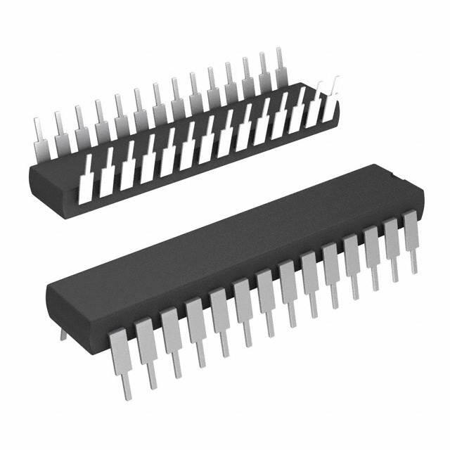


 工商网监
湘ICP备2023018690号
工商网监
湘ICP备2023018690号
