Please note that Cypress is an Infineon Technologies Company.
The document following this cover page is marked as “Cypress” document as this is the
company that originally developed the product. Please note that Infineon will continue
to offer the product to new and existing customers as part of the Infineon product
portfolio.
Continuity of document content
The fact that Infineon offers the following product as part of the Infineon product
portfolio does not lead to any changes to this document. Future revisions will occur
when appropriate, and any changes will be set out on the document history page.
Continuity of ordering part numbers
Infineon continues to support existing part numbers. Please continue to use the
ordering part numbers listed in the datasheet for ordering.
www.infineon.com
�
EZ-PD™ CCG5
USB Type-C Port Controller
EZ-PD™ CCG5, USB Type-C Port Controller
General Description
EZ-PD™ CCG5 is a dual USB Type-C controller that complies with the latest USB Type-C and PD standards. EZ-PD CCG5 provides
a complete dual USB Type-C and USB-Power Delivery port control solution for PCs, notebook, and dock. It can also be used in dual
role and downstream-facing port applications. EZ-PD CCG5 uses Cypress’ proprietary M0WS8 technology with a 32-bit, 48-MHz
Arm® Cortex®-M0 processor with 128-KB flash and integrates two complete Type-C Transceivers including the Type-C termination
resistors, RP and RD. CCG5 also integrates high-voltage regulator. CCG5 is available in 40-QFN (1 port[3]) and 96-BGA (2 ports)
packages.
Applications
32-bit MCU Subsystem
■
PCs, Notebook, and Dock
■ Thunderbolt hosts and devices
■
■
■
48-MHz Arm Cortex-M0 CPU
128-KB Flash
12-KB SRAM
Features
Integrated Digital Blocks
Type-C and USB-PD Support
■
Integrated USB Power Delivery (USB-PD) 3.0 support
Two integrated USB-PD Type-C ports
[1]
[2]
■ Integrated UFP (RD) and current sources for DFP (RP) on
both Type-C ports
■ Integrated dead battery termination for DRP (Power
Source/Sink) applications
■ Integrated VCONN FETs to power EMCA cables
■ Integrated fast role swap and extended data messaging
■ Integrated high-voltage LDO, operational up to 21.5 V
■ Integrated 2x USB Analog Mux
■ Integrated 2x SBU Analog Mux
■ Integrated 2x USB Charger detect blocks – BC v1.2, Apple
Charging (source only)
■ Integrated overvoltage protection (OVP) and overcurrent
protection (OCP) on the VBUS
■ Integrated OCP protection on the VCONN
■ Integrated high-voltage protection on CC and SBU pins to
protect against accidental shorts to the VBUS pin on the Type-C
connector
■ Integrated current sense amplifier that supports high-side
current sensing
■ Integrated gate drivers for external VBUS PFET control on
Type-C Ports
■ Supports high-voltage tolerant PFET-controlled GPIOs
■
■
■
Up to two integrated timers and counters to meet response
times required by the USB-PD protocol
Four run-time serial communication blocks (SCBs) with
reconfigurable I2C, SPI, or UART functionality
Clocks and Oscillators
■
Integrated oscillator eliminating the need for an external clock
Low-Power Operation
■
2.75 V to 21.5 V operation
System-Level ESD on CC, D±, and SBU Pins
■
± 8-kV Contact Discharge and ±15-kV Air Gap Discharge based
on IEC61000-4-2 level 4C
Hot-Swappable I/Os
■
Port 1 I2C pins and CC1, CC2 pins are hot-swappable
Packages
■
■
6.0 mm 6.0 mm, 0.6 mm, 40-pin QFN
6.0 mm 6.0 mm, 1.0 mm, 96-ball BGA
Supports industrial temperature range (–40 °C to +85 °C)
Notes
1. UFP refers to Power Sink.
2. DFP refers to Power Source.
3. NRND (Not Recommended for New Designs). Refer to the CCG5C Datasheet for pin to pin compatible replacement part.
Cypress Semiconductor Corporation
Document Number: 002-17682 Rev. *M
•
198 Champion Court
•
San Jose, CA 95134-1709
•
408-943-2600
Revised March 28, 2019
�EZ-PD™ CCG5
Logic Block Diagram
CCG5: Single- Chip Type- C Controller
Flash
(128KB)
SRAM
(12KB )
System
Resources
2x SBU Analog
Mux Switch
2x2 USB Analog
Mux Switch
2x USB Charge
Detect
Document Number: 002-17682 Rev. *M
Advanced High- Performance Bus
(AHB)
CORTEX -M0
48 MHz
2x TCPWM
High- Side Current
sense Amplifier
ARM
Integrated Digital Blocks
SCB
(I2 C, SPI, UART)
SCB
(I2 C, SPI, UART)
SCB
(I2 C, SPI, UART)
SCB
(I2 C, SPI, UART)
I/O Subsystem
Programmable I/O Matrix
MCU Subsystem
CC
VCONN
28 GPIO
Pins
USB PD Subsystem x2
Baseband MAC
VBUS OVP
Protection
Baseband PHY
HV Protection
On CC & SBU
Hi- Voltage LDO
( 21.5V)
Under Voltage
Protection
1x 8- bit SAR ADC
2x VCONN FETs
VBUS/VCONN OCP
Protection
2x Gate Drivers
Page 2 of 43
�EZ-PD™ CCG5
Contents
Functional Overview ........................................................ 4
USB-PD Subsystem (SS) ............................................ 4
CPU and Memory Subsystem ..................................... 6
Power System Overview .................................................. 7
Peripherals .................................................................. 8
GPIO ........................................................................... 8
Pinouts .............................................................................. 9
Application Diagrams ..................................................... 16
Electrical Specifications ................................................ 21
Absolute Maximum Ratings ....................................... 21
Device-Level Specifications ...................................... 22
Digital Peripherals ..................................................... 25
System Resources .................................................... 26
Document Number: 002-17682 Rev. *M
Ordering Information ...................................................... 34
Ordering Code Definitions ......................................... 34
Packaging ........................................................................ 35
Acronyms ........................................................................ 37
Document Conventions ................................................. 38
Units of Measure ....................................................... 38
References and Links To Applications Collaterals .... 39
Document History Page ................................................. 40
Sales, Solutions, and Legal Information ...................... 43
Worldwide Sales and Design Support ....................... 43
Products .................................................................... 43
PSoC® Solutions ...................................................... 43
Cypress Developer Community ................................. 43
Technical Support ..................................................... 43
Page 3 of 43
�EZ-PD™ CCG5
Functional Overview
USB-PD Subsystem (SS)
USB-PD Physical Layer
The CCG5 has two USB-PD subsystems consisting of the
USB-PD physical layer (PHY) block and supporting circuits. The
USB-PD PHY consists of a transmitter and receiver that communicate BMC and 4b/5b encoded data over the CC channel based
on the PD 3.0 standard. All communication is half-duplex. The
PHY practices collision avoidance to minimize communication
errors on the channel.
In addition, the CCG5 USB-PD block includes all termination
resistors (RP and RD) and their switches as required by the USB
Type-C spec. RP and RD resistors are required to implement
connection detection, plug orientation detection, and for establishing the USB source/sink roles.
The integrated RP resistor enables CCG5 to be configured as a
DFP. The RP resistor is implemented as a current source and can
be programmed to support the complete range of current
capacity on the VBUS defined in the USB Type-C Spec.
To support the latest USB-PD 3.0 specification, CCG5 has implemented the Fast Role Swap (FRS) feature. The FRS feature
enables externally powered docks and hubs to rapidly switch to
bus power when their external power supply is removed. CCG5
also supports DeepSleep in notebook systems where CCG5 is
expecting FRS detection.
For more details, refer to Section 6.3.17 in the USB-PD 3.0
specification.
CCG5 is designed to be fully interoperable with revision 3.0 of
the USB Power Delivery specification as well as revision 2.0 of
the USB Power Delivery specification.
CCG5 supports Extended Messages containing data of up to 260
bytes. The Extended Messages will be larger than expected by
the USB-PD 2.0 hardware. To accommodate Revision 2.0 based
systems, a Chunking mechanism is implemented such that
messages are limited to Revision 2.0 sizes unless it is
discovered that both systems support longer message lengths.
The RD resistor is used to identify CCG5 as a UFP in a DRP
application. The RD resistor on CC pins is required even when
the part is not powered for dead battery termination detection
and charging.
Figure 1. USB-PD Subsystem
To/From System Resources
vref
iref
To/ from AHB
8-bit ADC
From AMUX
VCONN FET Enable
V5V
TxRx Enable
VCONN
FETs
Digital Baseband PHY
Tx_data
from AHB
Enable Logic
Tx
SRAM
4b5b
Encoder
SOP
Insert
BMC
Encoder
Rp
TX
CRC
Rx_data
to AHB
CC1
RX
Rx
SRAM
4b5b
Decoder
SOP
Detect
CC2
Comp
CC control
CC detect
Deep Sleep Reference Enable
Functional, Wakeup Interrupts
Document Number: 002-17682 Rev. *M
RD1
BMC
Decoder
Deep Sleep Vref &
Iref Gen (common
for both ports)
Ref
Active
Rd
Analog Baseband PHY
vref, iref
DB
Rd
RD2
8kV IEC ESD
RD1 shorted to CC1 and RD2 shorted to CC2 for DRP applications using
bondwire. For DFP applications, RD1 and RD2 not shorted to CC1 and CC2.
Dead Battery (DB) Rd termination removed after MCU boots up
Page 4 of 43
�EZ-PD™ CCG5
VCONN FET
SBU Mux
CCG5 has two power supply inputs, V5V_P1 and V5V_P2 pins,
for providing power to EMCA cables through integrated VCONN
FETs. There are two VCONN FETs for each PD port to power
either CC1 or CC2 pins. These FETs can provide 1.5-W power
over VCONN on the CC1 and CC2 pins for the EMCA cables.
CCG5 also supports integrated OCP on VCONN.
The SBU switch mux contains 2x1 Mux and a single 2x2 cross
bar SBU switch per the Type-C port. The 2x1 MUX enables you
to select between the Display Port or Thunderbolt alternate
mode and the single-ended 2x2 switch enables you to route
signals to the appropriate SBU1/2 based on CC (Type-C plug)
orientation.
ADC
The USB-PD subsystem contains one 8-bit successive approximation register (SAR) for analog-to-digital conversions (ADC).
The ADCs include an 8-bit DAC and a comparator. The DAC
output forms the positive input of the comparator. The negative
input of the comparator is from a 4-input multiplexer. The four
inputs of the multiplexer are a pair of global analog multiplex
busses, an internal bandgap voltage, and an internal voltage
proportional to the absolute temperature. All GPIOs on the chip
have access to the ADCs through the chip-wide analog mux bus.
The CC1 and CC2 pins of both Type-C ports are not available to
connect to the mux bus.
The AUX port of the SBU switch supports only differential
signals. Non-differential signals on the AUX port cause signal
coupling at the output of the SBU switch. The LS port of the SBU
switch supports both non-differential and differential signals.
Figure 2. CCG5 SBU Crossbar Switch Block Diagram
USB HS Mux
The HS Mux contains a 2×2 cross bar switch to route the system
D± lines to the Type-C top or bottom ports based on the CC
(Type-C plug) orientation. The unused D± top or bottom lines can
be connected to a UART (Debug) port. The maximum operating
frequency of UART must be 1 Mbps.
The HS Mux also contains charger detection/emulation for
detecting USB BC 1.2 (source only) and Apple terminations. The
charger detection block is connected to the D± from the system
as shown in Figure 3.
To meet the HS eye diagram requirements with sufficient margin,
follow these guidelines:
■
It is recommended to keep the total USB HS signal trace
lengths (USB 2.0 host to CCG5 + CCG5 to Type-C connector
pins) to 4 inches.
■
Total USB HS signal trace lengths can be increased up to 8
inches by adjusting the drive strength on the USB 2.0 host.
■
The differential impedance across the DP/DM signal traces
shall be 90 Ω.
■
Trace width shall be 6 mils.
■
Air Gap (distance between lines) shall be 8 mils.
Figure 3. CCG5 DP/DM Switch Block Diagram
Overvoltage and Undervoltage Protection on VBUS
Overcurrent Protection on VBUS
CCG5 implements an undervoltage/overvoltage (UV/OV)
detection circuit for the VBUS supply. The threshold for OV and
UV detection can be set independently. Both UV and OV detector
have programmable thresholds and is controlled by the
firmware.
CCG5 integrates a high-side current sense amplifier to detect
overcurrent on the VBUS. Overcurrent protection is enabled by
sensing the current through the 10-m sense resistor connected
between the “CSP_Px” and “CSN_Px” pins.
Document Number: 002-17682 Rev. *M
Page 5 of 43
�EZ-PD™ CCG5
VBUS Discharge
CCG5 also has integrated VBUS discharge FETs and resistors
for each port. It is used to discharge VBUS to meet the USB-PD
specification timing on a detach condition and negative voltage
transition.
VBUS Regulator
CCG5 can operate from three power supplies – VSYS, VBUS_P1,
and VBUS_P2. CCG5 integrates the regulator (that supports up to
21.5 V) to derive operating supply voltage. The VSYS always
takes priority over VBUS_P1/VBUS_P2. In the absence of VSYS,
the regulator powers CCG5 either from VBUS_P1 or VBUS_P2.
PFET Gate Driver for VBUS
CCG5 supports the consumer-side and provider-side external
power FET Drivers for PFET. The VBUS_P_CTRL and
VBUS_C_CTRL gate drivers can drive only low or high-Z, thus
requiring an external pull-up. These pins are VBUS
voltage-tolerant.
Charger Detect
CCG5 integrates battery charger emulation and detection for
USB BC.1.2, Apple charge (source only).
IEC Compliant VBUS, CC, D±, and SBU Lines
The chip supports IEC-compliant ESD protection on VBUS, CC,
D±, and SBU lines.
CPU and Memory Subsystem
CPU
The Cortex-M0 CPU in EZ-PD CCG5 is part of the 32-bit MCU
subsystem, which is optimized for low-power operation with
extensive clock gating.
The CPU also includes a serial wire debug (SWD) interface,
which is a 2-wire form of JTAG. The debug configuration used for
EZ-PD CCG5 has four break-point (address) comparators and
two watchpoint (data) comparators.
Flash
The EZ-PD CCG5 device has a flash module with a flash accelerator, tightly coupled to the CPU to improve average access
times from the flash block. The flash block is designed to deliver
two wait states (WS) access time at 48 MHz. The flash accelerator delivers 85% of single-cycle SRAM access performance
on average. Part of the flash module can be used to emulate
EEPROM operation if required.
SROM
A supervisory ROM that contains boot and configuration routines
is provided.
SRAM
CCG5 supports 12-KB SRAM.
High-Voltage Tolerant SBU and CC Lines
The chip supports high-voltage tolerant SBU and CC lines. In the
case of SBU/CC short to VBUS through connectors, these lines
will be protected internally.
Document Number: 002-17682 Rev. *M
Page 6 of 43
�EZ-PD™ CCG5
Power System Overview
Table 1. CCG5 Power Modes
Mode
Description
Figure 4 provides an overview of the EZ-PD CCG5 power
system. CCG5 can operate from three possible external supply
Power is valid and XRES is not asserted. An
sources: VBUS_P1/VBUS_P2 (4 V–21.5 V) or VSYS (2.75 V–5.5 V).
RESET
internal reset source is asserted or Sleep
The VBUS_P1 and VBUS_P2 supply is regulated inside the chip
Controller is sequencing the system out of reset.
with a LDO. The switched supply, VDDD, is either used directly
ACTIVE
Power is valid and CPU is executing instructions.
inside some analog blocks or further regulated down to VCCD,
which powers majority of the core using the regulators. CCG5
Main regulator and most blocks are shut off.
has two different power modes: Active and Deep sleep. TransiDEEP SLEEP Deep Sleep regulator powers logic, but only
tions between these power modes are managed by the power
low-frequency clock if available.
system. A separate power domain, VDDIO, is provided for the
GPIOs. The VDDD and VCCD pins, both outputs of regulators, are
brought out for connecting a 1 µF and 0.1 µF capacitor respectively for the regulator stability only. The VCCD pin is not
supported as a power supply. VDDD can source 2 mA (max) for
external load.
Figure 4. EZ-PD CCG5 Power System
VBUS_P1
LDO
VBUS_P2
LDO
VDDD
VSYS
CC1_P2
CC2_P2
V5V_P2
CC1_P1
CC2_P1
V5V_P1
Core Regulator
(SRSS-Lite)
VDDIO
VCCD
GPIOs
Core
2 x CC
Tx/Rx
VSS
Document Number: 002-17682 Rev. *M
Page 7 of 43
�EZ-PD™ CCG5
Peripherals
GPIO
Serial Communication Blocks (SCB)
EZ-PD CCG5 has 28 GPIOs that includes the I2C and SWD pins,
which can also be used as GPIOs. The I2C pins from only SCB
1 are overvoltage-tolerant. The number of available GPIOs vary
with the part numbers. The GPIO block implements the following:
EZ-PD CCG5 has four SCBs, which can be configured to
implement an I2C, SPI, or UART interface. The hardware I2C
blocks implement full multi-master and slave interfaces capable
of multimaster arbitration. In the SPI mode, the SCB blocks can
be configured to act as a Master/slave.
In the I2C mode, the SCB blocks are capable of operating at
speeds up to 1 Mbps (Fast Mode Plus) and have flexible
buffering options to reduce interrupt overhead and latency for the
CPU. These blocks also support I2C that creates a mailbox
address range in the memory of EZ-PD CCG5 and effectively
reduce I2C communication to reading from and writing to an
array in memory. In addition, the blocks support 8-deep FIFOs
for receive and transmit which, by increasing the time given for
the CPU to read data, greatly reduce the need for clock
stretching caused by the CPU not having read data on time.
The I2C peripherals are compatible with the I2C Standard-mode,
Fast-mode, and Fast-mode Plus devices as defined in the NXP
I2C-bus specification and user manual (UM10204). The I2C bus
I/Os are implemented with GPIO in open-drain modes.
The I2C port on SCB 2, SCB 3 and SCB 4 blocks of EZ-PD CCG5
are not completely compliant with the I2C spec in the following:
■
The GPIO cells for SCB 2 to SCB 4 I2C port are not
overvoltage-tolerant and, therefore, cannot be hot-swapped or
powered up independently of the rest of the I2C system.
■
Fast-mode Plus has an IOL specification of 20 mA at a VOL of
0.4 V. The GPIO cells can sink a maximum of 10-mA IOL with
a VOL maximum of 0.6 V.
■
Fast-mode and Fast-mode Plus specify minimum Fall times,
which are not met with the GPIO cell; Slow strong mode can
help meet this spec depending on the bus load.
■
Seven drive strength modes:
❐ Input only
❐ Weak pull-up with strong pull-down
❐ Strong pull-up with weak pull-down
❐ Open drain with strong pull-down
❐ Open drain with strong pull-up
❐ Strong pull-up with strong pull-down
❐ Weak pull-up with weak pull-down
■
Input threshold select (CMOS or LVTTL)
■
Individual control of input and output buffer enabling/disabling
in addition to the drive strength modes
■
Hold mode for latching previous state (used for retaining I/O
state in Deep Sleep mode)
■
Selectable slew rates for dV/dt related noise control to improve
EMI
During power-on and reset, the I/O pins are forced to the disable
state so as not to crowbar any inputs and/or cause excess
turn-on current. A multiplexing network known as a high-speed
I/O matrix is used to multiplex between various signals that may
connect to an I/O pin.
Timer/Counter/PWM Block (TCPWM)
EZ-PD CCG5 has up to two TCPWM blocks. Each implements
a 16-bit timer, counter, pulse-width modulator (TCPWM), and
quadrature decoder functionality. The block can be used to
measure the period and pulse width of an input signal (timer),
find the number of times a particular event occurs (counter),
generate PWM signals, or decode quadrature signals.
Document Number: 002-17682 Rev. *M
Page 8 of 43
�EZ-PD™ CCG5
Pinouts
Table 2. Pinout for CYPD5125-40LQXIT[4]
Group Name
USB Type-C
Mux
Pin Name
Port
Pin
CC1
Analog
9
CC2
Analog
7
USB PD connector detect/Configuration Channel 2
DPLUS_SYS
Analog
23
USB 2.0 DP from the Host System
DMINUS_SYS
Analog
24
USB 2.0 DM from the Host System
UART_TX/GPIO
P4.0
29
UART TX from Host System/GPIO
UART_RX/GPIO
P4.1
30
UART RX from Host System/GPIO
DPLUS_BOT
Analog
26
USB 2.0 DP from Bottom of Type-C Connector
DMINUS_BOT
Analog
25
USB 2.0 DM from Bottom of Type-C Connector
DMINUS_TOP
Analog
27
USB 2.0 DM from Top of Type-C Connector
DPLUS_TOP
Analog
28
USB 2.0 DP from Top of Type-C Connector
SBU2
Analog
34
Sideband Use signal
SBU1
Analog
35
Sideband Use signal
AUX_P
Analog
36
Auxiliary signal for DisplayPort
AUX_N
Analog
37
Auxiliary signal for DisplayPort
LSTX
Analog
38
Thunderbolt Link Management UART Rx
LSRX
Analog
39
Thunderbolt Link Management UART Tx
VBUS_P_CTRL
Analog
11
Full rail control I/O for enabling/disabling Provider load PFET of
USB Type-C Port 1
0: Path ON
High Z: Path OFF
VBUS_C_CTRL
Analog
12
Full rail control I/O for enabling/disabling Consumer load PFET of
USB Type-C port1
0: Path ON
High Z: Path OFF
VBUS Control
VBUS OCP
GPIOs and Serial
Interfaces
Description
USB PD connector detect/Configuration Channel 1
CSP
Analog
1
Current Sense positive Input for VBUS side external Rsense
CSN
Analog
40
Current sense negative for other side of external Rsense
SWD_IO/AR_RST/GPIO
P1.6
6
SWD I/O/GPIO
SWD_CLK/I2C_CFG_EC/ GPIO
P1.0
2
SWD Clock/ I2C config line.
I2C config line is used to select the I2C address of HPI interface.
The state of line decides the 7 bit I2C address for HPI.
I2C Config Line Floating: 0x08
Pulled up with 1 K: 0x42
Pulled down with 1 K: 0x40
I2C_SDA_SCB2_TBT/GPIO
P1.1
3
SCB2 I2C Data/GPIO
I2C_SCL_SCB2_TBT/GPIO
P1.2
4
SCB2 I2C Clock/GPIO
I2C_INT_TBT/GPIO
P1.3
5
TBT interrupt for port 1/GPIO
OVP_TRIP/I2C_SDA_SCB4/GPIO
P2.4
14
VBUS overvoltage output indicator for port 1/SCB4 I2C Data
UV_OCP_TRIP/I2C_SCL_SCB4/GPIO
P2.3
13
VBUS undervoltage or OCP Output Indicator for Port1 / SCB4 I2C
Clock / GPIO
I2C_SDA_SCB1_EC/GPIO
P5.0
16
SCB1 I2C Data / GPIO
I2C_SCL_SCB1_EC/GPIO
P5.1
17
SCB1 I2C Clock / GPIO
I2C_INT_EC/GPIO
P2.5
15
Embedded Controller interrupt/GPIO
HPD/GPIO
P3.0
18
Hot Plug Detect I/O for port 1/GPIO
I2C_SDA_SCB3 / GPIO / VSEL_2
P3.6
20
SCB3 I2C Data or GPIO or voltage selection control for VBUS
I2C_SCL_SCB3 / GPIO /VSEL_1
P3.7
21
SCB3 I2C Clock or GPIO or voltage selection control for VBUS
Note
4. NRND (Not Recommended for New Designs). Refer to the CCG5C Datasheet for pin to pin compatible replacement part.
Document Number: 002-17682 Rev. *M
Page 9 of 43
�EZ-PD™ CCG5
Table 2. Pinout for CYPD5125-40LQXIT[4] (continued)
Group Name
Pin Name
Port
Pin
Reset
XRES
Analog
10
Description
Reset input (Active LOW)
VBUS
Power
22
VBUS Input for Port 1 (4 V to 21.5 V)
VSYS
Power
19
2.75 V to 5.5 V supply for the system
VDDD
Power
31
VDDD supply output
1. VSYS powered - (Min: VSYS-50 mV) 2.7 V to 5.5 V
2. VBUS powered - 3.15 V to 3.65 V
VDDIO
Power
32
At system-level short the VDDD to VDDIO
Power
Ground
VCCD
Power
33
1.8 V regulator output for filter capacitor. This pin cannot drive
external load.
V5V
Power
8
4.85 V to 5.5 V supply for VCONN FET of Type-C Port 1
VSS
Ground
EPAD
Ground
Note
4. NRND (Not Recommended for New Designs). Refer to the CCG5C Datasheet for pin to pin compatible replacement part.
VDDIO
VDDD
31
VCCD
33
32
SBU1
AUX_P
36
35
34
SBU2
LSTX
AUX_N
37
LSRX
38
CSN
39
1
2
3
4
5
6
7
8
9
10
30
29
28
27
26
25
24
23
22
21
40-Q FN
18
HPD
20
17
I2C_SCL_SCB1_EC
UAR T_RX
UAR T_TX
DPLUS_TO P
DM IN US_TO P
DPLUS_BOT
DM INUS_BO T
DM IN US_SYS
DPLUS_SYS
VBUS
I2C_SCL_SCB3 / VSEL_1
I2C_SDA_SCB3 / VSEL_2
16
I2C_INT_EC
I2C_SDA_SCB1_EC
19
15
OVP_TRIP/I2C_SDA_SCB4 / GPIO
VSYS
14
12
13
UV_OCP_TRIP / I2C_SCL_SCB4 / GPIO
11
VBUS_C_CTRL
(T op View)
VBUS_P_CTRL
C SP
SW D_CLK / I2C_CLK_CFG
I2C_SDA_SC B2_TBT
I2C_SCL_SCB2_TBT
I2C_INT_TBT
SW D_IO/ AR_R ST
CC2
V5V
CC1
XRES
40
Figure 5. 40-Pin QFN Pin Map (Top View) for CYPD5125-40LQXIT[5]
Note
5. NRND (Not Recommended for New Designs). Refer to the CCG5C Datasheet for pin to pin compatible replacement part.
Document Number: 002-17682 Rev. *M
Page 10 of 43
�EZ-PD™ CCG5
Table 3. Pinout for CYPD5225-96BZXI, CYPD5235-96BZXI, and CYPD5236-96BZXI
Group Name
USB Type-C Port 1
USB Type-C Port 2
MUX Type-C Port 1
MUX Type-C Port 2
Pin Name
Port
Ball
Location
CC1_P1
Analog
K2
USB PD connector detect/Configuration Channel 1
CC2_P1
Analog
H2
USB PD connector detect/Configuration Channel 2
CC1_P2
Analog
K9
USB PD connector detect/Configuration Channel 1
CC2_P2
Analog
K10
USB PD connector detect/Configuration Channel 2
Description
AUX_P_P1
Analog
B11
Auxiliary signal for DisplayPort
AUX_N_P1
Analog
C11
Auxiliary signal for DisplayPort
LSRX_P1
Analog
A11
Thunderbolt Link Management UART Rx
LSTX_P1
Analog
A10
Thunderbolt Link Management UART Tx
SBU1_P1
Analog
A3
Sideband Use signal
SBU2_P1
Analog
A4
Sideband Use signal
DMINUS_SYS_P1
Analog
A7
USB 2.0 DM from the Host System
DPLUS_SYS_P1
Analog
A6
USB 2.0 DP from the Host System
UART_RX_P1/GPIO
P4.1
A9
UART Rx from Host System/GPIO
UART_TX_P1/GPIO
P4.0
A8
UART Tx from Host system/GPIO
DMINUS_BOT_P1
Analog
C1
USB 2.0 DM from Bottom of Type-C Connector
DPLUS_BOT_P1
Analog
B1
USB 2.0 DP from Bottom of Type-C Connector
DMINUS_TOP_P1
Analog
A2
USB 2.0 DM from Top of Type-C Connector
DPLUS_TOP_P1
Analog
A1
USB 2.0 DP from Top of Type-C Connector
AUX_P_P2
Analog
D11
Auxiliary signal for DisplayPort
AUX_N_P2
Analog
E11
Auxiliary signal for DisplayPort
LSRX_P2
Analog
L11
Thunderbolt Link Management UART Rx
LSTX_P2
Analog
K11
Thunderbolt Link Management UART Tx
SBU1_P2
Analog
E1
Sideband Use signal
SBU2_P2
Analog
F1
Sideband Use signal
DMINUS_SYS_P2
Analog
G11
USB 2.0 DM from the Host System
DPLUS_SYS_P2
Analog
F11
USB 2.0 DP from the Host System
UART_RX_P2/GPIO
P0.2
J11
UART Rx from Host System/GPIO
UART_TX_P2/GPIO
P0.1
H11
UART Tx from Host system/GPIO
DMINUS_BOT_P2
Analog
L1
USB 2.0 DM from Bottom of Type-C Connector
DPLUS_BOT_P2
Analog
K1
USB 2.0 DP from Bottom of Type-C Connector
DMINUS_TOP_P2
Analog
H1
USB 2.0 DM from Top of Type-C Connector
DPLUS_TOP_P2
Analog
G1
USB 2.0 DP from Top of Type-C Connector
VBUS_P_CTRL_P1
Analog
K3
Full rail control I/O for enabling/disabling Provider load PFET
of USB Type-C Port 1
0: Path ON
High Z: Path OFF
VBUS_C_CTRL_P1
Analog
K4
Full rail control I/O for enabling/disabling Consumer load PFET
of USB Type-C Port 1
0: Path ON
High Z: Path OFF
VBUS Control Type-C
Port1
Document Number: 002-17682 Rev. *M
Page 11 of 43
�EZ-PD™ CCG5
Table 3. Pinout for CYPD5225-96BZXI, CYPD5235-96BZXI, and CYPD5236-96BZXI (continued)
Group Name
Pin Name
Port
Ball
Location
Description
VBUS_P_CTRL_P2
Analog
B4
Full rail control I/O for enabling/disabling Provider load PFET
of USB Type-C Port 2.
0: Path ON
High Z: Path OFF
VBUS_C_CTRL_P2
Analog
B5
Full rail control I/O for enabling/disabling Consumer load PFET
of USB Type-C Port 2.
0: Path ON
High Z: Path OFF
VBUS Control Type-C
Port2
VBUS OCP
GPIOs and Serial
Interfaces
Reset
CSP_P1
Analog
J1
Current Sense Positive Input for P1
CSN_P1
Analog
B3
Current Sense Negative Input for P1
CSP_P2
Analog
L2
Current Sense Positive Input for P2
CSN_P2
Analog
K8
Current Sense Negative Input for P2
GPIO
P3.1
L7
GPIO
I2C_SDA_SCB4/OVP_TRIP_P1/
GPIO
P2.4
K5
VBUS overvoltage output indicator for Port 1 / SCB4 I2C Data/
GPIO
OVP_TRIP_P2 / GPIO
P2.2
L8
VBUS overvoltage output indicator for Port 2 / GPIO
VSEL_1_P2 / GPIO
P0.0
L4
Voltage selection control for VBUS on Port 2 / GPIO
UV_OCP_TRIP_P1/GPIO
P1.4
B6
VBUS undervoltage of OCP output indicator for Port 1/GPIO
HPD_P1/GPIO
P3.0
K7
Hot Plug Detect I/O for Port 1 /GPIO
HPD_P2/GPIO
P3.4
E10
Hot Plug Detect I/O for Port 2 /GPIO
VCONN_OCP_TRIP_P2/
GPIO
P3.3
B9
VCONN OCP output indicator for Port 2 / GPIO
VCONN_OCP_TRIP_P1/GPIO
P3.5
B8
VCONN OCP output indicator for Port 1/ GPIO
UV_OCP_TRIP_P2/GPIO
P1.5
B7
VBUS undervoltage or OCP output indicator for Port 2/GPIO
VSEL_2_P2 / GPIO
P2.0
H10
I2C_SCL_SCB1_EC/
GPIO
Voltage selection control for VBUS on Port 2 / GPIO
P5.1
L6
SCB1 I2C Clock
I2C_SDA_SCB1_EC/
GPIO
P5.0
K6
SCB1 I2C Data
I2C_INT_EC/GPIO
P2.5
L5
I2C interrupt line
I2C_SCL_SCB2_TBT/GPIO
P1.2
E2
SCB2 I2C Clock/GPIO
I2C_SDA_SCB2_TBT/GPIO
P1.1
D2
SCB2 I2C Data /GPIO
I2C_INT_TBT_P1/GPIO
P1.3
F2
I2C interrupt line/GPIO
I2C_INT_TBT_P2/GPIO
P2.1
G2
I2C interrupt line
I2C_SCL_SCB3 / VSEL_1_P1
/GPIO
P3.7
L10
SCB3 I2C Clock/ Voltage selection control for VBUS on Port 1/
GPIO
I2C_SDA_SCB3 / VSEL_2_P1 /
GPIO
P3.6
J10
SCB3 I2C Data / Voltage selection control for VBUS on Port 1
/GPIO
I2C_SCL_SCB4/GPIO
P2.3
F10
SCB4 I2C Clock /GPIO
I2C_SDA_SCB4/GPIO
P3.2
G10
SCB4 I2C Data /GPIO
SWD_IO/AR_RST# /GPIO
P1.6
B2
SWD I/O / AR Reset / GPIO
SWD_CLK/I2C_CFG_EC/GPIO
P1.0
C2
SWD Clock / I2C config line / GPIO.
I2C config line is used to select the I2C address of HPI interface.
The state of line decides the 7 bit I2C address for HPI.
I2C Config Line Floating: 0x08
Pulled up with 1 K: 0x42
Pulled down with 1 K: 0x40
XRES
Analog
H6
Reset input (Active LOW)
Document Number: 002-17682 Rev. *M
Page 12 of 43
�EZ-PD™ CCG5
Table 3. Pinout for CYPD5225-96BZXI, CYPD5235-96BZXI, and CYPD5236-96BZXI (continued)
Group Name
Pin Name
Port
Ball
Location
VBUS_P1
Power
D1
VBUS Input for Port 1 (4 V to 21.5 V)
VBUS_P2
Power
L3
VBUS Input for Port 2 (4 V to 21.5 V)
VSYS
Power
A5
2.75 V to 5.5 V supply for the system
VDDD
Power
D10
VDDD supply output
1. VSYS powered - (Min: VSYS-50 mV) 2.7 V to 5.5 V
2. VBUS powered - 3.15 V to 3.65 V
VCCD
Power
B10
1.8 V regulator output for filter capacitor. This pin cannot drive
external load.
At system-level short the VDDD to VDDIO
Power
Ground
No Connect
Description
VDDIO
Power
C10
V5V_P1
Power
J2
4.85 V to 5.5 V supply for VCONN FET of Type-C Port 1
V5V_P2
Power
L9
4.85 V to 5.5 V supply for VCONN FET of Type-C Port 2
GND
Ground
D5
Ground
GND
Ground
D6
Ground
GND
Ground
D7
Ground
GND
Ground
D8
Ground
GND
Ground
E4
Ground
GND
Ground
E5
Ground
GND
Ground
E6
Ground
GND
Ground
E7
Ground
GND
Ground
E8
Ground
GND
Ground
F4
Ground
GND
Ground
F5
Ground
GND
Ground
F6
Ground
GND
Ground
F7
Ground
GND
Ground
F8
Ground
GND
Ground
G4
Ground
GND
Ground
G5
Ground
GND
Ground
G6
Ground
GND
Ground
G7
Ground
GND
Ground
H7
Ground
NC
DNU
G8
Not Connect
NC
DNU
H4
Not Connect
NC
DNU
H5
Not Connect
NC
DNU
H8
Not Connect
Document Number: 002-17682 Rev. *M
Page 13 of 43
�EZ-PD™ CCG5
Figure 6. 96-Pin BGA Pin Map for CYPD5225-96BXZI, CYPD5235-96BZXI, and CYPD5236-96BZXI
1
2
A
DPLUS_TO DMINUS_TOP
P_P1
_P1
B
DPLUS_BO
T_P1
SWD_DATA/
TBT_RST# /
P1.6
C
DMINUS_B
OT_P1
SWD_CLK/
I2C_CFG_EC/
P1.0
D
VBUS_P1
I2C_SDA_SC
B2_TBT/
P1.1
E
SBU1_P2
I2C_SCL_SCB
2_TBT/
P1.2
F
SBU2_P2
3
4
5
6
SBU1_P1
SBU2_P1
VSYS
DPLUS_SY
S_P1
CSN_P1
7
8
9
DMINUS_S UART_Tx_P UART_Rx_
YS_P1
1 / P4.0
P1 / P4.1
P1.5 /
P3.5 /
P3.3 /
P1.4 /
VBUS_P_C VBUS_C_CT UV_OCP_T UV_OC_TRI VCON_OCP VCON_OCP
TRL_P2
RL_P2
P_P2
_TRIP_P1
_TRIP_P2
RIP_P1
10
11
LSTx_P1
LSRx_P1
VCCD
AUX_P_P1
VDDIO
AUX_N_P1
GND
GND
GND
GND
VDDD
AUX_P_P2
GND
GND
GND
GND
GND
HPD_P2 /
P3.4
AUX_N_P2
I2C_INT_TBT_
P1/ P1.3
GND
GND
GND
GND
GND
G
DPLUS_TO I2C_INT_TBT_
P_P2
P2/ P2.1
GND
GND
GND
GND
DNU
H
DMINUS_T
OP_P2
CC2_P1
DNU
DNU
XRES
GND
DNU
J
CSP_P1
V5V_P1
K
DPLUS_BO
T_P2
CC1_P1
L
DMINUS_B
OT_P2
CSP_P2
SCL_4 / P2.3 DPLUS_SYS_
P2
SDA_4 /
P3.2
DMINUS_SYS
_P2
VSEL_2_P2/ UART_Tx_P2/
P2.0
P0.1
SDA_3/
VSEL_2_P1/ UART_Rx_P2
/ P0.2
P3.6
VBUS_P_C VBUS_C_C I2C_SDA_S I2C_SDA_S
CB4/OVP_T CB1_EC /
TRL_P1
TRL_P1
P5.0
RIP_P1/P2.4
VBUS_P2
VSEL_1_P2 I2C_INT_EC
/P0.0
/ P2.5
I2C_SCL_S
CB1_EC /
P5.1
HPD_P1 /
P3.0
P3.1
CSN_P2
CC1_P2
CC2_P2
LSTx_P2
OVP_TRIP_
P2/P2.2
V5V_P2
SCL_3 /
VSEL_1_P1/
P3.7
LSRx_P2
Type-C Port
1
Type-C Port
2
Power Pins
GND
GPIOs
Document Number: 002-17682 Rev. *M
Page 14 of 43
�EZ-PD™ CCG5
Table 4 through Table 7 provide the various configuration options for the serial interfaces.
Table 4. Serial Communication Block (SCB1) Configuration
QFN Pin BGA Pin
UART
SPI
I2C
GPIO Functionality
16
K6
–
–
I2C_SDA_SCB1
GPIO
17
L6
–
–
I2C_SCL_SCB1
GPIO
B8
UART_CTS_SCB1
–
–
VCONN OCP output indicator for port 1/
GPIO
20
J10
UART_TX_SCB1
SPI_SEL_SCB1
–
I2C_SDA_SCB3/ VSEL_2_P1 /GPIO
21
L10
UART_RX_SCB1
SPI_MISO_SCB1
–
I2C_SCL_SCB3 / VSEL_1_P1/GPIO
18
K7
UART_RTS_SCB1
–
–
HPD_P1/GPIO
29
A8
–
SPI_MOSI_SCB1
–
UART_TX_P1/GPIO
30
A9
–
SPI_CLK_SCB1
–
UART_RX_P1/GPIO
Note: UART TX and RX of the SCB1 is also the
UART and SPI.
I2C
SDA and SCL of the SCB3. So if SCB 3 is in use, then SCB1 cannot be used for
Table 5. Serial Communication Block (SCB2) Configuration
QFN Pin BGA Pin
UART
SPI Master
I2C Slave
2
C2
UART_RX_SCB2
SPI_SEL_SCB2
–
3
D2
UART_TX_SCB2
SPI_MOSI_SCB2
I2C_SDA_SCB2
4
E2
UART_CTS_SCB2
SPI_MISO_SCB2
I2C_SCL_SCB2
5
F2
UART_RTS_SCB2
SPI_CLK_SCB2
–
GPIO Functionality
SWD_CLK/I2C_CFG_EC/GPIO
I2C_SDA_SCB2_TBT/GPIO
I2C_SCL_SCB2_TBT/GPIO
I2C_INT_TBT_P1/GPIO
Table 6. Serial Communication Block (SCB3) Configuration
QFN Pin BGA Pin
UART
SPI Master
I2C Slave
–
–
I2C_SDA_SCB3
UART_TX_SCB1/VSEL_2_P1 /GPIO
UART_RX_SCB1 / VSEL_1_P1/GPIO
GPIO Functionality
20
J10
21
L10
–
–
I2C_SCL_SCB3
G2
UART_CTS_SCB3
SPI_MISO_SCB3
–
H10
UART_TX_SCB3
SPI_MOSI_SCB3
–
VSEL_2_P2 / GPIO
L4
UART_RX_SCB3
SPI_SEL_SCB3
–
VSEL_1_P2 / GPIO
L8
UART_RTS_SCB3
SPI_CLK_SCB3
–
OVP_TRIP_P2 / GPIO
I2C_INT_TBT_P2/GPIO
Table 7. Serial Communication Block (SCB4) Configuration
QFN Pin BGA Pin
UART
SPI Master
I2C Slave
–
–
I2C_SCL_SCB4
GPIO
GPIO Functionality
13
F10
14
G10
UART_TX_SCB4
SPI_MOSI_SCB4
I2C_SDA_SCB4
GPIO
L7
UART_CTS_SCB4
SPI_MISO_SCB4
–
GPIO
B9
UART_RX_SCB4
SPI_SEL_SCB4
–
VCONN_OCP_TRIP_P2/GPIO
E10
UART_RTS_SCB4
SPI_CLK_SCB4
–
HPD_P2/GPIO
Document Number: 002-17682 Rev. *M
Page 15 of 43
�EZ-PD™ CCG5
Application Diagrams
Figure 8 and Figure 9 illustrate the Dual Type-C Port and Single[6] Type-C port Thunderbolt Notebook DRP application diagrams using
a CCG5 device respectively. The Type-C port can be used as a power provider/power consumer.
The CCG5 device communicates with the embedded controller (EC), which manages the Battery Charger Controller (BCC) to control
the charging and discharging of the internal battery. It also updates the Thunderbolt Controller via I2C to route the High-speed signals
coming from the Type-C port to the USB host (during normal mode) or the Graphics processor unit (during Display port Alternate
mode) or the Thunderbolt Host (during Thunderbolt Alternate mode) based on the alternate mode negotiation.
For the dual Type-C notebook application (Figure 8), these Type-C ports can be power providers or power consumers simultaneously.
The CCG5 device controls the transfer of USB 2.0 D± lines from the top and bottom of the Type-C receptacle to the D± lines of the
USB Host controller. CCG5 also handles the routing of SBU1 and SBU2 lines from the Type-C receptacle to the Thunderbolt controller
for the Link management. CCG5 offers ESD Protection on D± and SBU lines as well as VBUS Short protection on SBU and CC lines.
The CCG5 device has an integrated VCONN FET for applications that need to provide power for accessories and cables using the
VCONN pin of the Type-C receptacle. VBUS FETs are also used for providing power over VBUS and for consuming power over VBUS.
The 10-m resistor between the 5-V supply and FETs is used for overcurrent detection on the VBUS. The VBUS_P_CTRL pin of
CCG5 has an in-built VBUS monitoring circuit that can detect OVP and UVP on VBUS.
CCG5 also has an in-built VBUS discharge circuit that is used to quickly discharge VBUS after the Type-C connection is detached.
The internal resistance (as listed in Table 41) of this VBUS discharge circuit is expected to be sufficient for typical CCG5 applications.
However, customers can include an optional VBUS discharge circuit as shown in Figure 7 using any available GPIO. This optional
circuit can be added to the design if the discharge time using the in-built VBUS discharge circuit needs to be further reduced; that is,
VBUS transition time from higher to lower voltages can be further reduced using the external VBUS discharge circuit shown in Figure 7.
This optional external circuit comprises of a N-channel MOSFET and the CCG5 device can be used to enable or disable it as
appropriate.
Figure 7. Optional External VBUS Discharge Circuit
VBUS
200
C C G 5 G P IO P in
(V B U S _ D IS C H A R G E _ P IN )
100 K
Note
6. NRND (Not Recommended for New Designs). Refer to the CCG5C Datasheet for pin to pin compatible replacement part.
Document Number: 002-17682 Rev. *M
Page 16 of 43
�EZ-PD™ CCG5
Figure 8. CCG5 in a Dual Port Notebook Application using CYPD5225-96BZXI
VBUS_OUT_P2
BSC030P03NS3
8
7
6
5
10µF
50V
49.9K
1%
4
5V
0.01
8
7
6
5
3
2
1
VBUS_OUT_P1
5V
BSC030P03NS3
3
2
1
Power
Subsystem
4
Consum er
Path
8
7
6
5
3
2
1
8
7
6
5
3
2
1
49.9K
1%
4
K8
1µF
35V
CSN_P2
10µF
50V
A6
G1
A7
H1
DCC2
CC1
CSP_P1
B6
K1
B7
L1
B5
K10
A5
K9
VBUS_P_CTRL_P1
VBUS_C_CTRL_P1
390pF
4
SWD_CLK/I2C_CFG_EC/P1.0
UART_TX_P1/P4.0
SBU2_P1
SBU2_P2
SBU1_P1
DPLUS_TOP_P1
SBU1_P2
DPLUS_TOP_P2
DMINUS_TOP_P1
DMINUS_TOP_P2
DPLUS_BOT_P1
DPLUS_BOT_P2
DMINUS_BOT_P1
DMINUS_BOT_P2
CC2_P1
CC2_P2
CC1_P1
OVP_TRIP_P2/P2.2
D10
VDDD
C10
VDDIO
3.3V
A5
1µF
10V
VSYS
B10
VCCD
0.1µF
SCL_3/VSEL_1_P1/P3.7
CCG5
(CYPD5225-96BZXI)
96-BGA
UART_TX_P2/P0.1
UART_RX_P2/P0.2
SDA_4/P3.2
SCL_4/P2.3
SDA_3/VSEL_2_P1/P3.6
5V (from System)
J2
UV_OCP_TRIP_P2/P1.5
V5V_P1
L9
GND
VCON_OCP_TRIP_P1/P3.5
V5V_P2
VCON_OCP_TRIP_P2/P3.3
3.3V
UV_OCP_TRIP_P1/P1.4
H6
2.2 K
2.2 K
2.2 K
2.2 K
2.2 K
VSEL_1_P2/P0.0
XRES
0.1µF
VSEL_2_P2/P2.0
2.2 K 2.2 K
L5
Embedded
Controller
NC1
I2C_INT_EC/P2.5
NC2
L6
I2C_SCL_SCB1_EC/P5.1
K6
NC3
I2C_SDA_SCB1_EC/P5.0
E2
I2C_SCL_SCB2_TBT/P1.2
D2
F2
G2
VBUS_OUT_P2
4
A8
X
A9
X
A4
B8
A3
A8
A1
A6
A2
A7
B1
B6
C1
B7
H2
B5
A5
K2
L8
H11
J11
G10
F10
J10
X
X
H10
G8
X
X
H4
X
H5
X
X
X
L7
X
D5, D6, D7, D8, E4, E5,
E6, E7, E8, F4, F5, F6, F7,
F8, G4, G5, G6, G7, H7
3.3V
VBUS_P2
10K
SWD_IO/TBT_RST/P1.6
D11
AUX_N_P2
AUX_N_P1
AUX_P_P2
AUX_P_P1
LSTX_P2
L11
8
GND
X
X
L4
K5
GND
X
X
B9
B6
NC4
P3.1
I2C_INT_TBT_P1/P1.3
Type-C
Receptacle
1
X
X
X
B8
I2C_SDA_SCB4/
OVP_TRIP_P1/P2.4
I2C_SDA_SCB2_TBT/P1.1
100K
K11
CC2
CC1
390pF
VBUS_P1
L3
0.1 µF
D+
D-
X
B7
I2C_INT_TBT_P2/P2.1
D1
0.1 µF
S B U1
D-
X
VBUS_OUT_P1
E11
S B U2
D+
X
L10
H8
3.3V
Data Lines
49.9K
1%
K4
CC1_P2
390pF
0.1 µF
0.1µF
10V
BSC030P03NS3
8
7
6
5
3
2
1
VB US
VDDD
1µF
BSC030P03NS3
8
7
3
2
6
5
1
K3
390pF
Type-C
Receptacle
2
4
1µF
35V
CSN_P1
UART_RX_P1/P4.1
E1
D+
B3
J1
CSP_P2
VBUS_C_CTRL_P2
C2
F1
D-
49.9K
1%
10µF
50V
10µF
50V
VDDD
Note:
CCG5 device s I2C address is determined by SWD_CLK pin.
1K
1K resistors not populated = I2C address 0x08 (default)
1K resistor connected to GND = I2C address 0x40
1K
1K resistor connected to VDDD = I2C address 0x42
A8
D+
L2
VBUS_P_CTRL_P2
S BU2 B8
S BU1
8
7
6
5
3
2
1
4
B4
4
B5
V BUS
1µF
35V
Consumer
Path
BSC030P03NS3
BSC030P03NS3
Provider
Path
BSC030P03NS3
BSC030P03NS3
8
7
3
2
6
5
1
0.01
Provider
Path
1µF
35V
LSTX_P1
LSRX_P2
LSRX_P1
100K
B2
C11
0.1 µF
B11
0.1µF
A10
8
A11
100K
100K
Data Lines
3.3V
3.3V
10K
DNP
E10 HPD_P2/P3.4
HPD_P1/P3.0
D+_SYS_P2
100K
F11
D-_SYS_P2
G11
D+_SYS_P1
D-_SYS_P1
A6
10K
K7 DNP
100K
A7
Note:
Route D+ and D- Host lines to system
USB Host Controller
DPSRC_HPD
DPSRC_HPD
LSRX
LSRX
LSTX
LSTX
DPSRC_AUX_P
DPSRC_AUX_P
DPSRC_AUX_N
DPSRC_AUX_N
RESET_N
Thunderbolt Controller
I2C_SCL
I2C_SDA
I2C_INT_P1
I2C_INT_P2
USB2_D_P
X
Document Number: 002-17682 Rev. *M
USB2_D_N
X
USB2_D_P
X
USB2_D_N
X
Note:
Follow recommendations from manufacturer
for Thunderbolt Controller connections
Page 17 of 43
�EZ-PD™ CCG5
Figure 9 illustrates a Single Port Thunderbolt Notebook DRP application diagram using CYPD5125-40LQXIT[7].
Figure 9. CCG5 in a Single Port Notebook Application using CYPD5125-40LQXIT[7]
VBUS_OUT
5V
BSC030P03NS3
BSC030P03NS3
8
7
6
5
0.01
Provider Path
1 µF
35 V
3
2
1
Power
Subsystem
8
7
6
5
3
2
1
49.9K
1%
4
Consumer Path
Note:
CCG5 device s I2C address is determined by SWD_CLK pin.
1K resistors not populated = I2C address 0x08 (default)
1K resistor connected to GND = I2C address 0x40
1K resistor connected to VDDD = I2C address 0x42
VDDD
CSP
2
CSN
VBUS_P_CTRL
1µF
35V
11
VBUS_C_CTRL
3
2
1
49.9K
1%
4
SWD_CLK/I2C_CFG_EC/P1.0
1 K
BSC030P03NS3
8
7
6
5
BSC030P03NS3
8
3
7
2
6
5
1
1 K
VDDD
4
12
31 VDDD
0.1 µF
VBUS
10 µF
50 V
32 VDDIO
VSYS
UART_TX/P4.0
VCCD
0.1 µF
UART_RX/P4.1
5 V (from System)
SBU2
VCONN_V5V
SBU1
VBUS_OUT
DPLUS_TOP
22 VBUS
3.3 V
10
XRES
0.1µF
2.2 K
2.2 K
DMINUS_TOP
CCG5
[7] DPLUS_BOT
(CYPD5125-40LQXIT )
DMINUS_BOT
40-QFN
CC2
2.2 K
15
EMBEDDED
CONTROLLER
17
16
X
3.3 V
X
X
2.2 K
X
2.2 K
2.2 K
20
21
14
13
4
3
CC1
I2C_INT_EC/P2.5
X
X
B8
35
A8
28
A6
27
A7
26
B6
25
B7
7
B5
A5
9
3.3 V
I2C_SCL_SCB1_EC/P5.1
I2C_SDA_SCB1_EC/P5.0
HPD/P3.0 18
390 pF
390 pF
SBU2
SBU1
D+
DD+
DCC2
CC1
TYPE-C
RECEPTACLE
10 K
DNP
100 K
SDA_3/VSEL_2/P3.6
SCL_3/VSEL_1/P3.7
3.3V
SDA_4/OVP_TRIP/P2.4
SCL_4/UV_OCP_TRIP/P2.3
10 K
SWD_IO/TBT_RST/P1.6
I2C_SCL_SCB2_TBT/P1.2
AUX_N
I2C_SDA_SCB2_TBT/P1.1
AUX_P
5 I2C_INT_TBT/P1.3
41
30
34
LSTX
EPAD
LSRX
DPLUS_SYS
23
DMINUS_SYS
24
Note:
Route D+ and D - Host lines to system
USB Host Controller
100 K
6
DPSRC_HPD
8
RESET_N
37
Data Lines
DPSRC_AUX_N
36
0.1 µF
38
0.1 µF
GND
DPSRC_AUX_P
LSTX
Thunderbolt Controller
39
LSRX
100 K
USB2_D_N
8
29
USB2_D_P
33
I2C_SCL
19
1 µF
I2C_SDA
3.3 V
0.1 µF
I2C_INT_P1
1µF
40
1
10 µF
50 V
4
X
X
Note:
Follow recommendations from manufacturer for
Thunderbolt Controller connections
Note
7. NRND (Not Recommended for New Designs). Refer to the CCG5C Datasheet for pin to pin compatible replacement part.
Document Number: 002-17682 Rev. *M
Page 18 of 43
�EZ-PD™ CCG5
Figure 10 illustrates the Dual Type-C Port Thunderbolt device/dock upstream application diagram using a CCG5 device. The CCG5
device communicates with the power system over I2C, which manages the power provided to the upstream Type-C ports. It also
updates the Thunderbolt Controller over I2C based on the alternate mode negotiation to sink Thunderbolt or USB or DisplayPort Data.
The CCG5 device controls the transfer of USB 2.0 D± lines from the top and bottom of the Type-C receptacle to the D± lines of the
Thunderbolt Controller and Billboard controller. CCG5 also handles the routing of SBU1 and SBU2 lines from the Type-C receptacle
to the Thunderbolt controller for the link management. As mentioned in Features, CCG5 offers ESD Protection on D± and SBU lines
as well as VBUS Short protection on SBU and CC lines.
Figure 10. CCG5 in a Dual port Thunderbolt Device/Dock Upstream Port Application using CYPD5235-96BXZI
VBUS_OUT_P2
VBUS_OUT_P1
0.01
Power
Subsystem
Provider
Path
EN
K8
CSN_P2
B4
B5
L2
CSP_P2
I2C
INT
B7
G10
B6
P1.5
P1.4
SDA_4/P3.2
EN
F10
SCL_4/P2.3
Provider
Path
INT
L7
K5
J1
P3.1 I2C_SDA_SCB4/ CSP_P1
B3
CSN_P1
OVP_TRIP_P1/
P2.4
VBUS_P_CTRL_P2
VBUS_C_CTRL_P2
X
X
D1
0.01
Power
Subsystem
VBUS_P_CTRL_P1
VBUS_C_CTRL_P1
X K3
X K4
L3
VBUS_P2
VBUS_P1
VBUS
VBUS
10µF
50V
VDDD
10µF
50V
1K
C2
SWD_CLK/I2C_CFG_EC/P1.0
1K
SBU1/2_P1
F1, E1
SBU1/2
DP/M_TOP_P1
G1, H1
D+/-_T
DP/M_BOT_P1
K10, K9
B1, C1
D+/-_B
H2, K2
CC1/2
CC1/2_P2
390pF
SCL_3/VSEL_1_P1/P3.7
Type-C
Receptacle
2
D+/ -_T
DP/M_BOT_P2
CC1/2_P1
CC1/2
SBU1/2
A1, A2
DP/M_TOP_P2
K1, L1
D+/-_B
A3, A4
SBU1/2_P2
L10
390pF
X
Type-C
Receptacle
1
VDDD
1µF
D10
VDDD
C10
VDDIO
0.1 µF
3.3V
A5
0.1µF
10V
1µF
10V
CCG5
(CYPD5235-96BZXI)
96-BGA
VSYS
B10
VCCD
0.1µF
SDA_3/VSEL_2_P1/P3.6
VCON_OCP_TRIP_P1/P3.5
5V (from System)
J2
3.3V
B8
X
X
GND
V5V_P1
L9
GND
J10
V5V_P2
H6
XRES
0.1µF
B9
RESET
I2C_SDA/SCL/INT
USB Billboard
(CY7C65215)
NC2
NC3
K6 I2C_SDA_SCB1_EC/P5.0
USB FullSpeed
D-
NC4
H11
UART_TX_P2/P0.1
A8
UART_TX_P1/P4.0
J11
UART_RX_P2/P0.2
A9
UART_RX_P1/P4.1
L4, L8, G2, H10
SPI_Master
D+
SPI_Master
NC1
VCON_OCP_TRIP_P2/P3.3
L5 I2C_INT_EC/P2.5
L6 I2C_SCL_SCB1_EC/P5.1
4
E2
G8
H4
H5
H8
X
X
X
D5, D6, D7, D8, E4, E5,
E6, E7, E8, F4, F5, F6, F7,
F8, G4, G5, G6, G7, H7
GND
I2C_SCL_SCB2_TBT/P1.2
3.3V
D2 I2C_SDA_SCB2_TBT/P1.1
F2
I2C_INT_TBT_P1/P1.3
G2
E11, D11
X
10K
I2C_INT_TBT_P2/P2.1
SWD_IO/TBT_RST/P1.6
AUX_P/N_P2
AUX_P/N_P1
LSTX/RX_P2
LSTX/RX_P1
B2
B11, C11
0.1 µF
0.1 µF
4
K11, L11
A10, A11
8
8
Data Lines
SPI
Slave
Flash
Data Lines
3.3V
3.3V
10K
DNP
E10 HPD_P2/P3.4
HPD_P1/P3.0
D+_SYS_P2
100K
F11
G11
USB2_P
DPSRC_HPD
LSTX/RX
D-_SYS_P2
USB2_N
D+_SYS_P1
D-_SYS_P1
A6
USB2_P
Port B
10K
K7 DNP
100K
A7
USB2_N
DPSRC_HPD
Port A
LSTX/RX
DPSRC_AUX_P/N
DPSRC_AUX_P/N
I2C_SCL
I2C_SDA
4
I2C_INT_P1
Thunderbolt Controller
RESET_N
I2C_INT_P2
SPI_Master
Note:
Follow recommendations from manufacturer
for Thunderbolt Controller connections for
device/dock schematics
Document Number: 002-17682 Rev. *M
Page 19 of 43
�EZ-PD™ CCG5
Figure 11 illustrates the Dual Type-C Port dock downstream application diagram using a CCG5 device. The CCG5 negotiates power
contract with the connected device on the downstream Type-C port and controls the power system. It also controls the data mux via
I2C based on the alternate mode negotiation to source USB SuperSpeed and/or DisplayPort on the downstream Type-C port. As
mentioned above, the CCG5 device offers ESD Protection on D± and SBU lines as well as VBUS Short protection on SBU and CC
lines.
Figure 11. CCG5 in a Dual port Dock Downstream Port Application using CYPD5236-96BXZI
VBUS_OUT_P2
BSC030P03NS3
8
7
6
5
10µF
50V
49.9K
1%
4
5V
0.01
8
7
6
5
3
2
1
VBUS_OUT_P1
5V
BSC030P03NS3
3
2
1
Provider
Path
1µF
35V
Provider
Path
Power
Subsystem
4
K8
X
B5
D1
1µF
35V
J1
CSP_P2
CSP_P1
10µF
50V
4
B3
CSN_P1
VBUS_P_CTRL_P1
VBUS_P_CTRL_P2
VBUS_C_CTRL_P2
8
7
6
5
3
2
1
49.9K
1%
4
L2
CSN_P2
B4
BSC030P03NS3
BSC030P03NS3
8
7
3
2
6
5
1
0.01
K3
K4
VBUS_C_CTRL_P1 X
VBUS_P2
L3
VBUS
VBUS_P1
VBUS
10µF
50V
VDDD
10µF
50V
1K
C2
SWD_CLK/I2C_CFG_EC/P1.0
1K
SBU1/2_P1
F1, E1
SBU1/2
DP/M_TOP_P1
G1, H1
D+/-_T
K1, L1
D+/-_B
A3, A4
SBU1/2
SBU1/2_P2
A1, A2
D+/ -_T
DP/M_TOP_P2
DP/M_BOT_P1
B1, C1
D+/-_B
DP/M_BOT_P2
CC1/2_P1 H2, K2
K10, K9
CC1/2
DS
Type-C
Receptacle
2
OVP_TRIP_P2/P2.2
SCL_3/VSEL_1_P1/P3.7
VDDD
1µF
0.1 µF
3.3V
D10
VDDD
C10
VDDIO
A5
0.1µF
10V
1µF
10V
B10
0.1µF
VSYS
VCCD
CCG5
(CYPD5236-96BZXI)
96-BGA
5V (from System)
J2
L9
GND
H6
3.3V
V5V_P1
XRES
UV_OCP_TRIP_P2/P1.5
H11
UART_TX_P2/P0.1
X
A8
X
UART_TX_P1/P4.0
XJ11 UART_RX_P2/P0.2
A9
UART_RX_P1/P4.1
X
USB2.0 FS
390pF
X
DS
Type-C
Receptacle
1
J10
X
B7
X
B8 X
UV_OCP_TRIP_P1/P1.4
VSEL_1_P2/P0.0
L4 X
VSEL_2_P2/P2.0
H10 X
NC1
K6 I2C_SDA_SCB1_EC/P5.0
X
L10
B6 X
SCL_4/P2.3
VCON_OCP_TRIP_P2/P3.3
L5 I2C_INT_EC/P2.5
L6
I2C_SCL_SCB1_EC/P5.1
L8
VCON_OCP_TRIP_P1/P3.5
SDA_4/P3.2
B9
I2C_SDA/SCL/INT
MCU
Cypress FM0
SDA_3/VSEL_2_P1/P3.6
I2C_SDA_SCB4/
OVP_TRIP_P1/P2.4
V5V_P2
0.1µF
RESET
CC1/2
CC1/2_P2
390pF
K5
GND
X
To Port 1& 2
Data Mux
G10
F10
X G8
NC2
X H4
NC3
X H5
NC4
X H8
D5, D6, D7, D8, E4, E5,
E6, E7, E8, F4, F5, F6, F7,
F8, G4, G5, G6, G7, H7
GND
X E2 I2C_SCL_SCB2_TBT/P1.2
X
X
X
3.3V
D2 I2C_SDA_SCB2_TBT/P1.1
F2
G2
E11, D11
I2C_INT_TBT_P1/P1.3
10K
I2C_INT_TBT_P2/P2.1
SWD_IO/TBT_RST/P1.6
AUX_P/N_P2
AUX_P/N_P1
LSTX/RX_P2
LSTX/RX_P1
B2
B11, C11
0.1 µF
0.1 µF
K11, L11
X
A10, A11
X
8
8
Data Lines
Data Lines
3.3V
3.3V
To P2
DisplayPort
Source
10K
DNP
E10 HPD_P2/P3.4
100K
HPD_P1/P3.0
D+/-_SYS_P2
F11
D+/-_SYS_P1
G11
A6
USB DS 1_HS
10K
K7 DNP
100K
A7
To P1
DisplayPort
Source
USB DS 2_HS
AUX_P/N
AUX_P/N
Port 2
Data Mux
I2C from
CCG5
Full Speed
USB DS 3_HS
I2C from
CCG5
USB3.1 HUB
USB 3.1
USB DS 2_SS
USB DS 1_SS
Port 1
Data Mux
USB 3.1
USB US
From P2
DisplayPort
Source
Document Number: 002-17682 Rev. *M
From Upstream Host
From P1
DisplayPort
Source
Page 20 of 43
�EZ-PD™ CCG5
Electrical Specifications
Absolute Maximum Ratings
Table 8. Absolute Maximum Ratings[8]
Parameter
Description
Min
Typ
Max
Unit
Details/Conditions
VSYS_MAX
Digital supply relative to VSS
–
–
6
V
V5V_P1_MAX
Max supply voltage relative to VSS
–
–
6
V
V5V_P2_MAX
Max supply voltage relative to VSS
–
–
6
V
VBUS_P1_MAX
Max VBUS voltage relative to Vss
–
–
24
V
VBUS_P2_MAX
Max VBUS voltage relative to Vss
–
–
24
V
VDDIO_MAX
Max supply voltage relative to VSS
–
–
VDDD
V
VGPIO_ABS
Inputs to GPIO, DP/DM mux (UART,
SYS, DP/DM_top/bot pins), SBU mux
(AUX, LS, SBU1/2 pins)
–0.5
–
VDDIO + 0.5
V
IGPIO_ABS
Maximum current per GPIO
–25
–
25
mA
IGPIO_INJECTION
GPIO injection current, Max for VIH >
VDDD, and Min for VIL < VSS
–0.5
–
0.5
mA
ESD_HBM
Electrostatic discharge human body
model
2200
–
–
V
Applicable for all pins except
SBU pins
ESD_HBM_SBU[9] Electrostatic discharge human body
model for SBU1, SBU2 pins
1100
–
–
V
Only applicable to SBU pins
Absolute max
Absolute max, current
injected per pin
ESD_CDM
Electrostatic discharge charged
device model
500
–
–
V
–
LU
Pin current for latch up
–200
–
200
mA
–
V
Contact Discharge for
CC1_P1/P2, CC2_P1/P2,
VBUS_P1/P2, SBU1_P1/P2,
SBU2_P1/P2,
DPLUS_TOP/BOT_P1/P2,
DMINUX_TOP/BOT_P1/P2
Air Discharge for
CC1_P1/P2, CC2_P1/P2,
VBUS_P1/P2, SBU1_P1/P2,
SBU2_P1/P2,
DPLUS_TOP/BOT_P1/P2,
DMINUX_TOP/BOT_P1/P2
ESD_IEC_CON
Electrostatic discharge
IEC61000-4-2, contact discharge
ESD_IEC_AIR
Electrostatic discharge
IEC61000-4-2, air discharge
VCC_PIN_ABS
VSBU_PIN_ABS
8000
–
–
15000
–
–
V
Max voltage on CC1 and CC2 pins
–
–
24
V
Max voltage on SBU1 and SBU2 pins
–
–
24
V
–0.5
–
6
V
VGPIO_OVT_ABS OVT GPIO voltage
Absolute max
Absolute maximum for OVT
pins K6 and L6 of BGA, pins
16 and 17 of QFN
Notes
8. Usage above the absolute maximum conditions listed in Table 8 may cause permanent damage to the device. Exposure to absolute maximum conditions for extended
periods of time may affect device reliability. The maximum storage temperature is 150 °C in compliance with JEDEC Standard JESD22-A103, High Temperature
Storage Life. When used below absolute maximum conditions but above normal operating conditions, the device may not operate to specification.
9. JEDEC document JEP155 states that 500 V HBM allows safe manufacturing with a standard ESD control process.
Document Number: 002-17682 Rev. *M
Page 21 of 43
�EZ-PD™ CCG5
Device-Level Specifications
All specifications are valid for –40 °C TA 85 °C and TJ 100 °C, except where noted. Specifications are valid for 3.0 V to 5.5 V
except where noted.
Table 9. DC Specifications
Min
Typ
Max
Unit
SID.PWR#23
Spec ID
VSYS
Power supply input voltage
2.75
–
5.5
V
UFP applications
SID.PWR#23_A
VSYS
Power supply input voltage
3.15
–
5.5
V
DFP/DRP applications
SID.PWR#22
VBUS
VBUS_P1 and VBUS_P2 valid range
4
–
21.5
V
–
SID.PWR#1
VDDD
Regulated output voltage when VSYS is
VSYS – 0.05
powered
–
VSYS
V
SID.PWR#1_A
VDDD
LDO regulated output voltage when
VBUS powered
3.15
–
3.65
V
SID.PWR#26
V5V_P1 and
Power supply Input voltage
V5V_P2
4.85
–
5.5
V
–
SID.PWR#13
VDDIO
GPIO power supply
VDDD
–
VDDD
V
At system-level short the
VDDIO to VDDD
SID.PWR#24
VCCD
Output voltage (for Core Logic)
–
1.8
–
V
–
SID.PWR#15
CEFC
External regulator voltage bypass on
VCCD
80
100
120
nF
SID.PWR#16
CEXC
Power supply decoupling capacitor on
VDDD
–
1
–
µF
SID.PWR#27
CEXV
Power supply decoupling capacitor on
V5V_P1 and V5V_P2
–
0.1
–
µF
SID.PWR#5
IVDDD_EXT
External load current on VDDD either in
Active or Deep Sleep mode
–
1
2
mA –
30
Max LDO current for
powering VDDD and
VDDIO. For powering
mA external circuitry
connected to the chip,
max current is defined by
IVDDD_EXT.
SID.PWR#5A
Parameter
ILDO_MAX
Description
LDO max output current
–
–
Details/Conditions
–
–
X5R ceramic or better
Active Mode, VSYS = 2.75 to 5.5 V. Typical values measured at VSYS = 3.3 V
SID.PWR#4
IDD12
Supply current
–
10
–
TA = 25 °C, CC I/O IN
Transmit or Receive, no
mA I/O sourcing current, CPU
at 24 MHz, two PD ports
active
–
150
–
µA
VSYS = 3.3 V, TA = 25 °C,
–
160
–
µA
VSYS = 3.3 V, TA = 25 °C
for two PD ports
µA
Power source = VSYS,
Type-C not attached, CC
enabled for wakeup, Rp
and Rd connected at
70-ms intervals by CPU.
Rp, Rd connection should
be enabled for both PD
ports.
Deep Sleep Mode, VSYS = 2.75 to 3.6 V
SID34
IDD29
SID34A
IDD29A
SID_DS1
IDD_DS1
VSYS = 2.75 to 3.6 V, I2C, wakeup and
WDT on.
VSYS = 3.3 V, CC wakeup on, Type-C
not connected.
Document Number: 002-17682 Rev. *M
–
150
–
Page 22 of 43
�EZ-PD™ CCG5
Table 9. DC Specifications (continued)
Spec ID
Parameter
SID_DS3
Description
Min
Typ
Max
Unit
Details/Conditions
IDD_DS2
VSYS = 3.3 V, CC wakeup on, DP/DM,
SBU ON with ADC/CSA/UVOV On
–
500
–
µA
IDD_DS1 + DP/DM,
SBU, CC ON,
ADC/CSA/UVOV ON
IDD_XR
Supply current while XRES asserted
–
130
–
µA
Power Source = VSYS =
3.3 V, Type-C not
attached, TA = 25 °C
XRES Current
SID307
Table 10. AC Specifications (Guaranteed by Characterization)
Min
Typ
Max
SID.CLK#4
Spec ID
FCPU
CPU input frequency
–
–
48
SID.PWR#21
TDEEPSLEEP
Wakeup from Deep Sleep mode
–
35
–
SYS.XRES#5
TXRES
External reset pulse width
5
–
–
µs
–
5
25
ms
SYS.FES#1
Parameter
T_PWR_RDY
Description
Power-up to “Ready to accept
command”
I2C/CC
Unit
Details/Conditions
MHz All VDDD
µs
Guaranteed by
characterization.
I/O
Table 11. I/O DC Specifications
Spec ID
Parameter
Description
Min
Typ
Max
Unit
Details/Conditions
0.7 × VDDIO
–
–
V
CMOS input
–
–
0.3 × VDDIO
V
CMOS input
SID.GIO#37
VIH_CMOS
Input voltage HIGH
threshold
SID.GIO#38
VIL_CMOS
Input voltage LOW threshold
SID.GIO#39
VIH_VDDIO2.7-
LVTTL input, VDDIO < 2.7 V 0.7 × VDDIO
–
–
V
–
SID.GIO#40
VIL_VDDIO2.7-
LVTTL input, VDDIO < 2.7 V
–
–
0.3 × VDDIO
V
–
SID.GIO#41
VIH_VDDIO2.7+
LVTTL input, VDDIO 2.7 V
2.0
–
–
V
–
SID.GIO#42
VIL_VDDIO2.7+
LVTTL input, VDDIO 2.7 V
–
–
0.8
V
–
SID.GIO#33
VOH
Output voltage HIGH level
VDDIO – 0.6
–
–
V
IOH = –4 mA at 3 V VDDIO
SID.GIO#34
VOH
Output voltage HIGH level
VDDIO – 0.5
–
–
V
IOH = –1mA at 1.8 V VDDIO
SID.GIO#35
VOL
Output voltage LOW level
–
–
0.6
V
IOL = 4 mA at 1.8 V VDDIO
Output low voltage
–
–
0.4
V
IOL = 3 mA, VDDIO > 2 V
V
IOL = 6 mA, VDDIO > 1.71 V
SID.GIO#35A VOL_I2C_2
0.6
[10]
SID.GIO#35B VOL_I2C_3
Output low voltage
–
–
SID.GIO#35C VOL1_20mA
Output low voltage
–
–
0.4
V
IOL = 20 mA, VDDIO > 3 V, applicable for overvoltage-tolerant
pins only.
SID.GIO#36
VOL
Output voltage LOW level
–
–
0.6
V
IOL = 10 mA (IOL_LED) at 3 V
VDDIO
SID.GIO#5
RPU
Pull-up resistor value
3.5
5.6
8.5
k +25 °C TA, All VDDIO
SID.GIO#6
RPD
Pull-down resistor value
3.5
5.6
8.5
k +25 °C TA, All VDDIO
SID.GIO#16
IIL
Input leakage current
(absolute value)
–
–
2
nA +25 °C TA, 3-V VDDIO
SID.GIO#17
CPIN
Max pin capacitance
–
3
7
pF –
Note
10. In order to drive full bus load at 400 kHz, 6 mA IOL is required at 0.6 V VOL. Parts not meeting this specification can still function, but not at 400 kHz and 400 pF.
Document Number: 002-17682 Rev. *M
Page 23 of 43
�EZ-PD™ CCG5
Table 11. I/O DC Specifications (continued)
Spec ID
Parameter
Description
Min
Typ
Max
Unit
Details/Conditions
SID.GIO#43
VHYSTTL
Input hysteresis, LVTTL
15
40
–
> 2.7 V. Guaranteed by
V
mV DDIO
characterization.
SID.GIO#44
VHYSCMOS
Input hysteresis CMOS
0.05 ×
VDDIO
–
–
mV VDDIO < 4.5 V
Input hysteresis CMOS
200
–
–
mV VDDIO > 4.5 V
SID.GIO#44A VHYSCMOS55
Note
10. In order to drive full bus load at 400 kHz, 6 mA IOL is required at 0.6 V VOL. Parts not meeting this specification can still function, but not at 400 kHz and 400 pF.
Table 12. I/O AC Specifications (Guaranteed by Characterization)
Spec ID
Parameter
Description
SID70
TRISEF
Rise time in Fast Strong mode
SID71
TFALLF
Min
Typ
Max
Unit
Details/Conditions
2
–
12
ns
3.3-V VDDIO, Cload = 25 pF
Fall time in Fast Strong mode
2
–
12
ns
3.3-V VDDIO, Cload = 25 pF
SID.GIO#46 TRISES
Rise time in Slow Strong mode
10
–
60
ns
3.3-V VDDIO, Cload = 25 pF
SID.GIO#47 TFALLS
Fall time in Slow Strong mode
10
–
60
ns
3.3-V VDDIO, Cload = 25 pF
SID.GIO#48 FGPIO_OUT1
GPIO FOUT; 3.3 V VDDIO 5.5 V.
Fast Strong mode.
–
–
16
MHz
SID.GIO#49 FGPIO_OUT2
GPIO FOUT; 1.7 V VDDIO 3.3 V.
Fast Strong mode.
–
–
16
MHz
SID.GIO#50 FGPIO_OUT3
GPIO FOUT; 3.3 V VDDIO 5.5 V.
Slow Strong mode.
–
–
7
MHz
SID.GIO#51 FGPIO_OUT4
GPIO FOUT; 1.7 V VDDIO 3.3 V.
Slow Strong mode.
–
–
3.5
MHz
SID.GIO#52 FGPIO_IN
GPIO input operating frequency;
1.7 V VDDIO 5.5 V.
–
–
16
MHz
90/10%, 25-pF load
90/10%, 25-pF load
90/10%, 25-pF load
90/10%, 25-pF load
90/10% VIO
XRES
Table 13. XRES DC Specifications
Spec ID
Parameter
Description
Min
Typ
Max
Unit
V
CMOS input
SID.XRES#1 VIH
Input voltage HIGH threshold 0.7 × VDDIO
–
–
Details/Conditions
SID.XRES#2 VIL
Input voltage LOW threshold
–
–
0.3 × VDDIO
V
CMOS input
SID.XRES#3 CIN
Input capacitance
–
–
7
pF
–
SID.XRES#4 VHYSXRES
Input voltage hysteresis
–
0.05 × VDDIO
–
mV
Guaranteed by
characterization
Document Number: 002-17682 Rev. *M
Page 24 of 43
�EZ-PD™ CCG5
Digital Peripherals
The following specifications apply to the Timer/Counter/PWM peripherals in the Timer mode.
PWM for GPIO Pins
Table 14. PWM AC Specifications (Guaranteed by Characterization)
Spec ID
Parameter
Description
Min
Typ
Max
Unit
Details/Conditions
–
–
Fc
MHz
Fc max = CLK_SYS.
Maximum = 48 MHz.
TPWMENEXT Input trigger pulse width
2/Fc
–
–
ns
For all trigger events
TPWMEXT
Output trigger pulse width
2/Fc
–
–
ns
Minimum possible width of Overflow,
Underflow, and CC (Counter equals
Compare value) outputs
SID.TCPWM.5A TCRES
Resolution of counter
1/Fc
–
–
ns
Minimum time between successive
counts
SID.TCPWM.5B PWMRES
PWM resolution
1/Fc
–
–
ns
Minimum pulse width of PWM output
SID.TCPWM.5C QRES
Quadrature inputs resolution
1/Fc
–
–
ns
Minimum pulse width between
quadrature-phase inputs
SID.TCPWM.3
TCPWMFREQ Operating frequency
SID.TCPWM.4
SID.TCPWM.5
I2C
Table 15. Fixed I2C AC Specifications
(Guaranteed by Characterization)
Spec ID
SID153
Parameter
FI2C1
Description
Min
Typ
Max
Unit
Details/Conditions
–
–
1
Mbps
–
Bit rate
UART
Table 16. Fixed UART AC Specifications
(Guaranteed by Characterization)
Spec ID
SID162
Parameter
FUART
Description
Min
Typ
Max
Unit
Details/Conditions
–
–
1
Mbps
–
Description
Min
Typ
Max
Unit
Details/Conditions
SPI operating frequency (Master; 6X
oversampling)
–
–
8
MHz
–
Bit rate
SPI
Table 17. Fixed SPI AC Specifications
(Guaranteed by Characterization)
Spec ID
SID166
Parameter
FSPI
Table 18. Fixed SPI Master Mode AC Specifications
(Guaranteed by Characterization)
Description
Min
Typ
Max
Unit
Details/Conditions
SID167
Spec ID
TDMO
Parameter
MOSI valid after SClock driving edge
–
–
15
ns
–
SID168
TDSI
MISO valid before SClock capturing
edge
20
–
–
ns
Full clock, late MISO
sampling
SID169
THMO
Previous MOSI data hold time
0
–
–
ns
Referred to slave capturing
edge
Document Number: 002-17682 Rev. *M
Page 25 of 43
�EZ-PD™ CCG5
Table 19. Fixed SPI Slave Mode AC Specifications
(Guaranteed by Characterization)
Spec ID
Parameter
Description
Min
Typ
Max
Unit
Details/Conditions
SID170
TDMI
MOSI Valid before Sclock capturing
edge
40
–
–
ns
–
SID171
TDSO
MISO Valid after Sclock driving edge
–
–
48 + 3 × TSCB
ns
TSCB = TCPU
SID171A
TDSO_EXT
MISO Valid after Sclock driving edge
in Ext Clk mode
–
–
48
ns
–
SID172
THSO
Previous MISO data hold time
0
–
–
ns
–
SID172A
TSSELSCK
SSEL Valid to first SCK Valid edge
100
–
–
ns
–
Min
Typ
Max
Unit
Memory
Table 20. Flash AC Specifications
Spec ID
Parameter
Description
Details/Conditions
SID.MEM#4
TROW_WRITE
Row (Block) write time (erase and
program)
–
–
20
ms
–
SID.MEM#3
TROW_ERASE
Row erase time
–
–
13
ms
–
SID.MEM#8
TROWPROGRAM
Row program time after erase
–
–
7
ms
25 °C to 55 °C, All VDDD
SID178
TBULKERASE
Bulk erase time (128 KB)
–
–
35
ms
Guaranteed by design
SID180
TDEVPROG
Total device program time
–
–
25
s
Guaranteed by design
SID.MEM#6
FEND
Flash endurance
100k
–
–
cycles
–
SID182
FRET1
Flash retention, TA ≤ 55 °C,
100K P/E cycles
20
–
–
years
–
SID182A
FRET2
Flash retention, TA ≤ 85 °C,
10K P/E cycles
10
–
–
years
–
Min
Typ
Max
System Resources
Power-on-Reset (POR) with Brownout
Table 21. Imprecise Power On Reset (PRES)
Spec ID
Parameter
Description
Unit
SID185
VRISEIPOR
Rising trip voltage
0.80
–
1.50
V
SID186
VFALLIPOR
Falling trip voltage
0.70
–
1.4
V
Details/Conditions
Guaranteed by
characterization
Table 22. Precise Power On Reset (POR) (Guaranteed by Characterization)
Spec ID
Parameter
Description
Min
Typ
Max
Unit
SID190
VFALLPPOR
Brownout Detect (BOD) trip voltage in
active/sleep modes
1.48
–
1.62
V
SID192
VFALLDPSLP
BOD trip voltage in Deep Sleep mode
1.1
–
1.5
V
Document Number: 002-17682 Rev. *M
Details/Conditions
Guaranteed by
characterization
Page 26 of 43
�EZ-PD™ CCG5
SWD Interface
Table 23. SWD Interface Specifications
Spec ID
Parameter
Description
Min
Typ
Max
Unit
Details/Conditions
SID.SWD#1
F_SWDCLK1
3.3 V VDDIO 5.5 V
–
–
14
MHz
SWDCLK 1/3 CPU clock
frequency
SID.SWD#2
F_SWDCLK2
2.7 V VDDIO 3.3 V
–
–
7
MHz
SWDCLK 1/3 CPU clock
frequency
SID.SWD#3
T_SWDI_SETUP T = 1/f SWDCLK
0.25 × T
–
–
ns
SID.SWD#4
T_SWDI_HOLD
0.25 × T
–
–
ns
SID.SWD#5
T_SWDO_VALID T = 1/f SWDCLK
–
–
0.50 × T
ns
SID.SWD#6
T_SWDO_HOLD T = 1/f SWDCLK
1
–
–
ns
T = 1/f SWDCLK
Guaranteed by
characterization
Internal Main Oscillator
Table 24. IMO AC Specifications
(Guaranteed by Design)
Spec ID
Min
Typ
Max
Unit
Frequency variation at 48 MHz
(trimmed)
–
–
±2
%
2.7 V ≤ VDDD < 5.5 V.
–25 °C ≤ TA ≤ 85 °C
SID.CLK#13A FIMOTOLVCCD
Frequency variation at 48 MHz
(trimmed)
–
–
±4
%
All conditions
SID226
TSTARTIMO
IMO start-up time
–
–
7
µs
–
SID.CLK#1
FIMO
IMO frequency
–
48
–
MHz
–
Min
Typ
Max
Unit
Details/Conditions
SID.CLK#13
Parameter
FIMOTOL
Description
Details/Conditions
Internal Low-speed Oscillator
Table 25. ILO AC Specifications
Spec ID
Parameter
Description
SID234
TSTARTILO1
ILO start-up time
–
–
2
ms
SID238
TILODUTY
ILO duty cycle
40
50
60
%
SID.CLK#5
FILO
ILO frequency
20
40
80
kHz
Guaranteed by
characterization
–
Table 26. PD DC Specifications
Spec ID
SID.DC.cc_shvt.1
Parameter
vSwing
Description
Transmitter Output High Voltage
Min
Typ
Max
Unit
Details/Conditions
1.05
–
1.2
V
–
SID.DC.cc_shvt.2
vSwing_low
Transmitter Output Low Voltage
–
0.075
V
–
SID.DC.cc_shvt.3
zDriver
Transmitter output impedance
33
–
75
Ω
–
SID.DC.cc_shvt.4
zBmcRx
Receiver Input Impedance
10
–
MΩ
Guaranteed by design
SID.DC.cc_shvt.5
Idac_std
Source current for USB standard
advertisement
64
–
96
µA
–
SID.DC.cc_shvt.6
Idac_1p5a
Source current for 1.5A at 5 V
advertisement
165.6
–
194.4
µA
–
SID.DC.cc_shvt.7
Idac_3a
Source current for 3A at 5 V
advertisement
303.6
–
356.4
µA
–
SID.DC.cc_shvt.8
Rd
Pull down termination resistance
when acting as UFP (upstream
facing port)
4.59
–
5.61
kΩ
–
Document Number: 002-17682 Rev. *M
Page 27 of 43
�EZ-PD™ CCG5
Table 26. PD DC Specifications (continued)
Spec ID
Min
Typ
Max
Unit
Details/Conditions
Pull down termination resistance
when acting as UFP, with dead
battery (upstream facing port)
4.08
–
6.12
kΩ
–
SID.DC.cc_shvt.10 zOPEN
CC impedance to ground when
disabled
108
–
kΩ
–
SID.DC.cc_shvt.11 DFP_default_0p2
CC voltages on DFP side-Standard
USB
0.15
–
0.25
V
–
SID.DC.cc_shvt.12 DFP_1.5A_0p4
CC voltages on DFP side-1.5A
0.35
–
0.45
V
–
SID.DC.cc_shvt.13 DFP_3A_0p8
CC voltages on DFP side-3A
0.75
–
0.85
V
–
SID.DC.cc_shvt.14 DFP_3A_2p6
CC voltages on DFP side-3A
2.45
–
2.75
V
–
SID.DC.cc_shvt.15 UFP_default_0p66
CC voltages on UFP side-Standard
USB
0.61
–
0.7
V
–
SID.DC.cc_shvt.16 UFP_1.5A_1p23
CC voltages on UFP side-1.5A
1.16
–
1.31
V
–
SID.DC.cc_shvt.17 Vattach_ds
Deep sleep attach threshold
0.3
–
0.6
%
–
SID.DC.cc_shvt.18 Rattach_ds
Deep sleep pull-up resistor
10
–
50
kΩ
–
SID.DC.cc_shvt.30 FS_0p53
Voltage threshold for Fast Swap
Detect
0.49
–
0.58
V
–
Description
Min
Typ
Max
–
8
–
Bits –
SID.DC.cc_shvt.9
Parameter
Description
Rd_db
Analog to Digital Converter
Table 27. ADC DC Specifications
Spec ID
Parameter
Unit
Details/Conditions
SID.ADC.1
Resolution
ADC resolution
SID.ADC.2
INL
Integral non-linearity
–1.5
–
1.5
LSB –
SID.ADC.3
DNL
Differential non-linearity
–2.5
–
2.5
LSB –
SID.ADC.4
Gain Error
Gain error
–1.5
–
1.5
LSB –
SID.ADC.5
VREF_ADC1
Reference voltage of ADC
VDDDmin
–
VDDDmax
V
Reference voltage
generated from
VDDD
SID.ADC.6
VREF_ADC2
Reference voltage of ADC
1.96
2.0
2.04
V
Reference voltage
generate from
bandgap
Document Number: 002-17682 Rev. *M
Page 28 of 43
�EZ-PD™ CCG5
Charger Detect
Table 28. Charger Detect Specifications
Spec ID
Parameter
Description
Min
Typ
Max
Unit
Details/Conditions
DC.CHGDET.1
VDAT_REF
Data detect voltage in charger detect
mode
250
–
400
mV
–
DC.CHGDET.2
VDM_SRC
Dn voltage source in charger detect
mode
500
–
700
mV
–
DC.CHGDET.3
VDP_SRC
Dp voltage source in charger detect
mode
500
–
700
mV
–
DC.CHGDET.4
IDM_SINK
Dn sink current in charger detect
mode
25
–
175
µA
–
DC.CHGDET.5
IDP_SINK
Dp sing current in charger detect
mode
25
–
175
µA
–
DC.CHGDET.6
IDP_SRC
Data contact detect current source
7
–
13
µA
–
DC.CHGDET.27
RDP_UP
Qualcomm pull-up termination on
Dp/Dn
0.9
–
1.575
kΩ
–
DC.CHGDET.32
RDM_UP
Dp/Dn pull-up resistance
0.9
–
1.575
kΩ
–
DC.CHGDET.28
RDP_DWN
Qualcomm pull-down termination on
Dp/Dn
14.25
–
24.8
kΩ
–
DC.CHGDET.31
RDM_DWN
Dp/Dn pull-down resistance
14.25
–
24.8
kΩ
–
DC.CHGDET.29
RDAT_LKG
Data line leakage on Dp/Dn
300
–
500
kΩ
–
DC.CHGDET.34
VSETH
Logic Threshold
1.26
–
1.54
V
–
Table 29. VBUS Regulator AC Specifications
Spec ID
SID.AC.20VREG.1
SID.AC.20VREG.2
Parameter
TSTART
TSTOP
Description
Total start up time for the regulator
supply outputs
Regulator power down time from
vreg_en = 0 to regulator disable
Min
–
Typ
–
Max
Unit
Details/Conditions
µs
Apply VBUS and
measure start time on
VDDD pin.
1
µs
Time from assertion of
an internal disable
signal to for load current
on VDDD to decrease
from 30 mA to 10 μA.
120
–
–
Min
Typ
Max
Unit
Details/Conditions
–
–
1.5
Ω
Measured with a load
current of 5 mA to 10 mA
on VDDD.
Table 30. VSYS Switch Specifications
Spec ID
Parameter
SID.DC.VDDDSW.1 Res_sw
Document Number: 002-17682 Rev. *M
Description
Resistance from supply input to
output supply VDDD
Page 29 of 43
�EZ-PD™ CCG5
Table 31. CSA DC Specifications
Spec ID
Parameter
Min
Typ
Max
Unit
SID.DC.CSA.21 Out_E_Trim_15_DS
Cumulative output Error for Av = 15,
after trim, using Deep sleep
(beta-multiplier) reference
Description
Details/Conditions
–7
–
7
%
–
SID.DC.CSA.22 Out_E_Trim_15_BG
Cumulative output Error for Av = 15,
after trim, using bandgap reference
–4.5
–
4.5
%
–
Cumulative output Error for Av = 100,
SID.DC.CSA.23 Out_E_Trim_100_DS after trim, using Deep sleep (beta-multi- –24.5
plier) reference
–
24.5
%
–
Table 32. UV/OV Specifications
Spec ID
Parameter
Description
Min
Typ
Max
Unit
Details/Conditions
SID.UVOV.1
VTHUVOV1
Voltage threshold accuracy in active
mode using bandgap reference
–
±3
–
%
–
SID.UVOV.2
VTHUVOV2
Voltage threshold accuracy in Deep
Sleep mode using Deep Sleep
reference
–
±5
–
%
–
SID.COMP_ACC
COMP_ACC
Comparator input offset at 4s
–15
–
15
mV
–
Min
Typ
Max
Unit
–
–
5
kΩ
Min
Typ
Max
Unit
–
–
5
Table 33. PFET Gate Driver DC Specifications
Spec ID
SID.DC.PGDO.1
Parameter
Rpd
Description
Resistance when “pull_dn” enabled
Details/Conditions
–
Table 34. PFET Gate Driver AC Specifications
Spec ID
SID.AC.PGDO.2
Parameter
Tr_discharge
Description
Discharge Rate of output note
Details/Conditions
V/µs Guaranteed by design
SBU
Table 35. SBU Switch DC Specifications
Spec ID
Parameter
Description
Min
Typ Max Unit
Details/Conditions
SID.DC.20sbu.1
Ron1
On resistances for Aux switch at 3.3 V input
–
4
7
Ω
–
SID.DC.20sbu.2
Ron2
On resistances for Aux switch at 1 V input
–
3
5
Ω
–
SID.DC.20sbu.4
Ileak1
Pin leakage current for SBU1, SBU2
–4.5
–
4.5
µA –
SID.DC.20sbu.5
Ileak2
Pin leakage current for LSTX, LSRX, AUX_P,
AUX_N
–1
–
1
µA –
SID.DC.20sbu.6
Rpu_aux_1
Pull-up resistance on AUX_P/N
80
–
320
KΩ –
SID.DC.20sbu.7
Rpu_aux_2
Pull-up resistance on AUX_P/N
0.8
–
1.4
MΩ –
SID.DC.20sbu.8
Rpd_aux_1
Pull-down resistance on AUX_P/N
80
–
120
KΩ –
SID.DC.20sbu.9
Rpd_aux_2
Pull-down resistance on AUX_P/N
0.3
–
1.2
MΩ –
SID.DC.20sbu.10 Rpd_aux_3
Pull-down resistance on AUX_P/N
250
–
611
KΩ –
SID.DC.20sbu.11 Rpd_aux_4
Pull-down resistance on AUX_P/N
0.3
–
6.11 MΩ –
SID.DC.20sbu.16 OVP_threshold
Over-voltage protection detection threshold
above VDDIO
200
–
120
0
Document Number: 002-17682 Rev. *M
mV –
Page 30 of 43
�EZ-PD™ CCG5
Table 35. SBU Switch DC Specifications (continued)
Spec ID
Parameter
Description
Min
Typ Max Unit
Details/Conditions
SID.DC.20sbu.17 lsx_ron_3p3
On resistances of LSTX/LSRX to SBU1/2
switch at 3.3 V input
–
8.5
17
Ω
SID.DC.20sbu.18 lsx_ron_1
On resistances of LSTX/LSRX to SBU1/2
switch at 1 V input
–
5.5
11
Ω
SID.DC.20sbu.19 aux_ron_flat_fs
Switch On flat resistances of AUX_P/N to
SBU1/2 switch (from 0 to 3.3 V)
–
–
2.5
Ω
SID.DC.20sbu.20 aux_ron_flat_hs
Switch On flat resistances of AUX_P/N to
SBU1/2 switch (from 0 to 1 V)
–
–
0.5
Ω
SID.DC.20sbu.21 lsx_ron_flat_fs
Switch On flat resistances of LSTX/LSRX to
SBU1/2 switch (from 0 to 3.3 V)
–
–
5
Ω
Guaranteed by design
SID.DC.20sbu.22 lsx_ron_flat_hs
Switch On flat resistances of LSTX/LSRX to
SBU1/2 switch (from 0 to 1 V)
–
–
0.5
Ω
Guaranteed by design
–
–
Guaranteed by design
Guaranteed by design
Table 36. SBU Switch AC Specifications
Spec ID
Parameter
Description
Min
Typ
Max
Unit
Details/Conditions
SID.AC.20sbu.1 Con
Switch ON capacitance
–
–
120
pF
–
SID.AC.20sbu.2 Coff
Switch OFF capacitance - Connector
side
–
–
80
pF
–
SID.AC.20sbu.3 Off_isolation
Switch isolation at F = 1 MHz
–50
–
dB
–
SID.AC.20sbu.4 TON
SBU Switch turn-on time
–
–
200
µs
–
SID.AC.20sbu.5 TOFF
SBU Switch turn-off time
–
–
400
µs
Guaranteed by design
SID.AC.20sbu.6 Off_isolation_tran Coupling on sbu1,2 terminated to
50 ohm, switch-OFF, Rail-to-rail
toggling on LSTX/LSRX
–60
–
60
mV
Guaranteed by design
SID.AC.20sbu.7 X_talk_AC
Cross talk of Switch at F=1 MHz
SBU1/2 to SBU2/1
–50
–
–
dB
Guaranteed by design
SID.AC.20sbu.8 X_talk_tran
Check voltage coupling on SBU2(1)
when Data is transferred from LSTX
(RX) to SBU1 (2)
–70
–
70
mV
Guaranteed by design
Description
Min
Typ
Max
Unit
Table 37. DP/DM Switch DC Specifications
Spec ID
Parameter
Details/Conditions
SID.DC.dpdm.1
Ron_HS
DPDM On resistance for SYS lines (0
to 0.5 V) - HS mode
–
–
8
–
SID.DC.dpdm.2
Ron_FS
DPDM On resistance for SYS lines (0
to 3.3 V) - FS mode
–
–
12
–
SID.DC.dpdm.5
Con_FS
Switch On capacitance at FS at 6 MHz
–
–
50
pF
Guaranteed by design
SID.DC.dpdm.6
Con_HS
Switch on capacitance at HS at
240 MHz
–
–
10
pF
–
SID.DC.dpdm.9
Ileak_pin
pin leakage at DP/DM connector side
and host side
–
–
1
µA
–
SID.DC.dpdm.10
RON_UART
DPDM On resistance for UART lines
(0 to 3.3 V)
–
–
17
–
SID.DC.dpdm.11
RON_FLAT_HS
DPDM On Flat resistance in HS mode
(0 to 0.4 V)
–
–
0.5
Guaranteed by design
Document Number: 002-17682 Rev. *M
Page 31 of 43
�EZ-PD™ CCG5
Table 37. DP/DM Switch DC Specifications (continued)
Spec ID
Parameter
Description
Min
Typ
Max
Unit
Details/Conditions
SID.DC.dpdm.12
RON_FLAT_FS
DPDM On flat resistance in FS mode
(0 to 3.3 V)
–
–
4
Guaranteed by design
SID.DC.dpdm.13
RON_FLAT_UA DPDM UART On flat resistance (0 to
RT
3.3 V)
–
–
4
Guaranteed by design
Details/Conditions
Table 38. DP/DM Switch AC Specifications
Spec ID
Parameter
Description
Min
Typ
Max
Unit
SID.AC.dpdm.5
TON
DP/DM Switch turn-on time
–
–
200
µs
–
SID.AC.dpdm.6
TOFF
DP/DM Switch turn-off time
–
–
0.4
µs
Guaranteed by design
SID.AC.dpdm.7
TON_VPUMP
DP/DM charge pump startup time
–
–
200
µs
Guaranteed by
characterization
SID.AC.dpdm.8
Off_isolation_HS Switch-off isolation for HS
–20
–
–
db
Guaranteed by design
SID.AC.dpdm.9
Off_isolation_FS Switch-off isolation for FS
–50
–
–
db
Guaranteed by design
SID.AC.dpdm.10 X_talk
Cross talk of Switch From FS to HS at
F = 12 MHz
–50
–
–
db
SID.AC.dpdm.11 uart_coupling
peak to peak coupling of UART signal
to DP lines. (UART swinging from 0 to
3.3 V)
–
–
20
mV
Guaranteed by design
Guaranteed by design
Table 39. VCONN Switch DC Specifications
Spec ID
Parameter
Description
Min
Typ
Max
Unit
Details/Conditions
–
1.4
2
–
SID.DC.20VCONN.1
Ron
Switch ON resistance at V5V = 5 V
with 215-mA load current
SID.DC.20VCONN.9
IOCP
Overcurrent detection range for
CC1/CC2
440
–
600
mA
–
SID.DC.20VCONN.10 OVP_threshold
Overvoltage protection detection
threshold above VDDD or V5V
whichever is higher
200
–
1200
mV
–
SID.DC.20VCONN.11 OVP_hysteresis
Overvoltage protection detection
hysteresis
50
–
200
mV
Guaranteed by
design
SID.DC.20VCONN.12 OCP_hysteresis
Overcurrent detection hysteresis
20
–
60
mA
–
Overvoltage protection detection
threshold above V5V of CC1/2,
OVP_threshold_on with CC1 or CC2 switch enabled.
Same threshold triggers reverse
current protection circuit
200
–
700
mV
–
SID.DC.20vconn.14
Document Number: 002-17682 Rev. *M
Page 32 of 43
�EZ-PD™ CCG5
Table 40. VCONN Switch AC Specifications
Min
Typ
Max
Unit
SID.AC.20VCONN.1
Spec ID
TON
Parameter
VCONN switch turn-on time
Description
–
–
200
µs
–
Details/Conditions
SID.AC.20VCONN.2
TOFF
VCONN switch turn-off time
–
–
3
µs
Guaranteed by design
Table 41. VBUS Discharge Specifications
Min
Typ
Max
Unit
SID.VBUS.DISC.1
Spec ID
Ron1
Parameter
20-V NMOS ON resistance
1500
–
3000
–
SID.VBUS.DISC.2
Ron2
20-V NMOS ON resistance
750
–
1500
–
SID.VBUS.DISC.3
Ron3
20-V NMOS ON resistance
500
–
1000
–
SID.VBUS.DISC.4
Ron4
20-V NMOS ON resistance
375
–
750
–
SID.VBUS.DISC.5
Ron5
20-V NMOS ON resistance
300
–
600
–
Document Number: 002-17682 Rev. *M
Description
Details/Conditions
Page 33 of 43
�EZ-PD™ CCG5
Ordering Information
Table 42 lists the EZ-PD CCG5 part numbers and features.
Table 42. EZ-PD CCG5 Ordering Information
Part Number
Battery
Type-C Ports Dead
Termination
Application
CYPD5125-40LQXIT[14] Notebooks, Desktops
CYPD5225-96BZXI
CYPD5225-96BZXIT
CYPD5235-96BZXI
CYPD5235-96BZXIT
CYPD5236-96BZXI
CYPD5236-96BZXIT
Termination
Resistor
Role
Package
1
Yes
RP[11], RD[12], RD-DB[13]
DRP
40-pin QFN
Notebooks, Desktops
2
Yes
RP[11], RD[12], RD-DB[13]
DRP
96-ball BGA
Dock, Upstream port
2
No
RP[11], RD[12]
DRP
96-ball BGA
Dock, Downstream port
2
No
RP[11], RD[12]
DRP
96-ball BGA
Ordering Code Definitions
CY
PD
XX
XX
XX - XX
XX
X
I
T
T = Tape and reel
Temperature Grade : I = Industrial
X = Pb-free
Package Type: XX = FN, LQ, BZ; LQ = QFN; BZ = BGA
Number of pins in the package : XX = 40 or 96
Device Role: Unique combination of role and termination
2X = Dead battery termination , 3X = No Dead battery termination
X5 = Notebooks, desktops, dock applications ,
X6 = Docks for downstream port
Number of Type -C Ports: 1 = 1 Port, 2 = 2 Ports
Product Type : 5 = Fifth -generation product family , CCG5
Marketing Code : PD = Power Delivery product family
Company ID: CY = Cypress
Notes
11. Termination resistor denoting a downstream facing port.
12. Termination resistor denoting an accessory or upstream facing port.
13. Termination resistor denoting dead-battery termination.
14. NRND (Not Recommended for New Designs). Refer to the CCG5C Datasheet for pin to pin compatible replacement part.
Document Number: 002-17682 Rev. *M
Page 34 of 43
�EZ-PD™ CCG5
Packaging
Table 43. Package Characteristics
Description
Conditions
Min
Typ
Max
Unit
TA
Parameter
Operating ambient temperature
Industrial
–40
25
85
°C
TJ
Operating junction temperature
Industrial
–40
25
100
°C
TJA
Package JA (96-ball BGA)
–
–
–
56
°C/W
TJC
Package JC (96-ball BGA)
–
–
–
18.5
°C/W
TJA
Package JA (40-pin QFN)
–
–
–
19.3
°C/W
TJC
Package JC (40-pin QFN)
–
–
–
13.6
°C/W
Table 44. Solder Reflow Peak Temperature
Maximum Peak Temperature
Maximum Time within 5 °C of Peak
Temperature
96-ball BGA
260 °C
30 seconds
40-pin QFN
260 °C
30 seconds
Package
Table 45. Package Moisture Sensitivity Level (MSL), IPC/JEDEC J-STD-2
Package
MSL
96-ball BGA
MSL 3
40-pin QFN
MSL 3
Figure 12. 40-Pin QFN (6 × 6 × 0.6 mm), LR40A/LQ40A 4.6 × 4.6 E-PAD (Sawn) Package Outline, 001-80659
001-80659 *A
Document Number: 002-17682 Rev. *M
Page 35 of 43
�EZ-PD™ CCG5
Figure 13. 96-Ball BGA (6 × 6 × 1.0 mm), Package Outline, 002-10631
E1
2X
0.10 C
E
B
(datum B)
A1 CORNER
A
11 10 9 8 7 6 5 4 3 2 1
7
A1 CORNER
A
B
C
D
E
F
G
H
J
K
L
6
SD
D
0.10 C 2X
eD
6
SE
D1
(datum A)
eE
TOP VIEW
BOTTOM VIEW
DETAIL A
0.10 C
A1
0.08 C
A
C
96XØb
5
SIDE VIEW
Ø0.15 M C A B
Ø0.05 M C
DETAIL A
NOTES:
SYMBOL
1. ALL DIMENSIONS ARE IN MILLIMETERS.
DIMENSIONS
MIN.
NOM.
MAX.
A
-
-
1.00
A1
0.16
-
-
D
6.00 BSC
E
6.00 BSC
D1
5.00 BSC
E1
5.00 BSC
MD
11
ME
11
N
96
b
0.25
0.30
eD
0.50 BSC
eE
0.50 BSC
SD
0.00
SE
0.00
2. SOLDER BALL POSITION DESIGNATION PER JEP95, SECTION 3, SPP-020.
3. "e" REPRESENTS THE SOLDER BALL GRID PITCH.
4. SYMBOL "MD" IS THE BALL MATRIX SIZE IN THE "D" DIRECTION.
SYMBOL "ME" IS THE BALL MATRIX SIZE IN THE "E" DIRECTION.
N IS THE NUMBER OF POPULATED SOLDER BALL POSITIONS FOR MATRIX
SIZE MD X ME.
5. DIMENSION "b" IS MEASURED AT THE MAXIMUM BALL DIAMETER IN A
PLANE PARALLEL TO DATUM C.
6. "SD" AND "SE" ARE MEASURED WITH RESPECT TO DATUMS A AND B AND
DEFINE THE POSITION OF THE CENTER SOLDER BALL IN THE OUTER ROW
0.35
WHEN THERE IS AN ODD NUMBER OF SOLDER BALLS IN THE OUTER ROW
"SD" OR "SE" = 0.
WHEN THERE IS AN EVEN NUMBER OF SOLDER BALLS IN THE OUTER ROW
"SD" = eD/2 AND "SE" = eE/2.
7. A1 CORNER TO BE IDENTIFIED BY CHAMFER, LASER OR INK MARK
METALIZED MARK, INDENTATION OR OTHER MEANS.
8. "+" INDICATES THE THEORETICAL CENTER OF DEPOPULATED SOLDER
BALLS.
9. JEDEC SPECIFICATION NO. REF. : MO-225.
Document Number: 002-17682 Rev. *M
002-10631 *A
Page 36 of 43
�EZ-PD™ CCG5
Acronyms
Table 46. Acronyms Used in this Document (continued)
Table 46. Acronyms Used in this Document
Acronym
Description
ADC
analog-to-digital converter
API
application programming interface
Arm®
advanced RISC machine, a CPU architecture
CC
configuration channel
BOD
Brown out Detect
CPU
central processing unit
CRC
cyclic redundancy check, an error-checking
protocol
CS
Acronym
Description
opamp
operational amplifier
OCP
overcurrent protection
OVP
overvoltage protection
PCB
printed circuit board
PD
power delivery
PGA
programmable gain amplifier
PHY
physical layer
POR
power-on reset
PRES
precise power-on reset
current sense
PSoC®
Programmable System-on-Chip™
DFP
downstream facing port
PWM
pulse-width modulator
DIO
digital input/output, GPIO with only digital
capabilities, no analog. See GPIO.
RAM
random-access memory
DRP
dual role port
RISC
reduced-instruction-set computing
RMS
root-mean-square
RTC
real-time clock
electrically erasable programmable read-only
EEPROM
memory
EMCA
a USB cable that includes an IC that reports cable
characteristics (e.g., current rating) to the Type-C
ports
RX
receive
SAR
successive approximation register
SCL
I2C serial clock
SDA
I2C serial data
S/H
sample and hold
SPI
Serial Peripheral Interface, a communications
protocol
EMI
electromagnetic interference
ESD
electrostatic discharge
FPB
flash patch and breakpoint
FS
full-speed
GPIO
general-purpose input/output
SRAM
static random access memory
IC
integrated circuit
SWD
serial wire debug, a test protocol
IDE
integrated development environment
TX
transmit
Type-C
a new standard with a slimmer USB connector and
a reversible cable, capable of sourcing up to 100 W
of power
UART
Universal Asynchronous Transmitter Receiver, a
communications protocol
USB
Universal Serial Bus
USBIO
USB input/output, CCG5 pins used to connect to a
USB port
XRES
external reset I/O pin
2
I C, or IIC Inter-Integrated Circuit, a communications protocol
ILO
internal low-speed oscillator, see also IMO
IMO
internal main oscillator, see also ILO
I/O
input/output, see also GPIO
LVD
low-voltage detect
LVTTL
low-voltage transistor-transistor logic
MCU
microcontroller unit
NC
no connect
NMI
nonmaskable interrupt
NVIC
nested vectored interrupt controller
Document Number: 002-17682 Rev. *M
Page 37 of 43
�EZ-PD™ CCG5
Document Conventions
Units of Measure
Table 47. Units of Measure (continued)
Table 47. Units of Measure
Symbol
Symbol
Unit of Measure
Unit of Measure
µW
microwatt
milliampere
°C
degrees Celsius
mA
Hz
hertz
ms
millisecond
KB
1024 bytes
mV
millivolt
kHz
kilohertz
nA
nanoampere
k
kilo ohm
ns
nanosecond
Mbps
megabits per second
ohm
MHz
megahertz
pF
picofarad
M
mega-ohm
ppm
parts per million
Msps
megasamples per second
ps
picosecond
µA
microampere
s
second
µF
microfarad
sps
samples per second
µs
microsecond
V
volt
µV
microvolt
Document Number: 002-17682 Rev. *M
Page 38 of 43
�EZ-PD™ CCG5
References and Links To Applications Collaterals
Knowledge Base Articles
■
Key Differences Among EZ-PD™ CCG1, CCG2, CCG3 and
CCG5 - KBA210740
■
Programming EZ-PD™ CCG2, EZ-PD™ CCG3 and EZ-PD™
CCG5 Using PSoC® Programmer and MiniProg3 - KBA96477
■
CCGX Frequently Asked Questions (FAQs) - KBA97244
■
Handling Precautions for CY4501 CCG1 DVK - KBA210560
■
Cypress EZ-PD™ CCGx Hardware - KBA204102
■
Difference between USB Type-C and USB-PD - KBA204033
■
CCGx Programming Methods - KBA97271
■
Getting started with Cypress USB Type-C Products KBA04071
■
■
AN95599 - Hardware Design Guidelines for EZ-PD™ CCG2
■
AN210403 - Hardware Design Guidelines for Dual Role Port
Applications Using EZ-PD™ USB Type-C Controllers
■
AN210771 - Getting Started with EZ-PD™ CCG4
Reference Designs
■
EZ-PD™ CCG2 Electronically Marked Cable Assembly
(EMCA) Paddle Card Reference Design
■
EZ-PD™ CCG2 USB Type-C to DisplayPort Cable Solution
■
CCG1 USB Type-C to DisplayPort Cable Solution
■
CCG1 USB Type-C to HDMI/DVI/VGA Adapter Solution
Type-C to DisplayPort Cable Electrical Requirements
■
EZ-PD™ CCG2 USB Type-C to HDMI Adapter Solution
■
Dead Battery Charging Implementation in USB Type-C
Solutions - KBA97273
■
CCG1 Electronically Marked Cable Assembly (EMCA) Paddle
Card Reference Design
■
Termination Resistors Required for the USB Type-C Connector
– KBA97180
■
CCG1 USB Type-C to Legacy USB Device Cable Paddle Card
Reference Schematics
■
VBUS Bypass Capacitor Recommendation for Type-C Cable
and Type-C to Legacy Cable/Adapter Assemblies – KBA97270
■
EZ-USB GX3 USB Type-C to Gigabit Ethernet Dongle
■
Need for Regulator and Auxiliary Switch in Type-C to
DisplayPort (DP) Cable Solution - KBA97274
■
EZ-PD™ CCG2 USB Type-C Monitor/Dock Solution
■
CCG2 20W Power Adapter Reference Design
■
Need for a USB Billboard Device in Type-C Solutions –
KBA97146
■
CCG2 18W Power Adapter Reference Design
CCG1 Devices in Type-C to Legacy Cable/Adapter Assemblies
– KBA97145
■
■
EZ-USB GX3 USB Type-A to Gigabit Ethernet Reference
Design Kit
■
Cypress USB Type-C Controller Supported Solutions –
KBA97179
■
Kits
■
CY4501 CCG1 Development Kit
Termination Resistors for Type-C to Legacy Ports – KBA97272
■
CY4502 EZ-PD™ CCG2 Development Kit
■
Handling Instructions for CY4502 CCG2 Development Kit –
KBA97916
■
CY4531 EZ-PD CCG3 Evaluation Kit
■
Thunderbolt™ Cable Application Using CCG3 Devices KBA210976
■
CY4541 EZ-PD™ CCG4 Evaluation Kit
■
Power Adapter Application Using CCG3 Devices - KBA210975
■
Methods to Upgrade Firmware on CCG3 Devices - KBA210974
■
Device Flash Memory Size and Advantages - KBA210973
■
Applications of EZ-PD™ CCG4 - KBA210739
Application Notes
■
AN96527 - Designing USB Type-C Products Using Cypress’s
CCG1 Controllers
■
AN95615 - Designing USB 3.1 Type-C Cables Using EZ-PD™
CCG2
Document Number: 002-17682 Rev. *M
Datasheets
■
CCG1 Datasheet: USB Type-C Port Controller with Power
Delivery
■
CYPD1120 Datasheet: USB Power Delivery Alternate Mode
Controller on Type-C
■
CCG2: USB Type-C Port Controller Datasheet
■
CCG3: USB Type-C Controller Datasheet
Page 39 of 43
�EZ-PD™ CCG5
Document History Page
Document Title: EZ-PD™ CCG5, USB Type-C Port Controller
Document Number: 002-17682
Revision
ECN
Orig. of
Change
**
5528106
SOBI
12/07/2016 New datasheet
SOBI
Updated EZ-PD™ CCG5, USB Type-C Port Controller and Features.
Updated Logic Block Diagram.
Updated USB-PD Subsystem (SS) and reordered the Functional Overview
01/27/2017
section.
Updated GPIO.
Updated 40-Pin QFN Pin Map (Top View) for CYPD5125-40LQXIT[5].
SOBI
Changed datasheet status to Preliminary.
Added Errata.
Added Table 4 through Table 7.
Added Table 9 through Table 41 in Device-Level Specifications.
Updated Logic Block Diagram, GPIO, and VBUS Discharge.
06/03/2017
Updated Table 2, Table 3, Table 8, and Table 46.
Updated Figure 5 through Figure 9.
Updated Figure 13 (spec 002-10631 Rev. ** to *A) in Packaging.
Updated compliance with USB spec in Sales, Solutions, and Legal Information.
Updated template.
VGT
Updated USB HS Mux and SBU Mux in Functional Overview.
Updated Flash in CPU and Memory Subsystem.
Updated Power System Overview.
Updated description of BGA pin P2.4 to support SCB4 I2C data.
Changed SID.PWR#1_A; VDDD from 3 V to 3.15 V for DFP application.
Changed SID.AC.dpdm.3; Trise_HS from 630 ps max to 300 ps min.
Changed SID.AC.dpdm.4, Tfall_HS from 630 ps max to 300 ps min.
Updated SID.PWR#23 - changed VSYS to VSYS_UFP and changed range to 2.7 to
5.5 V.
Added SID.PWR#23_A for DFP/DRP application.
Changed max value for SID.20VREG.8, VBUSLOADREG, from 0.2 to 0.3.
Updated SID.ADC.2, SID.ADC.4 to ±1.5.
09/27/2017 Updated SID.PWR#18 description to extend to SBU, DPDM mux pins.
Updated SID.PWR#2 - changed VDDD_MAX to VSYS_MAX.
Removed min value from SID.PWR#14, VDDIO_MAX.
Added min spec of -25mA for SID.PWR#19, Igpio_abs.
Removed ADC.AC spec.
Updated SID.DC.20vconn.11, OVP_hysteresis max.
Added SID.DC.20vconn.14, OVP_threshold_on.
Added SID.AC.dpdm.10, SID.AC.dpdm.11.
Changed min value of SID.AC.dpdm.1, BW_3dB_HS from 1000 to 700.
Changed max value of SID.DC.dpdm.12, SID.DC.dpdm.13 from 4 to 3.
Changed max value of SID.DC.dpdm.2, RON_FS to 12.
Corrected values for SID.AC.dpdm.8, SID.AC.dpdm.9.
Added SID.AC.20sbu.6, SID.AC.20sbu.8, and SID.AC.20sbu.8.
*A
*B
*C
5606273
5694572
5885413
Submission
Date
Document Number: 002-17682 Rev. *M
Description of Change
Page 40 of 43
�EZ-PD™ CCG5
Document Title: EZ-PD™ CCG5, USB Type-C Port Controller
Document Number: 002-17682
*C
(contd.)
*D
5885413
5943992
VGT
Updated SID.DC.20sbu.12, SID.DC.20sbu.15, SID.DC.20sbu.6,
SID.DC.20sbu.7, SID.DC.20sbu.7A, SID.DC.20sbu.8, SID.DC.20sbu.9,
SID.DC.20sbu.10, SID.DC.20sbu.11, SID.DC.20sbu.3, and SID.DC.20sbu.3.
Changed SBU pins ESD voltage to 750 V.
Added new Table 28, new Table 29, Table 43 through Table 45.
09/27/2017
Updated Figure 5, Figure 8, Figure 9.
Added Figure 7.
Removed ADC AC specifications and CSA AC specifications (Table 28 and Table
32 from previous revision).
Removed Errata.
VGT
Added "Thunderbolt hosts and devices" in Applications.
Updated Figure 1 to correctly depict "2 x ADC" for entire CCG5.
Updated description of VDDD pin in Table 2 and Table 3.
Updated the description for pin P2.4 in Table 3.
Added "CYPD5235-96BZXI" and "CYPD5236-96BZXI" part numbers to the
description of Table 3 and Figure 6.
Updated VBUS_P1_MAX and VBUS_P2_MAX values to 24 in Table 8.
Updated min value of ESD_HBM_SBU spec from 750 to 1100 V in Table 8.
Added "Applicable for all pins except SBU pins" in description of "ESD_HBM"
parameter in Table 8.
Updated description of VGPIO_OVT_ABS in Table 8.
Updated description of ESD_IEC_CON and ESD_IEC_AIR parameters in
Table 8.
Changed SID.PWR#13 min value from 1.7 to VDDD in Table 9.
Updated min value of SID.PWR#23 to 2.75 in Table 9.
Updated pin description, values, and details/conditions of parameters
SID.PWR#1 and SID.PWR#1_A to better define VDDD supply in Table 9.
Replace VDDD with VSYS in supply name and conditions for IDD parameters listed
in Table 9.
10/24/2017
Updated Conditions for SID.CLK#4 to “All VDDD” in Table 10.
Removed SID.PWR#20 in Table 10.
Added Guaranteed by Design for SID178 and SID180 in Table 20.
Added description for SID.MEM#8 in Table 20.
Added description for SID.CLK#13 and SID.CLK#13A in Table 24.
Added Guaranteed by Design for SID.DC.cc_shvt.4 in Table 26.
Deleted details and conditions for SID.DC.cc_shvt.14 in Table 26.
Removed SID.DC.cc_SHVT.19 in Table 26.
Updated spec values in Table 32.
Added Guaranteed by Design for SID.AC.PGDO.2 in Table 34.
Added Guaranteed by Design for SID.DC.20sbu.19 through SID.DC.20sbu.22
and removed SID.AC.20sbu.3 in Table 35.
Added Guaranteed by Design for SID.AC.20SBU.5 in Table 36.
Updated max value for SID.AC.20SBU.8 in Table 36.
Removed SID.DC.dpdm.3 and SID.DC.dpdm.4 and added Guaranteed by Design
for SID.DC.dpdm.5 and SID.DC.dpdm.11 through SID.DC.dpdm.13 in Table 37.
Updated SID.DC.dpdm.12 and SID.DC.dpdm.13 max value in Table 37.
Removed SID.AC.dpdm.1, SID.AC.dpdm.2, SID.AC.dpdm.3, and
SID.AC.dpdm.4 in Table 38.
Document Number: 002-17682 Rev. *M
Page 41 of 43
�EZ-PD™ CCG5
Document Title: EZ-PD™ CCG5, USB Type-C Port Controller
Document Number: 002-17682
*D (cont.)
5943992
VGT
Added Guaranteed by Design for SID.AC.dpdm.6, SID.AC.dpdm.7,
SID.AC.dpdm.8, SID.AC.dpdm.9, SID.AC.dpdm.10, and SID.AC.dpdm.13 in
Table 38.
10/24/2017 Added Guaranteed by Design for SID.DC.20VCONN.11 in Table 39.
Removed SID.DC.20VCONN.13 in Table 39.
Added Guaranteed by Design for SID.AC.20VCONN.2 in Table 40.
Updated min value of VSYS to 2.75 throughout the document.
*E
5968629
VGT
11/16/2017
*F
6040630
HPV
02/16/2018 Removed VBUS Regulator DC Specifications.
Updated Figure 8.
Added Figure 10 and Figure 11 and associated content.
Updated pin name and description of P2.4 pin in Table 3.
Updated Power System Overview.
Updated pin name of pin K5 in Figure 6.
03/27/2018
Updated application diagrams in Figure 8, Figure 10, and Figure 11.
Added SID.PWR#5.
Added MPN CYPD5135-40LQXIT in Table 42.
*G
6111610
VGT/AKK
*H
6206852
VGT
06/13/2018
*I
6212870
HPV
06/26/2018 Updated in Typ. value for IDD_DS1 in Table 9.
VGT
Updated Figure 8, Figure 9, Figure 10, and Figure 11.
Updated Table 9.
09/06/2018
Updated min value for SID.DC.20VCONN.9 in Table 39.
Updated Ordering Code Definitions.
*J
*K
6270910
6375937
Added MPNs CYPD5225-96BZXIT, CYPD5235-96BZXIT and
CYPD5236-96BZXIT in Table 42.
SUDH
Updated Electrical Specifications:
Updated Device-Level Specifications:
Updated I/O:
Updated Table 11 (Added VOL_I2C_2, VOL_I2C_3, VOL1_20mA parameters and their
11/27/2018
details).
Added Note 10 and referred the same note in max value of VOL_I2C_3 parameter.
Updated Ordering Information:
Updated Table 42 (Updated part numbers).
*L
6460196
SUDH
Updated Table 2 and Table 3: Updated VDDD Description (“VBUS powered - 3.15
V to 3.6 V” as “VBUS powered - 3.15 V to 3.65 V”).
02/19/2019 Updated Table 9: Updated VDDD Spec Limit to 3.65V.
Updated USB HS Mux.
Updated Copyright information.
*M
6503433
SUDH
03/28/2019
Document Number: 002-17682 Rev. *M
Updated CYPD5125-40LQXI as Not Recommended for New Designs (NRND).
Updated References and Links To Applications Collaterals.
Page 42 of 43
�EZ-PD™ CCG5
Sales, Solutions, and Legal Information
Worldwide Sales and Design Support
Cypress maintains a worldwide network of offices, solution centers, manufacturer’s representatives, and distributors. To find the office
closest to you, visit us at Cypress Locations.
PSoC® Solutions
Products
Arm® Cortex® Microcontrollers
Automotive
cypress.com/arm
cypress.com/automotive
Clocks & Buffers
Interface
cypress.com/clocks
cypress.com/interface
Internet of Things
Memory
cypress.com/iot
cypress.com/memory
Microcontrollers
cypress.com/mcu
PSoC
cypress.com/psoc
Power Management ICs
Cypress Developer Community
Community | Projects | Video | Blogs | Training | Components
Technical Support
cypress.com/support
cypress.com/pmic
Touch Sensing
cypress.com/touch
USB Controllers
Wireless Connectivity
PSoC 1 | PSoC 3 | PSoC 4 | PSoC 5LP | PSoC 6 MCU
cypress.com/usb
cypress.com/wireless
Notice regarding compliance with Universal Serial Bus specification. Cypress offers firmware and hardware solutions that are certified to comply with the Universal Serial Bus specification, USB
Type-C™ Cable and Connector Specification, and other specifications of USB Implementers Forum, Inc (USB-IF). You may use Cypress or third party software tools, including sample code, to modify
the firmware for Cypress USB products. Modification of such firmware could cause the firmware/hardware combination to no longer comply with the relevant USB-IF specification. You are solely
responsible ensuring the compliance of any modifications you make, and you must follow the compliance requirements of USB-IF before using any USB-IF trademarks or logos in connection with any
modifications you make. In addition, if Cypress modifies firmware based on your specifications, then you are responsible for ensuring compliance with any desired standard or specifications as if you
had made the modification. CYPRESS IS NOT RESPONSIBLE IN THE EVENT THAT YOU MODIFY OR HAVE MODIFIED A CERTIFIED CYPRESS PRODUCT AND SUCH MODIFIED PRODUCT
NO LONGER COMPLIES WITH THE RELEVANT USB-IF SPECIFICATIONS.
© Cypress Semiconductor Corporation, 2016-2019. This document is the property of Cypress Semiconductor Corporation and its subsidiaries (“Cypress”). This document, including any software or
firmware included or referenced in this document (“Software”), is owned by Cypress under the intellectual property laws and treaties of the United States and other countries worldwide. Cypress
reserves all rights under such laws and treaties and does not, except as specifically stated in this paragraph, grant any license under its patents, copyrights, trademarks, or other intellectual property
rights. If the Software is not accompanied by a license agreement and you do not otherwise have a written agreement with Cypress governing the use of the Software, then Cypress hereby grants
you a personal, non-exclusive, nontransferable license (without the right to sublicense) (1) under its copyright rights in the Software (a) for Software provided in source code form, to modify and reproduce
the Software solely for use with Cypress hardware products, only internally within your organization, and (b) to distribute the Software in binary code form externally to end users (either directly or
indirectly through resellers and distributors), solely for use on Cypress hardware product units, and (2) under those claims of Cypress's patents that are infringed by the Software (as provided by
Cypress, unmodified) to make, use, distribute, and import the Software solely for use with Cypress hardware products. Any other use, reproduction, modification, translation, or compilation of the
Software is prohibited.
TO THE EXTENT PERMITTED BY APPLICABLE LAW, CYPRESS MAKES NO WARRANTY OF ANY KIND, EXPRESS OR IMPLIED, WITH REGARD TO THIS DOCUMENT OR ANY SOFTWARE
OR ACCOMPANYING HARDWARE, INCLUDING, BUT NOT LIMITED TO, THE IMPLIED WARRANTIES OF MERCHANTABILITY AND FITNESS FOR A PARTICULAR PURPOSE. No computing
device can be absolutely secure. Therefore, despite security measures implemented in Cypress hardware or software products, Cypress shall have no liability arising out of any security breach, such
as unauthorized access to or use of a Cypress product. CYPRESS DOES NOT REPRESENT, WARRANT, OR GUARANTEE THAT CYPRESS PRODUCTS, OR SYSTEMS CREATED USING
CYPRESS PRODUCTS, WILL BE FREE FROM CORRUPTION, ATTACK, VIRUSES, INTERFERENCE, HACKING, DATA LOSS OR THEFT, OR OTHER SECURITY INTRUSION (collectively, "Security
Breach"). Cypress disclaims any liability relating to any Security Breach, and you shall and hereby do release Cypress from any claim, damage, or other liability arising from any Security Breach. In
addition, the products described in these materials may contain design defects or errors known as errata which may cause the product to deviate from published specifications. To the extent permitted
by applicable law, Cypress reserves the right to make changes to this document without further notice. Cypress does not assume any liability arising out of the application or use of any product or
circuit described in this document. Any information provided in this document, including any sample design information or programming code, is provided only for reference purposes. It is the
responsibility of the user of this document to properly design, program, and test the functionality and safety of any application made of this information and any resulting product. "High-Risk Device"
means any device or system whose failure could cause personal injury, death, or property damage. Examples of High-Risk Devices are weapons, nuclear installations, surgical implants, and other
medical devices. “Critical Component” means any component of a High-Risk Device whose failure to perform can be reasonably expected to cause, directly or indirectly, the failure of the High-Risk
Device, or to affect its safety or effectiveness. Cypress is not liable, in whole or in part, and you shall and hereby do release Cypress from any claim, damage, or other liability arising from any use of
a Cypress product as a Critical Component in a High-Risk Device. You shall indemnify and hold Cypress, its directors, officers, employees, agents, affiliates, distributors, and assigns harmless from
and against all claims, costs, damages, and expenses, arising out of any claim, including claims for product liability, personal injury or death, or property damage arising from any use of a Cypress
product as a Critical Component in a High-Risk Device. Cypress products are not intended or authorized for use as a Critical Component in any High-Risk Device except to the limited extent that (i)
Cypress's published data sheet for the product explicitly states Cypress has qualified the product for use in a specific High-Risk Device, or (ii) Cypress has given you advance written authorization to
use the product as a Critical Component in the specific High-Risk Device and you have signed a separate indemnification agreement.
Cypress, the Cypress logo, Spansion, the Spansion logo, and combinations thereof, WICED, PSoC, CapSense, EZ-USB, F-RAM, and Traveo are trademarks or registered trademarks of Cypress in
the United States and other countries. For a more complete list of Cypress trademarks, visit cypress.com. Other names and brands may be claimed as property of their respective owners.
Document Number: 002-17682 Rev. *M
Revised March 28, 2019
Page 43 of 43
�
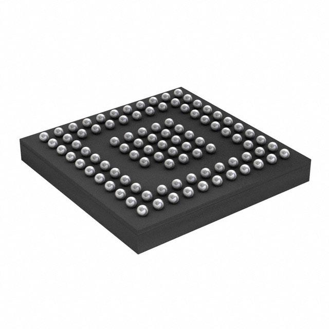


 工商网监
湘ICP备2023018690号
工商网监
湘ICP备2023018690号
