FM4 S6E2G-Series
Pioneer Kit Guide
Doc. # 002-10541 Rev. *F
Cypress Semiconductor
198 Champion Court
San Jose, CA 95134-1709
www.cypress.com
�Copyrights
© Cypress Semiconductor Corporation, 2015-2017. This document is the property of Cypress Semiconductor Corporation
and its subsidiaries, including Spansion LLC (“Cypress”).
This document, including any software or firmware included or
referenced in this document (“Software”), is owned by Cypress under the intellectual property laws and treaties of the
United States and other countries worldwide.
Cypress reserves all rights under such laws and treaties and does not,
except as specifically stated in this paragraph, grant any license under its patents, copyrights, trademarks, or other
intellectual property rights.
If the Software is not accompanied by a license agreement and you do not otherwise have a
written agreement with Cypress governing the use of the Software, then Cypress hereby grants you a personal,
non-exclusive, nontransferable license (without the right to sublicense) (1) under its copyright rights in the Software (a) for
Software provided in source code form, to modify and reproduce the Software solely for use with Cypress hardware
products, only internally within your organization, and (b) to distribute the Software in binary code form externally to end
users (either directly or indirectly through resellers and distributors), solely for use on Cypress hardware product units, and
(2) under those claims of Cypress’s patents that are infringed by the Software (as provided by Cypress, unmodified) to
make, use, distribute, and import the Software solely for use with Cypress hardware products.
Any other use,
reproduction, modification, translation, or compilation of the Software is prohibited.
TO THE EXTENT PERMITTED BY APPLICABLE LAW, CYPRESS MAKES NO WARRANTY OF ANY KIND, EXPRESS
OR IMPLIED, WITH REGARD TO THIS DOCUMENT OR ANY SOFTWARE OR ACCOMPANYING HARDWARE,
INCLUDING, BUT NOT LIMITED TO, THE IMPLIED WARRANTIES OF MERCHANTABILITY AND FITNESS FOR A
PARTICULAR PURPOSE. To the extent permitted by applicable law, Cypress reserves the right to make changes to this
document without further notice. Cypress does not assume any liability arising out of the application or use of any product
or circuit described in this document.
Any information provided in this document, including any sample design information
or programming code, is provided only for reference purposes. It is the responsibility of the user of this document to
properly design, program, and test the functionality and safety of any application made of this information and any resulting
product.
Cypress products are not designed, intended, or authorized for use as critical components in systems designed
or intended for the operation of weapons, weapons systems, nuclear installations, life-support devices or systems, other
medical devices or systems (including resuscitation equipment and surgical implants), pollution control or hazardous
substances management, or other uses where the failure of the device or system could cause personal injury, death, or
property damage (“Unintended Uses”).
A critical component is any component of a device or system whose failure to
perform can be reasonably expected to cause the failure of the device or system, or to affect its safety or effectiveness.
Cypress is not liable, in whole or in part, and you shall and hereby do release Cypress from any claim, damage, or other
liability arising from or related to all Unintended Uses of Cypress products.
You shall indemnify and hold Cypress
harmless from and against all claims, costs, damages, and other liabilities, including claims for personal injury or death,
arising from or related to any Unintended Uses of Cypress products.
Cypress, the Cypress logo, Spansion, the Spansion logo, and combinations thereof, WICED, PSoC, CapSense, EZ-USB,
F-RAM, and Traveo are trademarks or registered trademarks of Cypress in the United States and other countries.
more complete list of Cypress trademarks, visit cypress.com.
For a
Other names and brands may be claimed as property of
their respective owners.
FM4 S6E2G-Series Pioneer Kit Guide, Doc. # 002-10541 Rev. *F
2
�Contents
1.
2.
3.
4.
A.
Introduction.................................................................................................................................................................... 4
1.1
Kit Contents ........................................................................................................................................................... 5
1.2
Board Details ......................................................................................................................................................... 6
1.3
Jumpers and Connectors ...................................................................................................................................... 7
1.4
Getting Started ...................................................................................................................................................... 8
1.5
Additional Learning Resources .............................................................................................................................. 8
1.6
Technical Support.................................................................................................................................................. 8
1.7
Acronyms............................................................................................................................................................... 9
Installation and Test Operation .................................................................................................................................. 10
2.1
Install Software .................................................................................................................................................... 10
2.2
Uninstall Software................................................................................................................................................ 14
2.3
Test Operation ..................................................................................................................................................... 14
Hardware ...................................................................................................................................................................... 23
3.1
System Block Diagram ........................................................................................................................................ 23
3.2
Hardware Features .............................................................................................................................................. 24
3.3
Hardware Details ................................................................................................................................................. 24
Software Development ................................................................................................................................................ 37
4.1
Tool Options ........................................................................................................................................................ 37
4.2
Example Projects................................................................................................................................................. 42
4.3
Flash Programming ............................................................................................................................................. 66
Appendix ...................................................................................................................................................................... 72
A.1
Schematic ............................................................................................................................................................ 72
A.2
Bill of Materials .................................................................................................................................................... 77
Revision History ................................................................................................................................................................... 81
Document Revision History ........................................................................................................................................... 81
FM4 S6E2G-Series Pioneer Kit Guide, Doc. # 002-10541 Rev. *F
3
�1. Introduction
Thank you for your interest in the FM4-176L-S6E2GM FM4 S6E2G-Series Pioneer Kit. The FM4 S6E2G-Series Pioneer Kit
enables customers to evaluate and develop projects using the FM4 device family. Flexible MCU 4 (FM4) is a portfolio of
®
®
high-performance ARM Cortex -M4 MCUs that includes hardware support for digital signal processing and floating-point
operations, designed for safety-critical, industrial systems and home appliance applications. There are multiple series of
device families in this portfolio. The S6E2C-Series, S6E2G-Series and S6E2H-Series are few of the prominent series of
device families. This kit uses a device from the S6E2G-Series.
Devices in the S6E2G-Series are highly integrated 32-bit microcontrollers with high performance and competitive cost. This
series is based on the ARM Cortex-M4 processor, including floating point instructions, with on-chip flash memory and
SRAM. The series has peripherals such as motor control timers, A/D converters, and communications interfaces like USB,
CAN, UART, CSIO (SPI), I2C and LIN. The S6E2G-Series of FM4 devices offers up to a 180-MHz CPU, 1MB flash, 192KB
SRAM, 153 GPIOs, 20 communication peripherals, 33 digital peripherals and 3 analog peripherals.
The S6E2G-Series of FM4 devices is designed to meet the high performance requirements of today’s industrial customers.
Such needs not only include the support and enabling of international safety standards but also the inclusion of IoT concepts
for distributed control, to deliver fast, secure and reliable communication interfaces. In order to properly target this high
performance market, the S6E2G-Series Pioneer Kit features the industry standard communication interfaces such as
Ethernet (IEEE 802.3), a full-speed USB Host and a full-speed USB device. The FM4 S6E2G-Series Pioneer Kit offers
footprint compatibility with Arduino™ shields, which provides options for application development. This S6E2G-Series
Pioneer Kit also features multiple on-board sensors like an accelerometer, and a phototransistor, as well as peripherals like
a stereo codec which can be used to quickly prototype data acquisition systems while showcasing external SRAM and Flash
for data logging applications.
In order to properly enable our customers, the FM4 S6E2G-Series Pioneer Kit is aligned to our low cost development
systems, aligning this kit with our successful line of Pioneer Kits in form, price and flexibility.
FM4 S6E2G-Series Pioneer Kit Guide, Doc. # 002-10541 Rev. *F
4
�Introduction
1.1 Kit Contents
The FM4 S6E2G-Series Pioneer Kit contains the following, as shown in Figure 1-1.
FM4 S6E2G-Series Pioneer board
USB Standard-A to Micro-B cable
Quick Start Guide
Figure 1-1. Kit Contents
Inspect the contents of the kit; if you find any part missing, contact your nearest Cypress sales office for help:
www.cypress.com/support.
FM4 S6E2G-Series Pioneer Kit Guide, Doc. # 002-10541 Rev. *F
5
�Introduction
1.2 Board Details
Figure 1-2. FM4 S6E2G-Series Pioneer Kit Markup
FM4 S6E2G-Series Pioneer Kit Guide, Doc. # 002-10541 Rev. *F
6
�Introduction
1.3 Jumpers and Connectors
Table 1-1. Jumper Description
Jumper
J1
J2
Function
Setting
Sets the programming mode of
Open: User mode
MB9AF312K (CMSIS-DAP)
Closed: Serial programming mode
Sets the programming mode of
Open: User mode
S6E2GM
Closed: Serial programming mode
Pin 2 to Pin 1: UART programming mode via UART0
J3
Sets the serial programming
connected to MB9AF312K
mode for the S6E2GM
Pin 2 to Pin 3: USB programming mode
Pin 2 to Pin 1: Power from CMSIS-DAP (CN2)
J4
Sets the power supply source
Pin 2 to Pin 3: Power from USB port of FM4 (CN3)
Table 1-2. Connector Description
Connector
Description
CN1
10-pin JTAG interface
CN2
USB port of CMSIS-DAP (MB9F312K)
CN3
USB port of FM4 MCU
CN4
RJ45 connector
CN5
Headphone jack
CN6
Line-in jack
CN7,CN8,CN9,CN10
Arduino compatible headers
CN11
Microphone jack
CN12, CN13
Multicon connectors
CN14
USB host connector
CN15, CN16, CN17, CN18
Additional GPIO headers
FM4 S6E2G-Series Pioneer Kit Guide, Doc. # 002-10541 Rev. *F
7
�Introduction
1.4 Getting Started
This guide will help you get started with the FM4 S6E2G-Series Pioneer Kit:
The Installation and Test Operation chapter describes the installation of the kit, and the test procedures for testing
the board.
The Hardware chapter describes the major features of the FM4 S6E2G-Series Pioneer Kit and functionalities such
as CMSIS-DAP debugger, Ethernet, USB, stereo codec, memories and sensors.
The Software Development chapter describes how to open and run an example project in the IAR Embedded
Workbench or Keil µVision IDE; it also describes how to use the example projects and how to program devices
using the USB DIRECT Programmer or the FLASH MCU Programmer.
The Appendix provides the kit schematics, and the bill of materials (BOM).
1.5 Additional Learning Resources
Cypress provides a wealth of data at www.cypress.com to help you to select the right MCU device for your design, and to
help you to quickly and effectively integrate the device into your design.
Visit www.cypress.com/FM4-176L-S6E2GM for the following documents of the S6E2G-Series MCU:
Overview: S6E2G-Series fact sheet
Device Selector: Microcontroller Select Guide
Datasheets: S6E2G-Series datasheet and handling precautions.
FM4 Peripheral Manual: Main section, Ethernet section, Communication Macro section, Analog Macro section
and Timer section.
1.6 Technical Support
For assistance, visit Cypress Support or contact customer support at +1(800) 541-4736 Ext. 2 (in the USA) or +1 (408)
943-2600 Ext. 2 (International).
FM4 S6E2G-Series Pioneer Kit Guide, Doc. # 002-10541 Rev. *F
8
�Introduction
1.7 Acronyms
Table 1-3. Acronyms Used in this Document
Acronym
Description
ADC
Analog-to-Digital Converter
CAN
Controlled Acess Network
CMSIS-DAP
Debug Access Port
GPIO
General Purpose Input/Output
I2C
Inter-Integrated Circuit
I2S
Inter-IC Sound
IDE
Integrated Development Environment
IoT
Internet of Things
JTAG
Joint Test Action Group
LDO
Low Drop Out (voltage regulator)
LED
Light-Emitting Diode
LIN
Local Interconnect Network
PDL
Peripheral Driver Library
PWM
Pulse Width Modulation
RGB
Red Green Blue
SPI
Serial Peripheral Interface
SRAM
Static Random Access Memory
SWD
Serial Wire Debug
UART
Universal Asynchronous Receiver Transmitter
USB
Universal Serial Bus
FM4 S6E2G-Series Pioneer Kit Guide, Doc. # 002-10541 Rev. *F
9
�2. Installation and Test Operation
This chapter describes the steps to install the software tools and drivers on a PC for using the FM4 S6E2G-Series Pioneer
Kit. After the successful installation, the user can run the test demo code that was pre-programmed in the device.
2.1 Install Software
Follow these steps to install the FM4 S6E2G-Series Pioneer Kit software:
1.
Download the FM4 S6E2G-Series Pioneer Kit installer from the web page
www.cypress.com/FM4-176L-S6E2GM. The Kit software is available for download in three formats:
FM4 S6E2G-Series Pioneer Kit Complete Setup: This installation package contains the files related to the kit,
including the Documentation, Hardware, Firmware, Software tools and drivers. However, it does not include the
Windows Installer or Microsoft .NET Framework packages. If these packages are not on your computer, the
installer directs you to download and install them from the Internet.
FM4 S6E2G-Series Pioneer Kit Only: This executable file installs only the kit contents, which include kit code
examples, hardware files, and user documents. This package can be used if all the software prerequisites (listed in
step 7) are installed on your PC.
FM4 S6E2G-Series Pioneer Kit DVD ISO: This file is a complete package, stored in a DVD-ROM image format,
®
which you can use to create a DVD or extract using an ISO extraction program such as WinZip or WinRAR. The
file can also be mounted like a virtual CD/DVD using virtual drive programs such as Virtual CloneDrive and
MagicISO. This file includes all the required software, utilities, drivers, hardware files, and user documents.
2.
If you have downloaded the ISO file, mount the ISO file as a virtual drive. Extract the ISO contents if you do not have a
virtual drive to mount. Double-click cyautorun.exe in the root directory of the extracted content or the mounted ISO if
“Autorun from CD/DVD” is not enabled on the PC. The installation window will appear automatically.
Note: If you are using the “Kit Complete Setup” or “Kit Only” package, then go to step 4 for installation.
FM4 S6E2G-Series Pioneer Kit Guide, Doc. # 002-10541 Rev. *F
10
�Installation and Test Operation
3.
Click Install FM4 S6E2GM Kit to start the kit installation, shown in Figure 2-1.
Figure 2-1. Kit Installation Window
4.
Select the default installation folder, or click Browse to select a different folder, and click Next.
5.
Select the Installation Type (see Figure 2-2). The drop-down menu contains three options: Typical (installs all the
required features), Custom (lets you choose the features to be installed), and Complete (installs all the contents). Click
Next after you select the Installation Type.
Note: It is recommended that you choose the Typical Installation Type.
Figure 2-2. Product Installation Overview
6.
Read the License agreement and select I accept the terms in the license agreement to continue with installation.
FM4 S6E2G-Series Pioneer Kit Guide, Doc. # 002-10541 Rev. *F
11
�Installation and Test Operation
7.
8.
After you click Next, the installation begins, a list of packages appears on the Installation page. A Green check mark
appears next to each package after successful installation. Following are the required software and driver:
FM Universal Peripheral Driver Library (PDL)
Serial Port Viewer Tool
FLASH USB DIRECT Programmer
FLASH MCU Programmer
CMSIS-DAP driver
If you are an un-registered user either enter your contact information, or click in the checkbox Continue without
Contact Information. If you are a registered user, then the installation procedure will not request you to enter the
contact information. Click Finish to complete the kit installation.
Note: Be sure to select the checkbox Extract Example Projects and Extract FM PDL 2.0.
Figure 2-3. Launch the Contents
FM4 S6E2G-Series Pioneer Kit Guide, Doc. # 002-10541 Rev. *F
12
�Installation and Test Operation
9.
Click Install.
Figure 2-4. Extract the Example Projects
Figure 2-5. Extract FM PDL 2.0
10. Click Close to complete the extraction.
After the installation is complete, kit documentation and hardware files are available at the following default location:
Windows OS (64-bit): C:\Program Files (x86)\Cypress
\FM4 S6E2G-Series Pioneer Kit
Windows OS (32-bit): C:\Program Files\Cypress
\FM4 S6E2G-Series Pioneer Kit
The Peripheral Driver Library (PDL) will be extracted to the following default directory:
C:\Users\\My Documents\Cypress\FM_PDL_2.0.1
FM4 S6E2G-Series Pioneer Kit Guide, Doc. # 002-10541 Rev. *F
13
�Installation and Test Operation
And, the example projects will be extracted to the following default directory:
C:\Users\\My Documents\Cypress
\FM4 S6E2G-Series Pioneer Kit_Ver01\Firmware
In the rest of the document, the following directory is termed as :
C:\Users\\My Documents\Cypress
2.2 Uninstall Software
The software can be uninstalled using one of the following methods:
Go to Start > All Programs > Cypress > Cypress Update Manager, and click the Uninstall button that
corresponds to the kit software.
Go to Start > Control Panel > Programs and Features for Windows 7 or Add/Remove Programs for Windows
XP; select the Uninstall button.
Note: Uninstalling the Kit software will not remove the FM PDL 2.0 and FM4 S6E2G-Series Pioneer Kit Example Projects
from .
2.3 Test Operation
The FM4 S6E2G-Series Pioneer Kit has been pre-programmed with a test demo code, which helps to test many of the
on-board features. The Motorola s-record file, tp_fm4-176l-s6e2gm.srec, is provided in the following directory and can be
programmed on the MCU by using the FLASH USB DIRECT Programmer or the FLASH MCU Programmer:
:\FM4 S6E2G-Series Pioneer Kit_Ver01\Firmware\Demo Projects\Test_Demo_Code
2.3.1 Run the Test Demo
Follow the instructions to run the test demo code:
1.
Ensure the jumpers, J1 and J2, are open. Close Pin 1 and Pin 2 of J4 (default) and connect the board to a PC via the
CN2 connector using the USB cable provided with the FM4 S6E2G-Series Pioneer Kit.
Figure 2-6. Jumper Settings for Test Code
FM4 S6E2G-Series Pioneer Kit Guide, Doc. # 002-10541 Rev. *F
14
�Installation and Test Operation
2.
Ensure the power LED (LED3) is ON.
3.
Launch the Serial Port Viewer Tool from Start > All Programs > Cypress > Serial Port Viewer Tool.
4.
Click on the Serial Port Viewer icon in the task bar and select FM-Link/CMSIS-DAP Cypress FM Communications Port.
Figure 2-7. FM-Link/CMSIS-DAP Cypress FM Communications Port
5.
Select the baud rate of 115200, and click the Disconnected button to connect to the board.
Figure 2-8. Select the Baud Rate
6.
Press the [Enter] key on your keyboard to run the test procedure. Key in the option number and press the [Enter] key
to run any of the functions.
Figure 2-9. Test Procedure
FM4 S6E2G-Series Pioneer Kit Guide, Doc. # 002-10541 Rev. *F
15
�Installation and Test Operation
7.
For example, key in 8 and press the [Enter] key.
Figure 2-10. USB Host Test-1
8.
Insert a USB device into the USB Type-A connector (CN14).
9.
Once the USB device is detected, Device is CONNECTED will be displayed in the terminal as shown in
Figure 2-11.
Figure 2-11. USB Host Test-2
10. Remove USB device from CN14. Device is DISCONNECTED will be displayed in the terminal as shown in
FM4 S6E2G-Series Pioneer Kit Guide, Doc. # 002-10541 Rev. *F
16
�Installation and Test Operation
11.
12. Figure 2-12. Press [Enter] to return to the main menu.
FM4 S6E2G-Series Pioneer Kit Guide, Doc. # 002-10541 Rev. *F
17
�Installation and Test Operation
Figure 2-12. USB Host Test-3
2.3.2 Test Procedure Explanation
This section explains the test procedure. This test procedure is based on the Serial Port Viewer Tool. The user has to key-in
the test procedure number displayed on the menu and then press the [Enter] key on the PC. The firmware on the board will
run the test procedure and display the results. As shown in Figure 2-13, there are eleven test procedures. A short description
of each test procedure is given below:
Sub Clock Test: This procedure will test whether the sub clock is at 32.768 kHz. Key in 1 and press the [Enter]
key. The main routine will shift the system clock to sub clock, and shift back to main clock after the sub clock is
confirmed to run at 32.768 kHz. It displays OK if the sub clock runs at 32.768 kHz, otherwise it will display Fail.
Figure 2-13. Sub Clock Test
NOR Flash Test: This procedure tests the NOR flash. Key in 2 and press the [Enter] key on the PC key. The code
will write a pre-determined set of data into the flash and then will read and compares to check whether the data is
the same. If the data is the same, then it will display OK, otherwise it will display Fail.
FM4 S6E2G-Series Pioneer Kit Guide, Doc. # 002-10541 Rev. *F
18
�Installation and Test Operation
Figure 2-14. NOR Flash Test
SRAM Test: This procedure tests the SRAM. Key in 3 and press the [Enter] key. The code will write a
pre-determined set of data into the SRAM and then will read and compare to check whether the data is the same.
If it is the same, then it will display OK, otherwise it will display Fail.
Figure 2-15. SRAM Test
SW2 User Key Test: This procedure tests the switch SW2. Key in 4 and press the [Enter] key. The test routine will
detect the press and release status of the SW2 key. Press the [Enter] key again to return to the main menu.
Figure 2-16. SW2 User Key Test
FM4 S6E2G-Series Pioneer Kit Guide, Doc. # 002-10541 Rev. *F
19
�Installation and Test Operation
RGB LED Test: This procedure tests the RGB LED (LED4). Key in 5 and press the [Enter] key. The RGB LED
(LED4) color will change from Red to Green to Blue. The sequence will repeat until you press the [Enter] key to
return to the main menu.
Figure 2-17. RGB LED Test
Phototransistor Test: This procedure tests the phototransistor. Key in 6 and press the [Enter] key. The terminal
will display an ADC value for the phototransistor about once per second. Use your hand to block light from reaching
the phototransistor. The value of the ADC when the phototransistor is not covered should be larger than the one
when it is covered. Press the [Enter] key to return to the main menu.
Figure 2-18. Phototransistor Test
Accelerometer Test: This procedure tests the accelerometer. Key in 7 and press the [Enter] key. The terminal will
display the data of each of the three axes about once per second. This data will change if there is any change in the
board’s position. Press the [Enter] key to return to the main menu.
Figure 2-19. Accelerometer Test
FM4 S6E2G-Series Pioneer Kit Guide, Doc. # 002-10541 Rev. *F
20
�Installation and Test Operation
USB Host Test: This procedure tests the USB host circuitry. Key in 8 and press the [Enter] key. A message
indicating that the Device is CONNECTED will be displayed on the terminal if a USB device is connected to the
USB Type-A connector (CN14). Disconnect the device and a message indicating that the Device is
DISCONNECTED will be displayed on the terminal. Press the [Enter] key to return to the main menu.
Figure 2-20. USB Host Test
Note: Ensure you have connected a USB device to CN14.
I2S Headphone Test: This procedure tests the headphone channel of the stereo codec. Key in 9 and press the
[Enter] key. A pre-defined calling bell sound will be heard on the headphone connected to CN5. Press the [Enter]
key again to return to the main menu.
Figure 2-21. I2S Headphone Test
I2S Mic Test: This procedure tests the microphone channel of the stereo codec. Key in 10 and press the [Enter]
key to hear your voice from the microphone connected to the CN11 connector on the headphone connected to
CN5. Press the [Enter] key again to return to the main menu.
Figure 2-22. I2S Mic Test
CN5
CN11
FM4 S6E2G-Series Pioneer Kit Guide, Doc. # 002-10541 Rev. *F
21
�Installation and Test Operation
Note: Please connect a stereo microphone to CN11 and a headphone to CN5. A microphone integrated with a
headphone will not work properly for this demonstration.
I2S Line-in Test: This procedure is to test the line-in channel of the stereo codec. Connect CN6 to the line-out jack
of computer using an audio cable, connect a headphone to CN5. Play music on the computer. Key in 11 and press
the [Enter] key to hear the music from the headphone connected to CN5. Press the [Enter] key again to return to
the main menu.
Figure 2-23. I2S Line-in Test
FM4 S6E2G-Series Pioneer Kit Guide, Doc. # 002-10541 Rev. *F
22
�3. Hardware
This chapter describes the features and hardware details of the FM4 S6E2G-Series Pioneer Kit.
3.1 System Block Diagram
Figure 3-1 shows the system block diagram of the FM4 S6E2G-Series Pioneer Kit.
Figure 3-1. System Block Diagram
FM4 S6E2G-Series Pioneer Kit Guide, Doc. # 002-10541 Rev. *F
23
�Hardware
3.2 Hardware Features
Cypress FM4 S6E2GM MCU
On-board ICE (CMSIS-DAP compatible)
10-pin JTAG interface
Ethernet PHY and RJ45 connector (IEEE802.3)
USB device interface
USB host interface
32Mb NOR flash
4Mb external SRAM
Stereo codec
Accelerometer
Phototransistor
RGB LED
User button
Arduino compatible interface
Additional GPIO headers
3.3 Hardware Details
3.3.1 FM4 Series MCU
FM4 S6E2GM MCU is a family of highly integrated 32-bit microcontrollers dedicated for embedded controllers with high
performance and competitive cost.
®
®
This series is based on the ARM Cortex -M4 processor with on-chip flash memory and SRAM, and has peripherals such as
motor control timers, analog-to-digital converters (ADC), and communication interfaces like USB, CAN, Ethernet, CSIO
2
(SPI), I C, and LIN.
3.3.2 User Button and LED
The FM4 S6E2G-Series Pioneer Kit features a user button and a RGB LED. The User button (SW2) and the LED are
connected to the S6E2GM MCU device via the pins listed in Table 3-1.
Table 3-1. Button and LED
Pin No.
Pin Name
External Device
128
P20/NMIX/WKUP0
SW2
108
P1A/AN10/SCK2_0/TIOA4_2/TRACED6
LED4 – RED
104
PB2/AN18/SCS61_1/TIOA10_1/BIN0_2/INT09_1/TRACED10
LED4 – GREEN
106
P18/AN08/SIN2_0/TIOA3_2/INT10_0/TRACED4
LED4 – BLUE
FM4 S6E2G-Series Pioneer Kit Guide, Doc. # 002-10541 Rev. *F
24
�Hardware
The port P1A/PB2/P18 pins are also assigned as PWM output pins, the user can dim the LED by configuring the base timers
in PWM mode to output PWM signals from the pins (i.e. TIOA4_2, TIOA10_1, and TIOA3_2).
3.3.3 Arduino Compatible Interface
The FM4 S6E2G-Series Pioneer Kit provides footprint compatibility with the Arduino interface. These headers expand the
possibility for the user to develop more applications based on this development kit and using Arduino compatible shields.
Figure 3-2 shows the pins.
D7
D6
D5
D4
D3
D2
D1
D0
IO
IO
PWM
PWM
PWM
IO
UART-TX
UART-RX
AN01
AN02
AN03
AN06
AN04
AN05
A0
A1
A2
A3
A4
A5
SPI-#CS
PWM
PWM
SPI-MISO
SPI-MOSI
NC
5V0
INTX
3V3
5V0
GND
GND
5V0
NC
IOREF
RESET
3.3V
5V
GND
GND
Vin
I2C-SCL
I2C-SDA
AREF
GND
SPI-CLK
SCL
SDA
AREF
GND
D13
D12
D11
D10
D9
D8
Figure 3-2. Pins of Arduino Compatible Interface
FM4 S6E2G-Series Pioneer Kit Guide, Doc. # 002-10541 Rev. *F
25
�Hardware
Table 3-2 shows full functions of the pins connected with the Arduino headers.
Table 3-2. Pins of Arduino Compatible Interface
Pin No.
Pin Name
Arduino Designation
Function (Part)
81
PF5/SIN3_1/IC11_1/TIOB7_1/INT07_1/IC1_RST_1
D0
UART – RX
82
PF6/SOT3_1/IC12_1/TIOA14_1/INT20_1/IC1_DATA_1
D1
UART – TX
83
PF7/SCK3_1/IC13_1/TIOB14_1/INT21_1/IC1_CIN_1
D2
IO
49
P43/SCS70_1/RTO13_0/TIOA3_0/INT04_0/MCSX4_0
D3
PWM
80
PF4/IC10_1/TIOA7_1/INT06_1/IC1_VPEN_1
D4
IO
50
P44/SCS71_1/RTO14_0/TIOA4_0/MCSX3_0
D5
PWM
51
P45/SCS72_1/RTO15_0/TIOA5_0/MCSX2_0
D6
PWM
79
PF3/SCS63_0/FRCK1_1/TIOB6_1/INT05_1/IC1_VCC_1
D7
IO
78
PF2/SCS62_0/DTTI1X_1/TIOA6_1/IC1_CLK_1
D8
PWM
66
P4E/SCK9_0/INT05_0/WKUP2/MCSX1_0
D9
PWM
65
P4D/FRCK1_0/INT07_0/MSDCLK_0
D10
SPI -- #CS
47
P41/SOT7_1/RTO11_0/TIOA1_0/BIN0_0/MCSX6_0
D11
SPI -- MOSI
46
P40/SIN7_1/RTO10_0/TIOA0_0/AIN0_0/INT23_0/MCSX7_0
D12
SPI -- MISO
48
P42/SCK7_1/RTO12_0/TIOA2_0/ZIN0_0/MCSX5_0
D13
SPI -- CLK
101
P17/AN07/SOT6_1/TX0_0/TRACED3
SDA
I2C -- SDA
102
PB0/AN16/SCK6_1/TIOA9_1/TRACED8
SCL
I2C -- SCL
95
P11/AN01/TIOB0_2/MNWEX_0/IC1_VCC_0
A0
AN01
96
P12/AN02/TIOA1_2/MNCLE_0/IC1_VPEN_0
A1
AN02
97
P13/AN03/SIN9_1/TIOB1_2/INT25_1/MNALE_0/IC1_RST_0
A2
AN03
100
P16/AN06/SIN6_1/RX0_0/INT09_0/TRACED2
A3
AN06
98
P14/AN04/SOT9_1/TIOA2_2/IC1_DATA_0/TRACED0
A4
AN04/I2C--SDA
99
P15/AN05/SCK9_1/TIOB2_2/IC1_CIN_0/TRACED1
A5
AN05/I2C--SCL
57
INITX
RESET
RESET
FM4 S6E2G-Series Pioneer Kit Guide, Doc. # 002-10541 Rev. *F
26
�Hardware
3.3.4 Additional GPIO Headers
The unused pins of the S6E2GM MCU are routed to the CN15, CN16, CN17, and CN18 I/O headers.
CN17-1
CN18-1
CN17-8
CN18-6
CN16-1
CN16-8
CN15-1
CN15-10
Figure 3-3. Additional GPIO Pins
These additional GPIO headers make it easy for the user to access more GPIOs and peripherals, such as the MFS
(Multi-Function Serial), PWM and I2S. Table 3-3 shows details of the pins.
Table 3-3. Additional GPIO Pins
Pin No.
Pin Name
Designation
Functions (part)
10
P50/SCS72_0/IC01_1/TIOA8_2
CN17-1
PWM
11
P51/SCS73_0/IC02_1/TIOB8_2
CN17-2
PWM
12
P52/IC03_1/TIOA9_2
CN17-3
PWM
23
P0A/ADTG_1/MCLKOUT_0
CN17-4
IO
24
P30/MI2SWS1_1/RX0_1/TIOB11_2/INT01_2
CN17-5
I2S, INT
25
P31/MI2SMCK1_1/TX0_1/TIOA12_2
CN17-6
I2S, PWM
26
P32/INT19_0/S_DATA1_0
CN17-7
INT
27
P33/FRCK0_0/S_DATA0_0
CN17-8
IO
N/A
N/A
CN15-1
GND
N/A
N/A
CN15-2
3V3
28
P34/IC03_0/INT00_1/S_CLK_0
CN15-3
INT
31
P35/IC02_0/INT01_1/S_CMD_0
CN15-4
INT
32
P36/IC01_0/INT02_1/S_DATA3_0
CN15-5
INT
33
P37/IC00_0/INT03_1/S_DATA2_0
CN15-6
INT
38
P3C/SIN2_1/RTO03_0/TIOA3_1/INT19_1/MAD21_0
CN15-7
PWM, INT
58
PF0/SCS73_1/RX0_2/TIOA15_1/INT22_1
CN15-8
PWM, INT
59
PF1/TX0_2/TIOB15_1/INT23_1
CN15-9
INT
FM4 S6E2G-Series Pioneer Kit Guide, Doc. # 002-10541 Rev. *F
27
�Hardware
Pin No.
Pin Name
Designation
Functions (part)
68
P71/ADTG_8/SIN9_0/INT04_1/MRDY_0
CN15-10
INT
N/A
N/A
CN18-6
N/A
N/A
N/A
CN18-5
N/A
144
P95/RTS5_1/RTO15_1/TIOB5_1/IC0_CIN_1
CN18-4
IO
143
P94/CTS5_1/RTO14_1/TIOB4_1/IC0_DATA_1
CN18-3
IO
N/A
N/A
CN18-2
N/A
N/A
N/A
CN18-1
N/A
N/A
N/A
CN16-1
GND
N/A
N/A
CN16-2
3V3
N/A
N/A
CN16-3
N/A
114
P1C/AN12/SCK0_1/TIOA5_2/TRACECLK
CN16-4
ADC, PWM
110
PB4/AN20/SCS63_1/TIOA11_1/INT10_1/TRACED12
CN16-5
ADC, PWM, INT
109
P1B/AN11/TIOB4_2/INT11_0/TRACED7
CN16-6
ADC, INT
105
PB3/AN19/SCS62_1/TIOB10_1/ZIN0_2/TRACED11
CN16-7
ADC
94
P10/AN00/TIOA0_2/INT08_0/MNREX_0/IC1_CLK_0
CN16-8
ADC, PWM, INT
3.3.5 Stereo Codec
WM8731 is a low power stereo codec with an integrated headphone driver. On the digital side, it has an Inter-IC Sound
interface (I2S) which is connected with the I2S macro. Table 3-4 explains the details of the connections. The codec also has
an I2C interface for configuring the device and an I2S interface for audio data transmission. The I2C address for
configuring the stereo codec is 0x1A.
On the analog side, the codec has headphone, microphone, line-in and line-out channels. On this kit, only the headphone,
microphone and line-in channels are routed to the jacks.
Table 3-4. I2S interface
Pin No.
Port
Function
62
I2SCK_0
Bit clock out
61
I2SDO_0
Audio data out
60
I2SDI_0
Audio data in
63
I2SWS_0
Word select output pin
64
I2SMCLK_0
Mast clock I/O pin
FM4 S6E2G-Series Pioneer Kit Guide, Doc. # 002-10541 Rev. *F
28
�Hardware
Figure 3-4. Stereo Codec Circuit
FM4 S6E2G-Series Pioneer Kit Guide, Doc. # 002-10541 Rev. *F
29
�Hardware
3.3.6 SRAM
The CY62147EV30 is a high performance CMOS Static RAM (SRAM) organized as 256K words of 16 bits each. This device
uses advanced circuit design to provide ultra-low active current. This device also has an automatic power down feature that
significantly reduces the power consumption when addresses are not toggling.
Figure 3-5. SRAM Circuit
FM4 S6E2G-Series Pioneer Kit Guide, Doc. # 002-10541 Rev. *F
30
�Hardware
3.3.7 NOR Flash
The S25FL132K non-volatile flash memory device connects to the S6E2GM device via a Serial Peripheral Interface (SPI).
The NOR Flash supports SPI single bit serial input and output (single I/O or SIO) as well as optional two bit (Dual I/O or DIO)
and four bit (Quad I/O or QIO) serial protocols. This multiple width interface is called SPI Multi-I/O or MIO. The 33resisters
are used to reduce Electromagnetic Interference. In this kit, the flash can be operated in single or dual IO modes.
Figure 3-6. NOR Flash Circuit
FM4 S6E2G-Series Pioneer Kit Guide, Doc. # 002-10541 Rev. *F
31
�Hardware
3.3.8 Ethernet MAC
The Ethernet MAC of the FM4 S6E2GM MCU is connected to an Ethernet circuit consisting of a PHY and an RJ45 connector
to enable full Ethernet application development. The KSZ8091 is a single-supply 10Base-T/100Base-TX Ethernet PHY for
transmission and reception of data over standard CAT-5 unshielded twisted pair cable. The J00-0045NL (CN4) is a standard
10/100 Base-TX RJ45 connector with integrated magnetics compliant with IEEE 802.3.
Figure 3-7. Ethernet Circuit
FM4 S6E2G-Series Pioneer Kit Guide, Doc. # 002-10541 Rev. *F
32
�Hardware
3.3.9 Multicon I/F
The Multicon interface, CN12, is a 2x5 pin connector interface that brings the appropriate signals for UART, SPI, I2C and
external interrupts. A simple 10-pin cable can be used to route the serial signals and power to a secondary board or another
system. Pins 9 and 10 connect to an additional connector (CN13) to provide another connection point.
Table 3-5. Serial Ports in Multicon Interface
Pin No.
Pin
Port
UART
SPI
I2C
CN12_1
Pin48
SCK7_1
CN12_2
Pin47
SOT7_1
CN12_3
GND
CN12_4
3V3
CN12_5
Pin37
INT18_1
INT18_1
CN12_6
Pin36
INT17_1
INT17_1
CN12_7
Pin46
SIN7_1
CN12_8
Pin50
P44
CN12_9
CN13_2
CN12_10
CN13_1
TX
RX
CLK
SCL
MOSI
SDA
Interrupt
MISO
#CS
Figure 3-8. Pin Placement of Multicon Interface
Figure 3-9. Multicon Interface
FM4 S6E2G-Series Pioneer Kit Guide, Doc. # 002-10541 Rev. *F
33
�Hardware
3.3.10 Accelerometer
The KXCJK-1013 is a 3-axis ±2g, ±4g or ±8g silicon micro-machined accelerometer. This sensor communicates with the
MCUs via an I2C interface. The I2C address for the accelerometer is 0x0E. The accelerometer can also interrupt the FM4
S6E2GM MCU when a change is detected in either of the three axes.
Figure 3-10. Accelerometer
3.3.11 Phototransistor
PT11-21C/L41/TR8 is a phototransistor in a miniature SMD package that can be used for applications like opto-electronic
switches, video and infrared applied systems. PT11-21C/L41/TR8 (Q3) interfaces to the FM4 S6E2GM MCU via the analog
input at pin 103, AN17.
Figure 3-11. Phototransistor
FM4 S6E2G-Series Pioneer Kit Guide, Doc. # 002-10541 Rev. *F
34
�Hardware
3.3.12 USB Interfaces
The FM4 S6E2GM MCU has two USB channels that can work as a host or a device. In the FM4 S6E2G-Series Pioneer Kit,
USB0 is configured as a USB device and is connected to CN3, and USB1 is configured as a USB host and is connected to
CN14.
The FM4 S6E2G-Series Pioneer Kit can provide a maximum current of 500 mA to the connected USB device via connector
CN14.
Figure 3-12. USB Host
The FM4 S6E2G-Series Pioneer Kit can also be powered via the USB device connector CN3 when jumper J4 is set to short
pins 2 and 3.
Figure 3-13. USB Device
FM4 S6E2G-Series Pioneer Kit Guide, Doc. # 002-10541 Rev. *F
35
�Hardware
3.3.13 CMSIS-DAP
The FM4 S6E2G-Series Pioneer Kit features an on-board CMSIS-DAP module to enable programming and debugging of
the FM4 S6E2GM MCU. The CMSIS-DAP firmware solution supports a full JTAG configuration and a two-wire Serial Wire
Debug (SWD) interface.
The CMSIS-DAP module can also power the FM4 S6E2G-Series Pioneer kit via the CN2 connector when jumper J4 is set to
short pins 1 and 2.
Figure 3-14. CMSIS DAP Circuit
3.3.14 JTAG
The FM4 S6E2G-Series Pioneer Kit provides an interface, CN1, to connect an external programmer for programming the
FM4 S6E2GM MCU. CN1 is a standard ARM 0.05” 10-pin Cortex debug header.
Figure 3-15. 10-pin JTAG I/F
FM4 S6E2G-Series Pioneer Kit Guide, Doc. # 002-10541 Rev. *F
36
�4. Software Development
4.1 Tool Options
The FM4 S6E2G-Series device is supported by several 3rd party tools, and the user can select their preferred tool. The
example projects can be opened and compiled in the following two IDEs:
IAR Embedded Workbench for ARM
Keil ARM RealView Microcontroller Development System
®
Download evaluation versions of these tools from the vendor’s website. A full license may be required to build or debug
some of the examples. For detailed information on using the tools, see the documentation in the Help section of the tool
chain or the website of the tool supplier.
4.1.1 Build an Example Project with IAR IDE
The following steps describe how to open, build, and run an example project in the IAR IDE:
The s6e2gm_adc is one example project that is available after successful installation.
1.
Launch IAR Embedded Workbench IDEV7.40.5.9739 (or later).
FM4 S6E2G-Series Pioneer Kit Guide, Doc. # 002-10541 Rev. *F
37
�Software Development
2.
Click File > Open > Workspace and select the workspace file s6e2gm_adc.eww from :\FM4
S6E2G-Series Pioneer Kit_Ver01\Firmware\Demo Projects\s6e2gm_adc\IAR.
FM4 S6E2G-Series Pioneer Kit Guide, Doc. # 002-10541 Rev. *F
38
�Software Development
3.
Click Project > Rebuild All to build the project.
4.
Ensure the jumpers on the FM4 S6E2G-Series Pioneer board are placed according to Table 4-1.
Table 4-1. Debugging Jumper Settings
Jumper
Position
Description
J1
Open
Sets MB9AF312K (CMSIS-DAP) in run mode.
J2
Open
Sets S6E2GM in run mode.
J4
Pin 1 to Pin 2
Power from CMSIS-DAP (CN2)
5.
Connect the USB cable to the CN2 port.
6.
Observe that the Power LED (LED3) is glowing Green.
7.
Click the Download and Debug icon, or use the Shortcut key Crtl+D, or choose Project > Download and Debug to
start downloading and debugging.
8.
Click the Run icon to run the program once it has downloaded successfully.
Example Projects describes the functionality of various kit example projects.
9.
Click the Stop icon to stop the program.
For more information about the IAR Embedded Workbench IDE, click Help in the IAR Embedded Workbench.
FM4 S6E2G-Series Pioneer Kit Guide, Doc. # 002-10541 Rev. *F
39
�Software Development
4.1.2 Build an Example Project with Keil µVision IDE
The following steps describe how to open, build, and run an example project in the Keil µVision IDE:
1.
Before doing this, check the availability of the flash loader file of the S6E2GM device (S6E2GMXXA1024KB.FLM) in
this directory: :\ARM\Flash.
2.
If the flash loader file does not exist, copy it to the above folder from:
:\FM4 S6E2G-Series Pioneer Kit_Ver01\Firmware\Demo
Projects\\ARM\flashloader\S6E2GMXXA1024KB.FLM
3.
Launch Keil µVision IDEv5.16a (or later).
4.
Click Project > Open Project, and select the workspace files 6e2gm_dac.uvprojx from
:\FM4 S6E2G-Series Pioneer Kit_Ver01\Firmware
\Demo Projects\s6e2gm_adc\ARM
FM4 S6E2G-Series Pioneer Kit Guide, Doc. # 002-10541 Rev. *F
40
�Software Development
5.
Click the Build icon to build the project.
6.
Ensure that the jumpers on the FM4 S6E2G-Series Pioneer board are placed according to Table 4-2.
Table 4-2: Debugging Jumper Settings
Jumper
Position
Description
J1
Open
Sets the MB9AF312K (CMSIS-DAP) in run mode.
J2
Open
Sets the S6E2GM in run mode.
J4
Pin 1 to Pin 2
Power from CMSIS-DAP (CN2)
7.
Connect the USB cable to the CN2 port.
8.
Observe that the Power LED (LED3) is glowing Green.
9.
Click the Debug icon, use the shortcut Crtl+F5, or choose Debug > Start/Stop Debug Session to start the
downloading and debugging.
10. Click the Run icon to run the program once it has downloaded successfully.
Example Projects describe the functionality of various kit example projects.
11. Click the Stop icon to stop the program.
For more information about the Keil µVision IDE, click Help.
FM4 S6E2G-Series Pioneer Kit Guide, Doc. # 002-10541 Rev. *F
41
�Software Development
4.2 Example Projects
The FM4 S6E2G-Series Pioneer Kit includes twenty one example projects to help the user get a quick start with the
S6E2GM device. The example projects are available in the following directory:
:\FM4 S6E2G-Series Pioneer Kit_Ver01\Firmware\Demo Projects
The example projects listed in Table 4-3 are based on the Peripheral Driver Library (PDL). The PDL provides APIs for
initializing and operating on-chip peripherals. PDL documentation is available in the following directory:
:\FM_PDL_2.0.1\doc
Use either IAR Embedded Workbench v7.40.5.9739 (or later) or Keil µVision IDE v5.16a (or later) to open these example
projects.
Table 4-3. Example Projects
#
Projects
Title/Description
Title: Analog-to-Digital Converter
1
s6e2gm_adc
Description: This project demonstrates the AD conversion of the S6E2GM device. This project enables
ADC channel AN17 to measure the voltage of the phototransistor output. The measured value is sent
out using UART0. Refer to Analog-to-Digital Converter for details.
Title: Base Timer
Description: This project demonstrates the base timer operation of the S6E2GM device. This project
2
s6e2gm_bt_pwm
configures a base timer in PWM mode to generate a PWM sequence. The PWM outputs from the
TIOA10_1 pin to drive the Green LED of LED4. The PWM duty cycle is updated every 1 ms by a second
base timer to produce a breathing LED effect.
Title: Direct Memory Access (DMA)
Description: This project demonstrates the DMA operation of the S6E2GM device. The program
3
s6e2gm_dma
configures DMA to move the data from a source array (au32SourceData) to a destination array
(au32DestinationData), and then compares the content of the arrays to verify the data. Refer to Direct
Memory Access (DMA) for details.
Title: External Interrupt
4
s6e2gm_ext_int
Description: This project demonstrates the external interrupt operation of the S6E2GM device. The
SW2 key press is detected by the non-maskable external interrupt (NMIX). Pressing the SW2 key on
the board will change the color of RGB LED (LED4) from Red to Green to Blue.
Title: Flash Write
5
s6e2gm_flash
Description: This project demonstrates the flash writing operation of the S6E2GM device. A specific set
of four values each of four bytes in size will be written into a specific address location (0x00406000) in
the flash memory. Refer to Flash Write for the details.
Title: GPIO
6
s6e2gm_gpio
Description: This project demonstrates GPIO operations of the S6E2GM device by driving an LED. The
PB2 pin sinks current from the Green LED of the RGB LED (LED4). The PB2 pin will output a pulse
sequence to blink the LED continuously.
FM4 S6E2G-Series Pioneer Kit Guide, Doc. # 002-10541 Rev. *F
42
�Software Development
#
Projects
Title/Description
Title: Multi-function Serial Interface
Description: This project demonstrates the UART communication of the S6E2GM device. This program
7
s6e2gm_mfs_uart
enables the MFS0 as a UART to communicate with the CMSIS-DAP device. The CMSIS-DAP device
serves as a UART to USB bridge between the MCU and the PC. Refer to UART Communication for
details.
Title: Multi-function Timer
Description: This project demonstrates the multi-function timer (MFT) operation of the S6E2GM device.
8
s6e2gm_mft_frt
This project configures the multi-function timer unit 0 in free-run timer mode. An interrupt is triggered at
the peak point and zero point of the counter respectively. The state of the PB2 pin is changed in the
interrupt service routines which causes the Green LED of the RGB LED (LED4) to blink.
Title: Real Time Clock
Description: This project demonstrates the RTC operation of the S6E2GM device. The program
9
s6e2gm_rtc
enables the RTC in calendar mode, and sends out the current calendar through UART0.The calendar
starts from 2015/9/13 23:59:01 Wednesday. Run the Serial Port Viewer, set the baud rate as 115200,
and click the Disconnected button to connect the board with PC. After the program is run, the calendar
data will be displayed in the window of the Serial Port Viewer.
Title: Sleep Mode
10
s6e2gm_sleep_mode
Description: This project demonstrates the sleep mode operation of the S6E2GM device. The MCU will
enter sleep mode after blinking the Green LED five times. It can be woken up by pressing the SW2
switch. After wakeup, the Green LED will turn on. Refer to Sleep Mode for the details.
Title: Software Watchdog
Description: This project demonstrates the operation of the the S6E2GM watchdog. The project will
demonstrate the impact of two different situations with watchdog enabled: (a) when the watchdog is
11
s6e2gm_sw_wdt
fed; and (b) when the watchdog is not fed. If the watchdog is enabled, but the watchdog is fed in time,
the program will run properly, and the RGB LED (LED4) will blink Green. If the watchdog is enabled, but
the watchdog is not fed in time, the chip is reset, and the Green LED will remain continuously on. Refer
to Software Watchdog for the details.
Title: Watch Timer
12
s6e2gm_wc
Description: This project demonstrates the Watch Timer function of the S6E2GM devices. The Watch
Timer generates an interrupt every second. In the interrupt service routine, pin PB2 is used to bilnk the
Green LED of the RGB LED (LED4).
Title: Audio I2S Headphone
13
s6e2gm_I2S_hp
Description: This project demonstrates the operation of the S6E2GM audio codec I2S headphone. The
project will demonstrate a function connecting a headphone to the headphone jack to hear a repeated
tone.
Title: Audio I2S Microphone
Description: This project demonstrates the operation of the S6E2GM audio codec I2S microphone. The
14
s6e2gm_I2S_mic
project will demonstrate a function that starts or stops microphone function through pressing the SW2.
When starting the microphone, if speaking into the microphone, you will hear the voice through the
headphone. When stoping the microphone, if speaking into the microphone, you will not hear the voice
through the headphone.
FM4 S6E2G-Series Pioneer Kit Guide, Doc. # 002-10541 Rev. *F
43
�Software Development
#
Projects
Title/Description
Title: Audio I2S Line
Description: This project demonstrates the operation of the S6E2GM audio codec I2S Line. The project
15
s6e2gm_I2S_line
will demonstrate a function that starts or stops Line function through pressing the SW2. When starting
the Line function, if playing music with PC, you will hear the music through the headphone. When
stopping the Line function, if playing music with PC, you will not hear the music through the headphone.
Title: USB Device
Description: This example demonstrates the USB peripheral operation as an HID mouse device. The
MCU of Gaia start kit includes two USB channels; the board uses the USB0 as device interface. This
16
s6e2gm_usb_device
example sets the endpoint0 of the USB0 as control endpoint, and sets the endpoint1 as the HID mouse
data input endpoint. Connect CN3 port of the board to PC by USB cable. The PC will identify this device
as a HID mouse. When pressing the SW2 button, the PC cursor will move to the left. Refer to Sleep
Mode for the details.
Title: USB Host
Description: This example demonstrates how the USB host reads and writes a USB flash drive. The
MCU of Gaia start kit includes two USB channels; the board use the USB1 as host interface. This
17
s6e2gm_usb_host
example implements the USB mass storage class. When inserting the USB flash drive (FAT filesystem)
to CN14 of the board, the program enumerates devices, and lights the Blue LED. Then the program will
mount the FATFS and create the test.txt file in the root directory, write 2K bytes of data to this file, then
read the data to buffer from the file. Check whether the read and write are equal, the Green light is on if
they are equal, the Red LED will turn on if they are not equal or operation failed.
Title: Nor flash
18
s6e2gm_nor_flash
Description: This project demonstrates the usage of an external flash (S25FL132K nor flash) for data
storage controlled by the MCU using SPI interface CSIO. Refer to NOR Flash for the details.
Title: s6e2gm sram
Description: This project demonstrates how to set the EXTIF use for write and read function of external
19
s6e2gm_sram
SRAM CY62147EV30 on the S6E2GM, This project writes to every address location of the
CY62147EV30 and then reads back the data to verify. The project is started by pressing button SW2.
When the test is in progress, the Blue LED is on. Once the test completes, the Green LED will be on if
the test passed, and the Red LED will be on if the test failed.
Title: Accelerometer
Description: This example project demonstrates the usage of accelerometer sensor module; the data
20
s6e2gm_ accelerometer
of each of axes (X, Y, Z) of the board position will be output to Cypress Serial Port Viewer respectively.
This data will change if there is any change of board position.
Title: Ethernet
21
s6e2gm_ethernet
Description: This project demonstrates the Ethernet-MAC function of the S6E2GM device. The PHY
layer uses KSZ8091MNX chip, the TCP/IP layer uses LwIP. When ping the board, it will receive the
ping-reply.
FM4 S6E2G-Series Pioneer Kit Guide, Doc. # 002-10541 Rev. *F
44
�Software Development
4.2.1 Analog-to-Digital Converter
4.2.1.1 Project Description
This project demonstrates the ADC conversion of the S6E2GM device. The project enables ADC channel AN17 to measure
the voltage from the phototransistor output. It is converted to a decimal value and sent out using UART0.
4.2.1.2 Hardware Connection
No specific hardware connections are required for this project. All connections are hardwired on the board.
4.2.1.3 Verify Output
1.
Power the FM4 S6E2G-Series Pioneer board from CN2 using a USB cable, see Figure 2-6.
2.
Open the project file in IAR Embedded Workbench or Keil µVision IDE from the following directory:
IAR project:
:\FM4 S6E2G-Series Pioneer Kit_Ver01\Firmware\Demo
Projects\s6e2gm_adc\IAR\s6e2gm_adc.eww
Keil project:
:\FM4 S6E2G-Series Pioneer Kit_Ver01\Firmware
\Demo Projects\s6e2gm_adc\ARM\s6e2gm_adc.uvprojx
3.
Build the project and download the code into the S6E2GM device.
4.
Run the Serial Port Viewer Tool, set the baud rate to 115200, and click the Disconnected button to connect the board
to the PC, as described in Run the Test Demo.
Figure 4-1. Select the Baud Rate and Connect
5.
Run the program and the ADC value will display in the Serial Port Viewer Tool window.
FM4 S6E2G-Series Pioneer Kit Guide, Doc. # 002-10541 Rev. *F
45
�Software Development
Figure 4-2. ADC value
6.
Place your hand over the board to block some light from the phototransistor. Observe the values change in the Serial
Port Viewer.
4.2.2 Direct Memory Access (DMA)
4.2.2.1 Project Description
This project demonstrates the DMA operation of the S6E2GM device. The program configures the DMA to move the data
from the au32SourceData (source array) to the au32DestinationData (destination array), and then compares the content of
the arrays to verify the data.
4.2.2.2 Hardware Connection
No specific hardware connections are required for this project. All connections are hardwired on the board.
4.2.2.3 Verify Output
4.2.2.3.1 Using IAR Embedded Workbench
1.
Power the FM4 S6E2G-Series Pioneer board from CN2 using a USB cable, refer to Figure 2-6.
2.
Open the project file in IAR Embedded Workbench from the following directory:
IAR project: :
\FM4 S6E2G-Series Pioneer Kit_Ver01\Firmware
\Demo Projects\s6e2gm_dma\IAR\s6e2gm_dma.eww
3.
Build the project and download the code into the S6E2GM device using the debugger.
FM4 S6E2G-Series Pioneer Kit Guide, Doc. # 002-10541 Rev. *F
46
�Software Development
4.
Open Watch1 window from View > Watch.
5.
Add the arrays au32SourceData and au32DestinationData in Watch1 window.
6.
Run the program for a while (>10 seconds).
7.
Stop the program and check the arrays mentioned above. The Program Counter (PC) will stop at the routine as shown
below which means the content of the arrays are the same.
4.2.2.3.2 Using Keil µVision IDE
1.
Power the FM4 S6E2G-Series Pioneer board from CN2 using a USB cable, refer to Figure 2-6.
2.
Open the project s6e2gm_dmain Keil µVision IDE from the following directory:
Keil project: :
\FM4 S6E2G-Series Pioneer Kit_Ver01\Firmware
\Demo Projects\s6e2gm_dma\ARM\s6e2gm_dma.uvprojx
3.
Build the project and download the code into the S6E2GM device using the debugger.
FM4 S6E2G-Series Pioneer Kit Guide, Doc. # 002-10541 Rev. *F
47
�Software Development
4.
Open Watch1 window from View > Watch Windows.
5.
Add the arrays au32SourceData and au32DestinationData in Watch1 window.
6.
Run the program for a while (>10 seconds).
7.
Stop the program and check the arrays mentioned above. The Program Counter (PC) will stop at the routine as shown
below which means the content of the arrays are the same.
FM4 S6E2G-Series Pioneer Kit Guide, Doc. # 002-10541 Rev. *F
48
�Software Development
4.2.3 Flash Write
4.2.3.1 Project Description
This project demonstrates the flash writing operation of the S6E2GM device. Four data values (0x00112233, 0x44556677,
0x8899aabb, 0xccddeeff) will be written starting at the 0x00406000 address in flash.
4.2.3.2 Hardware Connection
No specific hardware connections are required for this project. All connections are hardwired on the board.
4.2.3.3 Verify Output
4.2.3.3.1 Using IAR Embedded Workbench
1.
Power the FM4 S6E2G-Series Pioneer board from CN2 using a USB cable, refer to Figure 2-6.
2.
Open the project in the IAR Embedded Workbench from the following directory:
IAR project: :
\FM4 S6E2G-Series Pioneer Kit_Ver01\Firmware
\Demo Projects\s6e2gm_flash\IAR\s6e2gm_flash.eww
3.
Build the project and download the code into the S6E2GM device using the debugger.
4.
Open the memory window from View > Memory. Enter 0x00406000 in the Go to field and press the [Enter] key on your
PC.
5.
Run the program for a while (>10 seconds).
6.
Stop the program and check the content of 0x00406000 in flash.
FM4 S6E2G-Series Pioneer Kit Guide, Doc. # 002-10541 Rev. *F
49
�Software Development
4.2.3.3.2 Using Keil µVision IDE
1.
Power the FM4 S6E2G-Series Pioneer board from CN2 using a USB cable, refer to Figure 2-6.
2.
Open the project s6e2gm_flash in the Keil µVision IDE from the following directory:
Keil project: :
\FM4 S6E2G-Series Pioneer Kit_Ver01\Firmware
\Demo Projects\s6e2gm_flash\ARM\s6e2gm_flash.uvprojx
3.
Build the project and download the code into the S6E2GM device using the debugger.
4.
Open the Memory1 window from View > Memory Windows. Enter 0x00406000 in the Address field and press the
[Enter] key on your PC.
5.
Run the program for a while (>10 seconds).
6.
Stop the program and check the content of 0x00406000 in flash.
FM4 S6E2G-Series Pioneer Kit Guide, Doc. # 002-10541 Rev. *F
50
�Software Development
4.2.4 UART Communication
4.2.4.1 Project Description
This project demonstrates the UART communication of the S6E2GM device. This program enables the MFS0 as a UART to
communicate with the CMSIS-DAP device. The CMSIS-DAP device serves as a UART to USB Bridge between the MCU
and the PC.
4.2.4.2 Hardware Connection
No specific hardware connections are required for this project. All connections are hardwired on the board.
4.2.4.3 Verify Output
1.
Power the FM4 S6E2G-Series Pioneer board from CN2 using a USB cable, refer to Figure 2-6.
2.
Open the project in the IAR Embedded Workbench or the Keil µVision IDE from the following directory:
IAR project: :
\FM4 S6E2G-Series Pioneer Kit_Ver01\Firmware
\Demo Projects\s6e2gm_mfs_uart\IAR\s6e2gm_mfs_uart.eww
Keil project: :
\FM4 S6E2G-Series Pioneer Kit_Ver01\Firmware
\Demo Projects\s6e2gm_mfs_uart\ARM\s6e2gm_mfs_uart.uvprojx
3.
Build the project and download the code into the S6E2GM device.
4.
Run the program.
5.
Run the Serial Port Viewer Tool, set the baud rate as 115200, and click the Disconnected button to connect the board
with PC, as described in Run the Test Demo.
Figure 4-3. Select the Baud Rate and Connect
FM4 S6E2G-Series Pioneer Kit Guide, Doc. # 002-10541 Rev. *F
51
�Software Development
6.
Click the Toggle icon to toggle the Outgoing Data Window.
Figure 4-4. Toggle the Output Data Window
7.
Key in any characters in the Outgoing Data Window, the same characters will be echoed in the Input Data Window.
Figure 4-5. Echo Test
FM4 S6E2G-Series Pioneer Kit Guide, Doc. # 002-10541 Rev. *F
52
�Software Development
4.2.5 Sleep Mode
4.2.5.1 Project Description
This project demonstrates the sleep mode operation of the S6E2GM device. The MCU will enter into the sleep mode after
blinking the Green LED 5 times. After it is asleep, the device is woken up by pressing SW2 key. After wakeup, the Green
LED will turn on.
4.2.5.2 Hardware Connection
No specific hardware connections are required for this project. All connections are hardwired on the board.
4.2.5.3 Verify Output
1.
Power the FM4 S6E2G-Series Pioneer board from CN2 using a USB cable, refer to Figure 2-6.
2.
Open the project file in the IAR Embedded Workbench or the Keil µVision IDE from the following directory:
IAR project: :\FM4 S6E2G-Series Pioneer Kit_Ver01\Firmware\Demo
Projects\s6e2gm_sleep_mode\IAR\s6e2gm_sleep_mode.eww
Keil project: :\FM4 S6E2G-Series Pioneer Kit_Ver01\Firmware\Demo
Projects\s6e2gm_sleep_mode\ARM\s6e2gm_sleep_mode.uvprojx
3.
Build the project and download the code into the S6E2GM device.
4.
Run the program.
5.
The RGB LED (LED4) will blink five times (Green color), and then the MCU enters sleep mode.
Figure 4-6. MCU in Sleep Mode
6.
Press the SW2 key to wake up the MCU. The RGB LED (LED4) will glow with Green color.
FM4 S6E2G-Series Pioneer Kit Guide, Doc. # 002-10541 Rev. *F
53
�Software Development
4.2.6 Software Watchdog
4.2.6.1 Project Description
This project demonstrates the operation of the S6E2GM watchdog. The project will demonstrate the impact of two different
watchdog situations: when the watchdog is fed and when the watchdog is not fed.
If the watchdog is enabled, but the watchdog is fed in time, the program will run properly, and the RGB LED (LED4) will blink
Green.
If the watchdog is enabled, but the watchdog is not fed in time, the chip is reset, and the Green LED will remain on
constantly.
4.2.6.2 Hardware Connection
No specific hardware connections are required for this project. All connections are hardwired on the board.
4.2.6.3 Verify Output
1.
Power the FM4 S6E2G-Series Pioneer board from CN2 using a USB cable, refer to Figure 2-6.
2.
Open the project in the IAR Embedded Workbench or the Keil µVision IDE from the following directory:
IAR project: :
\FM4 S6E2G-Series Pioneer Kit_Ver01\Firmware
\Demo Projects\s6e2gm_st_wdt\IAR\s6e2gm_st_wdt.eww
Keil project: :
\FM4 S6E2G-Series Pioneer Kit_Ver01\Firmware
\Demo Projects\s6e2gm_st_wdt\ARM\s6e2gm_st_wdt.uvprojx
3.
Build the project and download the code into the S6E2GM device.
4.
Run the program.
5.
The RGB LED (LED4) will blink with Green color.
6.
Stop the program, comment out the line Swwdg_Feed(); in the watchdog interrupt service routine in main.c, and click
File > Save.
7.
Repeat the steps 3 and 4.
8.
The RGB LED (LED4) will glow with a steady Green color.
FM4 S6E2G-Series Pioneer Kit Guide, Doc. # 002-10541 Rev. *F
54
�Software Development
4.2.7 Audio I2S Headphone
4.2.7.1 Project Description
This project demonstrates the operation of the S6E2GM audio codec I2S headphone. The project will demonstrate a
function connecting a headphone to the headphone jack to hear a repeated tone.
4.2.7.2 Hardware Connection
In this project, you only need to connect a headphone to the headphone jack CN5.
4.2.7.3 Verify Output
1.
Power the FM4 S6E2G-Series Pioneer board from CN2 using a USB cable. For details, refer to Figure 2-6.
2.
Open the project in the IAR Embedded Workbench or the Keil µVision IDE from the following directory:
IAR project: :\FM4 S6E2G-Series Pioneer Kit_Ver01\Firmware\Demo
Projects\ s6e2gm_I2S_hp \IAR\ s6e2gm_I2S_hp.eww
Keil project: :\FM4 S6E2G-Series Pioneer Kit_Ver01\Firmware\Demo
Projects\ s6e2gm_I2S_hp \ARM\ s6e2gm_I2S_hp.uvprojx
3.
Insert the headphone to the headphone jack CN5 of the S6E2GM board.
4.
Build the project and download the code into the S6E2GM device and execute it.
5.
You will hear a repeated tone through the headphone.
4.2.8 Audio I2S Microphone
4.2.8.1 Project Description
This project demonstrates the operation of the S6E2GM audio codec i2s microphone. The project will demonstrate a
function that start or stop microphone function through press the SW2. When start the microphone, if speaking into the
microphone and you will hear the voice through the headphone. When stop the microphone, if speaking into the microphone
and you will not hear the voice through the headphone.
4.2.8.2 Hardware Connection
There will connect a microphone to the microphone jack CN11. And connect a headphone to the headphone jack CN5.
4.2.8.3 Verify Output
1.
Power the FM4 S6E2G-Series Pioneer board from CN2 using a USB cable. For details, refer to Figure 2-6.
2.
Open the project in the IAR Embedded Workbench or the Keil µVision IDE from the following directory:
IAR project: :\FM4 S6E2G-Series Pioneer Kit_Ver01\Firmware\Demo
Projects\ s6e2gm_I2S_mic\IAR\ s6e2gm_I2S_mic.eww
Keil project: :\FM4 S6E2G-Series Pioneer Kit_Ver01\Firmware\Demo
Projects\ s6e2gm_I2S_mic \ARM\ s6e2gm_I2S_mic.uvprojx
3.
Insert the headphone to the headphone jack CN5 of the S6E2GM board.
4.
Insert the microphone to the microphone jack CN11 of the S6E2GM board.
5.
Build the project and download the code into the S6E2GM device and execute it.
6.
Press the SW2 to start the microphone function and speak into the microphone. You will hear your voice through the
headphones. Press SW2 again to stop the microphone function and speak into the microphone. You won't hear your
voice through the headphones. You can start or stop the microphone function through pressing SW2.
FM4 S6E2G-Series Pioneer Kit Guide, Doc. # 002-10541 Rev. *F
55
�Software Development
4.2.9 Audio I2S Line
4.2.9.1 Project Description
This project demonstrates the operation of the S6E2GM audio codec I2S Line. The project will demonstrate a function that
starts or stops Line function through pressing the SW2. When starting the Line function, if playing music with PC, you will
hear the music through the headphone. When stopping the Line function, if playing music with PC, you will not hear the
music through the headphone.
4.2.9.2 Hardware Connection
Connect an audio line to the line-out jack CN6. And then connect a headphone to the headphone jack CN5.
4.2.9.3 Verify Output
1.
Power the FM4 S6E2G-Series Pioneer board from CN2 using a USB cable. For details, refer to Figure 2-6.
2.
Open the project in the IAR Embedded Workbench or the Keil µVision IDE from the following directory:
IAR project: :\FM4 S6E2G-Series Pioneer Kit_Ver01\Firmware\Demo
Projects\ s6e2gm_I2S_line\IAR\ s6e2gm_I2S_line.eww
Keil project: :\FM4 S6E2G-Series Pioneer Kit_Ver01\Firmware\Demo
Projects\ s6e2gm_I2S_line\ARM\ s6e2gm_I2S_line.uvprojx
3.
Insert the headphone to the headphone jack CN5 of the S6E2GM board.
4.
Insert the audio- line to the line output jack CN6 of the S6E2GM board.
5.
Build the project and download the code into the S6E2GM device and execute it. First, play a MP3 music with PC; then
press SW2 to start line function and you will hear the music from the headphone. Press SW2 again to stop the line
function and you won't hear the music from the headphone. You can start or stop the line function through pressing the
SW2.
FM4 S6E2G-Series Pioneer Kit Guide, Doc. # 002-10541 Rev. *F
56
�Software Development
4.2.10 USB Device
4.2.10.1 Project Description
This example demonstrates the USB peripheral operation as an HID mouse device. The MCU of Gaia start kit includes two
USB channels; the board uses the USB0 as device interface. This example sets the endpoint0 of the USB0 as control
endpoint, and sets the endpoint1 as the HID mouse data input endpoint. Connect CN3 port of the board to PC by USB cable.
The PC will identify this device as a HID mouse. When pressing the SW2 button, the PC cursor will move to the left.
4.2.10.2 Hardware Connection
No specific hardware connections are required for this project. All connections are hardwired on the board.
4.2.10.3 Verify Output
1.
Short pins 2 and 3 of J3 to enable the device’s USB port. Connect USB port CN3 to a PC via a USB cable. This is the
device’s USB port.
2.
Power the FM4 S6E2G-Series Pioneer board from CN2 using a USB cable, see Figure 2-6.
3.
Open the project file in IAR Embedded Workbench or Keil µVision IDE from the following directory:
IAR project: :
\FM4 S6E2G-Series Pioneer Kit_Ver01\Firmware\Demo
Projects\s6e2gm_usb_device\IAR\s6e2gm_usb_device.eww
Keil project: :
\FM4 S6E2G-Series Pioneer Kit_Ver01\Firmware
\Demo Projects\s6e2gm_usb_device\ARM\s6e2gm_usb_device.uvprojx
4.
Build the project and download the code into the S6E2GM device.
5.
Move the cursor to the center of the PC screen.
6.
Press button SW2. This will cause the cursor to move on the PC screen.
7.
Once the device is programmed, you can remove the USB cable from CN2. In this case, you must short pins 2 and 3 of
J4 to power the kit from CN3.
FM4 S6E2G-Series Pioneer Kit Guide, Doc. # 002-10541 Rev. *F
57
�Software Development
4.2.11 USB Host
4.2.11.1 Project Description
This example demonstrates how the USB host reads and writes a USB flash drive. The MCU of FM4 S6E2G-Series Pioneer
Board Kit includes two USB channels; the board uses the USB1 as host interface. This example implements the USB mass
storage class. When inserting the USB flash drive (FAT file system) to CN14 of the board, the program enumerates devices,
lights the Blue LED. Then the program will mount the FATFS and create the test.txt file in the root directory, write 2K bytes of
data to this file, then read the data to buffer from the file. Check whether the read and write are equal, the Green light is on
if they are equal, the Red LED will turn on if they are not equal or operation failed.
4.2.11.2 Hardware Connection
No specific hardware connections are required for this project. All connections are hardwired on the board.
4.2.11.3 Verify Output
1.
Power the FM4 S6E2G-Series Pioneer board from CN2 using a USB cable, see Figure 2-6.
2.
Open the project file in IAR Embedded Workbench or Keil µVision IDE from the following directory:
IAR project: :
\FM4 S6E2G-Series Pioneer Kit_Ver01\Firmware\Demo
Projects\s6e2gm_adc\IAR\s6e2gm_usb_host.eww
Keil project: :
\FM4 S6E2G-Series Pioneer Kit_Ver01\Firmware
\Demo Projects\s6e2gm_adc\ARM\s6e2gm_usb_host.uvprojx
3.
Build the project and download the code into the S6E2GM device.
4.
Insert a USB flash drive to USB port CN14. The Blue LED of LED4 will turn on while the drive is being read / written.
5.
If the file operation is successful, the Green LED of LED4 will turn on. If the file operation failed, the Red LED of LED4
will turn on. Remove the USB flash drive, LED4 will turn off.
6.
Remove the USB flash drive and connect it to a PC. You will see a file named test.txt on the flash drive.
Figure 4-7. test.txt File
FM4 S6E2G-Series Pioneer Kit Guide, Doc. # 002-10541 Rev. *F
58
�Software Development
4.2.12 NOR Flash
4.2.12.1 Project Description
This example shows the usage of an external flash (S25FL132K NOR flash) for data storage controlled by the MCU using
SPI interface CSIO.
The test performs the following actions once on startup:
1.
Read the device ID
2.
Sector Erase
3.
Page Write
4.
Page Read
5.
Compare read data with expected data
If any operation fails, the Red LED will light. If any operation is successful, the Green LED will light.
4.2.12.2 Hardware Connection
No specific hardware connections are required for this project. All connections are hardwired on the board.
4.2.12.3 Verify Output
1.
Power the FM4 S6E2G-Series Pioneer board from CN2 using a USB cable, refer to Figure 2-6.
2.
Open the project in the IAR Embedded Workbench from the following directory:
IAR project: :
\FM4 S6E2G-Series Pioneer Kit_Ver01\Firmware
\Demo Projects\s6e2gm_st_wdt\IAR\ s6e2gm_nor_flash.eww
Keil project: :
\FM4 S6E2G-Series Pioneer Kit_Ver01\Firmware
\Demo Projects\s6e2gm_st_wdt\ARM\ s6e2gm_nor_flash.uvprojx
3.
Build the project and download the code into the S6E2GM device.
4.
Run the program.
5.
Stop the program and check the buffer of m_au8Testdata.
FM4 S6E2G-Series Pioneer Kit Guide, Doc. # 002-10541 Rev. *F
59
�Software Development
4.2.13 SRAM Operation
4.2.13.1 Project Description
This project demonstrates how to set the EXTIF use for write and read function of external SRAM CY62147EV30 on the
S6E2GM, and how to set EXTIF 16-bit data width, and 20-bit address bus. The CY62147EV30 is a high performance CMOS
static RAM (SRAM) organized as 256K words by 16 bits (4-Mbit). This example writes to every address location of the
CY62147EV30 and then reads back the data to verify.
4.2.13.2 Hardware Connection
No specific hardware connections are required for this project. All connections are hardwired on the board.
4.2.13.3 Verify Output
4.2.13.3.1 Using IAR Embedded Workbench
1.
Power the FM4 S6E2G-Series Pioneer board from CN2 using a USB cable, refer to Figure 2-6.
2.
Open the project in the IAR Embedded Workbench from the following directory:
IAR project: :
\FM4 S6E2G-Series Pioneer Kit_Ver01\Firmware
\Demo Projects\s6e2gm_sram\IAR\s6e2gm_sram.eww
3.
Build the project and download the code into the S6E2GM device using the debugger.
4.
Open the memory window from View > Memory. Enter 0x60000000 in the Go to field and press the [Enter] key on your
PC.
5.
Run the program for a while.
6.
Press the SW2 to start the SRAM write and read, compare, erase operation.
7.
Stop the program and check the content of 0x60000000 in flash memory.
8.
If reading and writing all data succeeded, LED4 will be Green. Otherwise, LED4 will be Red.
FM4 S6E2G-Series Pioneer Kit Guide, Doc. # 002-10541 Rev. *F
60
�Software Development
4.2.13.3.2 Using Keil µVision IDE
1.
Power the FM4 S6E2G-Series Pioneer board from CN2 using a USB cable, refer to Figure 2-6.
2.
Open the project s6e2gm_flash in the Keil µVision IDE from the following directory:
Keil project: :
\FM4 S6E2G-Series Pioneer Kit_Ver01\Firmware
\Demo Projects\s6e2gm_sram\ARM\s6e2gm_sram.uvprojx
3.
Build the project and download the code into the S6E2GM device using the debugger.
4.
Open the Memory1 window from View > Memory Windows. Enter 0x60000000 in the Address field and press the
[Enter] key on your PC.
5.
Run the program for a while.
6.
Press the SW2 to start the SRAM write and read, compare, erase operation.
7.
Stop the program and check the content of 0x60000000 in flash.
If reading and writing all data succeeded, LED4 will be Green. Otherwise, LED4 will be Red.
FM4 S6E2G-Series Pioneer Kit Guide, Doc. # 002-10541 Rev. *F
61
�Software Development
4.2.14 Accelerometer Operation
4.2.14.1 Project Description
This example project demonstrates the usage of accelerometer sensor module; the data of each of axes (X, Y, Z) of the
board position will be output to Cypress Serial Port Viewer respectively. This data will change if there is any change of board
position.
4.2.14.2 Hardware Connection
No specific hardware connections are required for this project. All connections are hardwired on the board.
4.2.14.3 Verify Output
1.
Power the FM4 S6E2G-Series Pioneer board from CN2 using a USB cable, refer to Figure 2-6.
2.
Open the project in the IAR Embedded Workbench or the Keil µVision IDE from the following directory:
IAR project: :
\FM4 S6E2G-Series Pioneer Kit_Ver01\Firmware
\Demo Projects\s6e2gm_sram\IAR\s6e2gm_acc.eww
Keil project: :
\FM4 S6E2G-Series Pioneer Kit_Ver01\Firmware
\Demo Projects\s6e2gm_sram\ARM\s6e2gm_acc.uvprojx
3.
Build the project and download the code into the S6E2GM device using the debugger.
4.
Open the Cypress Serial Port Viewer from the Windows notification tray and connect to the FM-Link/CMSIS-DAP as a
terminal. Set the baud rate to 115200, and click on Disconnected to connect to the kit.
FM4 S6E2G-Series Pioneer Kit Guide, Doc. # 002-10541 Rev. *F
62
�Software Development
5.
Run the program.
6.
The data of each of axes (X, Y, Z) of the board position will be output to Cypress Serial Port Viewer respectively.
FM4 S6E2G-Series Pioneer Kit Guide, Doc. # 002-10541 Rev. *F
63
�Software Development
4.2.15 Ethernet Converter
4.2.15.1 Project Description
This project demonstrates the Ethernet-MAC function of the S6E2GM device. The PHY layer uses KSZ8091MNX chip, the
TCP/IP layer uses LwIP. When ping the board, it will receive the ping-reply.
4.2.15.2 Hardware Connection
Connect CN4 to PC network interface via Ethernet cable.
4.2.15.3 Verify Output
1.
Power the FM4 S6E2G-Series Pioneer board from CN2 using a USB cable, see Figure 2-6.
2.
Open the project file in IAR Embedded Workbench or Keil µVision IDE from the following directory:
IAR project: :
\FM4 S6E2G-Series Pioneer Kit_Ver01\Firmware\Demo
Projects\s6e2gm_ethernet\IAR\s6e2gm_ethernet.eww
Keil project: :
\FM4 S6E2G-Series Pioneer Kit_Ver01\Firmware
\Demo Projects\s6e2gm_ethernet\ARM\s6e2gm_ethernet.uvprojx
3.
Build the project and download the code into the S6E2GM device.
4.
Set the local area network IP address as shown below.
5.
Run the program and open the CMD tool.
FM4 S6E2G-Series Pioneer Kit Guide, Doc. # 002-10541 Rev. *F
64
�Software Development
6.
Ping the board and observe the reply.
FM4 S6E2G-Series Pioneer Kit Guide, Doc. # 002-10541 Rev. *F
65
�Software Development
4.3 Flash Programming
Most IDEs, including IAR and Keil µVision, are capable of programming the embedded flash. If that option is not desirable
for some reason, the following section shows you how to program the embedded flash using either a serial or a USB
connection. It also shows how to re-program the firmware in the CMSIS-DAP device should it be necessary.
4.3.1 Programming the S6E2GM Using the FLASH USBDIRECT Programmer
This method will program over the USB connection to the S6E2GM.
1.
Install the FM4 S6E2G-Series Pioneer Kit as per Install Software. The FLASH USB DIRECT Programmer gets installed
in your PC as part of the kit installer.
2.
Make sure the jumpers on the FM4 S6E2G-Series Pioneer board are placed according to Table 4-4.
Table 4-4. Programming Jumper Settings for S6E2GM Programming via USB
Jumper
Position
Description
J1
Open
Sets MB9AF312K (CMSIS-DAP) in run mode.
J2
Closed
Sets S6E2GM in programming mode.
J3
Pin 2 to Pin 3
Sets for USB programming mode.
J4
Pin 2 to Pin 3
Power from USB port of S6E2GM
3.
Connect the USB cable to the CN3 port.
4.
Observe that the Power LED (LED3) is glowing Green.
5.
Launch the FLASH USB DIRECT Programmer from Start Menu > All Programs > Cypress > FLASH USB DIRECT
Programmer > USBDirect.
6.
Select Target MCU to S6E2GM8H/J.
7.
Select the Motorola-S format file or Intel-HEX format file to be programmed to the FLASH memory in the MCU.
Note: The hex file selected in this example is the Test Demo firmware.
8.
Check the COM Port number from the Device Manager or from the Serial Port Viewer icon in the task bar.
9.
Enter the Virtual COM Port listed under Ports in the Device Manager, in the COM field.
FM4 S6E2G-Series Pioneer Kit Guide, Doc. # 002-10541 Rev. *F
66
�Software Development
10. Click the Full Operation (D+E+B+P) button to start programming.
11. Reset the S6E2GM by pressing the reset button (SW1) on the board, and click OK.
Note: Click on Help for any issues or errors encountered during programming.
4.3.2 Programming the S6E2GM MCU using the FLASH MCU Programmer
This method will program using the USB connection to the CMSIS-DAP device which then acts as a USB-UART bridge to
the S6E2GM serial interface.
1.
Install the FM4 S6E2G-Series Pioneer Kit as per the Install Software section. The FLASH MCU Programmer gets
installed in your PC as part of the kit installer.
2.
Ensure the jumpers on the FM4 S6E2G-Series Pioneer board are placed according to Table 4-5.
Table 4-5. Jumper Settings for S6E2GM programming using FLASH MCU Programmer
Jumper
Position
Description
J1
Open
Sets MB9AF312K (CMSIS-DAP) in run mode.
J2
Closed
Sets S6E2GM in programming mode.
J3
Pin 1 to Pin 2
Sets for UART programming mode.
J4
Pin 1 to Pin 2
Power from USB port of CMSIS-DAP
3.
Connect the USB cable to the CN2 port.
4.
Observe that the Power LED (LED3) is glowing Green.
FM4 S6E2G-Series Pioneer Kit Guide, Doc. # 002-10541 Rev. *F
67
�Software Development
5.
Launch the FLASH MCU Programmer from Start Menu > All Programs > Cypress > FLASH MCU Programmer >
FM0+FM3FM4.
6.
Select Target MCU to S6E2GM8H/J.
7.
Select Crystal Frequency to 4 MHz.
8.
Select the Motorola-S format file or Intel-HEX format file to be programmed to the FLASH memory in the MCU.
Note: The hex file selected in this example is the Test Demo firmware.
9.
Check the COM Port number in the Device Manager or from the Serial Port Viewer icon in the task bar.
10. Click the Set Environment button and enter the Virtual COM Port listed in the Ports of Device Manager, in the COM
field.
11. Click the Full Operation (D+E+B+P) button to start programming.
FM4 S6E2G-Series Pioneer Kit Guide, Doc. # 002-10541 Rev. *F
68
�Software Development
12. Reset the S6E2GM by pressing the reset button (SW1) on the board, and click OK.
Note: Click on Help for any issues or errors encountered during programming.
4.3.3 Programming the CMSIS-DAP Device using the FLASH USBDIRECT Programmer
By default, the latest CMSIS-DAP firmware is programmed on the MB9AF312K. It is not normally required for the user to
re-program this device before running the CMSIS-DAP debugger.
Follow these steps to update the firmware if needed:
1.
Install the FM4 S6E2G-Series Pioneer Kit as per Install Software.
2.
Make sure the jumpers on the FM4 S6E2G-Series Pioneer board are placed according to Table 4-6.
Table 4-6. Programming Jumper Settings
Jumper
Position
Description
J1
Closed
Sets MB9AF312K (CMSIS-DAP) in programming mode.
J2
Open
Sets S6E2GM in run mode.
J4
Pin 1 to Pin 2
Power from USB port of CMSIS-DAP.
3.
Connect the USB cable to the CN2 port.
4.
Observe that the Power LED (LED3) is glowing Green.
FM4 S6E2G-Series Pioneer Kit Guide, Doc. # 002-10541 Rev. *F
69
�Software Development
5.
Launch the FLASH USB DIRECT Programmer from Windows Start Menu > All Programs > Cypress > FLASH USB
DIRECT Programmer > USBDirect.
6.
Set Target MCU to MB9AF312K.
7.
Select the Motorola-S format file or Intel-HEX format file to be programmed into the FLASH memory in the MCU. The
hex file is included in following directory:
:
\FM4 S6E2G-Series Pioneer Kit_Ver01\Firmware\CMSIS-DAP
8.
Check the COM Port number from the Device Manager or from the Serial Port Viewer icon in the task bar.
9.
Enter the Virtual COM Port listed under Ports of the Device Manager in the COM field.
10. Click the Full Operation (D+E+B+P) button to start programming.
11. Reset the CMSIS-DAP microcontroller by removing the USB cable and reconnecting the USB cable, and click OK.
FM4 S6E2G-Series Pioneer Kit Guide, Doc. # 002-10541 Rev. *F
70
�Software Development
Note: Click on Help for any issues or errors encountered during programming.
FM4 S6E2G-Series Pioneer Kit Guide, Doc. # 002-10541 Rev. *F
71
�A. Appendix
A.1
Schematic
Figure A-1. MCU
FM4 S6E2G-Series Pioneer Kit Guide, Doc. # 002-10541 Rev. *F
72
�Appendix
Figure A-2. CMSIS-DAP and USB
FM4 S6E2G-Series Pioneer Kit Guide, Doc. # 002-10541 Rev. *F
73
�Appendix
Figure A-3. Ethernet
FM4 S6E2G-Series Pioneer Kit Guide, Doc. # 002-10541 Rev. *F
74
�Appendix
Figure A-4. Stereo Codec
FM4 S6E2G-Series Pioneer Kit Guide, Doc. # 002-10541 Rev. *F
75
�Appendix
Figure A- 5. Memory, Sensor and Interfaces
FM4 S6E2G-Series Pioneer Kit Guide, Doc. # 002-10541 Rev. *F
76
�Appendix
A.2
Item
Bill of Materials
Qty
Reference
Value
Description
Mfg
Mfg Part Number
C1, C2, C3, C5, C6, C9,
C10, C13, C15, C16, C17,
C22, C24, C25, C26, C29,
1
39
C39, C43, C49, C50, C52,
C59, C60, C61, C62, C63,
0.1uF
Ceramic Capacitor
YAGEO
CC0603KRX5R8BB104
C65, C66, C67, C68, C70,
C71, C72, C73, C74, C75,
C77, C78, C79
2
2
C4, C69
4.7uF
Ceramic Capacitor
YAGEO
CC0805KKX5R8BB475
3
6
C7, C8, C47, C53, C54, C55
12pF
Ceramic Capacitor
YAGEO
CC0603JRNPO9BN120
4
4
C11, C12, C48, C51
22uF/10V
Tan Capacitor
AVX
TAJA226K010RNJ
5
2
C14, C19
2.2uF
Ceramic Capacitor
YAGEO
CC0603KRX5R7BB225
6
1
C18
1nF/2kV
Tan Capacitor
AVX
1206GC102KAT1A
7
4
C20, C21
22pF
Ceramic Capacitor
YAGEO
CC0603JRNPO9BN220
8
5
C23, C27, C28, C30, C40
10uF/6.3V
Tan Capacitor
AVX
TAJA106K006RNJ
9
4
C31, C32, C80
220uF/10V
Tan Capacitor
AVX
TAJD227K010R
10
3
C33, C34, C35
1uF/10V
Ceramic Capacitor
Murata
GRM21BR71A105KA01L
11
3
C36, C37, C38
220pF
Ceramic Capacitor
YAGEO
CC0603JRNPO9BN221
12
5
C45, C46, C56, C57, C58
10nF
Ceramic Capacitor
YAGEO
CC0603KRX7R9BB103
13
1
C76
100pF
Ceramic Capacitor
YAGEO
CC0603JRNPO9BN101
14
1
CN1
1.27mm,2*5Pin
JTAG I/F
AIMO
15
2
CN2, CN3
10118192AC
16
1
CN4
J00-0045NL
17
3
CN5, CN6, CN11
PJ-31060-5
18
2
CN7, CN15
2.54mm,10Pin
19
4
CN8, CN9, CN16, CN17
2.54mm, 8Pin
20
2
CN10, CN18
2.54mm,6Pin
21
1
CN15
2.54mm,10Pin
22
2
CN16,CN17
2.54mm, 8Pin
Micro USB-B type,
FCI,
RJ45 connector,
Pulse
3.5mm, linein jack
CONNECTOR,wafer,
1*10PIN,Pitch=2.54
CONNECTOR,wafer,
1*8IN,Pitch=2.54
CONNECTOR,wafer,
1*6PIN,Pitch=2.54
CON,header,1*6PIN,
180°,DIP,MALE
CON,header,1*6PIN,
180°,DIP,MALE
FM4 S6E2G-Series Pioneer Kit Guide, Doc. # 002-10541 Rev. *F
1415-1205CNGOS3.01.52.3
01
FCI
10118192-0001LF
Pulse
J00-0045NL
AIMO
PJ-31060-5
AIMO
2285-0110ANGO01
AIMO
2285-0108ANGO01
AIMO
2285-0106ANGO01
AIMO
1125-1110ANGOS11.5001
AIMO
1125-1108ANGOS11.5001
77
�Appendix
Item
Qty
Reference
Value
23
1
CN18
2.54mm,6Pin
24
1
CN12
2.54mm,2*5Pin
25
0
CN13
2.54mm,2pin
26
1
CN14
USB-TYPE-A
27
3
D1, D2, D3
DL4148
28
2
D5
LL43
29
7
FB1, FB2, FB4, FB6, FB7,
MPZ1608S101
FB8, FB9
AT
J1, J2
2.54mm,2pins
Description
CON,header,1*6PIN,
180°,DIP,MALE
Pin header,
2*5Pin,2.54mm, male
Pin header,
2Pin,2.54mm,male
Type-A USB
Mfg
Mfg Part Number
AIMO
1125-1106ANGOS11.5001
AIMO
1225-1210ANG0S11501
AIMO
AIMO
USB A/F 90°SMT (L=14MM)
Recifier diode
MCC
DL4148
Socktety diode
Vishay
LL43-GS08
TDK
MPZ1608S101AT
AIMO
1225-1102ANGOS11.501
AIMO
1225-1103ANGOS11.501
Ferrite Bead,TDK
TDK
MLZ2012N100LT
connector
Ferrite bead,
3A,100R@100MHz,T
DK
CONN,PIN HEADER,
30
2
1*2PIN,DIP,180°,
CONN,PINHEADER,
31
2
J3, J4
2.54mm,3pin
1*3PIN,DIP,180°,
MLZ2012N100L
32
1
L1
33
2
LED1, LED3
Yellow-Green
LED,Yellow-Green
Everlight
19-21SYGC/S530-E3/TR8
34
1
LED2
red
LED, red
Everlight
19-21SURC/S530-A5/TR8
35
1
LED4
RGB LED,SMD,4pin
Cree
PNP transistor
MCC
MMS8550-H-TP
Phototransistor
Everlight
PT11-21C/L41/TR8
10k
Resistor
YAGEO
RC0603FR-0710KL
330R
Resistor
YAGEO
RC0603FR-07330RL
1k
Resistor
YAGEO
RC0603FR-071KL
T
CLV1A-FKB-CJ
1M1F1BB7R4S
3
36
2
Q1, Q2
37
1
Q3
MMC8550
PT11-21C/L41/
TR8
CLV1A-FKB-CJ1M1F1BB7R
4S3
R1, R9, R11, R12, R14, R15,
38
19
R16, R17, R23, R48, R70,
R72, R77, R78, R80, R90,
R111, R112, R113
39
4
40
13
R2, R46, R60, R81
R3, R25, R26, R27, R29,
R41, R42, R43, R44, R45,
R99, R100, R110
41
3
R4, R18, R108
2k
Resistor
YAGEO
RC0603FR-072KL
42
2
R5, R19
1.5k
Resistor
YAGEO
RC0603FR-071K5L
43
6
R6, R7, R20, R21, R103,
27R
Resistor
YAGEO
RC0603FR-0727RL
FM4 S6E2G-Series Pioneer Kit Guide, Doc. # 002-10541 Rev. *F
78
�Appendix
Item
Qty
Reference
Value
Description
Mfg
Mfg Part Number
R104
44
2
R8, R22
5.1k
Resistor
YAGEO
RC0603FR-075K1L
45
4
R10, R24, R76, R107
1M
Resistor
YAGEO
RC0603FR-071ML
4.7k
Resistor
YAGEO
RC0603FR-074K7L
510R
Resistor
YAGEO
RC0603FR-07510RL
33R
Resistor
YAGEO
RC0603FR-0733RL
R13, R28, R31, R50, R51,
46
18
R52, R53, R62, R63, R68,
R69, R82, R83, R88, R95,
R96, R101, R102
47
2
R30, R87
R32, R33, R34, R35, R36,
48
16
R37, R38, R39, R40, R54,
R58, R71, R74, R75, R93,
R94
49
1
R47
6k49-1%
Resistor
YAGEO
RC0603FR-076K49L
50
1
R49
10R
Resistor
YAGEO
RC0603FR-0710RL
51
4
R55, R56, R66, R89
47k
Resistor
YAGEO
RC0603FR-0747KL
52
2
R57, R85
680R
Resistor
YAGEO
RC0603FR-07680RL
53
1
R59
0R
Resistor
YAGEO
RC0603FR-070RL
54
2
R61, R98
2.7k
Resistor
YAGEO
RC0603FR-072K7L
55
4
R64, R65, R91, R92
5.6k
Resistor
YAGEO
RC0603FR-075K6L
56
1
R109
100R
Resistor
YAGEO
RC0603FR-07100RL
57
1
R84
4.7R
Resistor
YAGEO
RC0603FR-074R7L
58
1
R86
220R
Resistor
YAGEO
RC0603FR-07220RL
59
2
R105, R106
15k
Resistor
YAGEO
RC0603FR-0715KL
60
2
RN1, RN2
33R
Resister array
YAGEO
YC164-JR-0733R
61
2
SW1, SW2
K2-1101ST-C4
6*35mm, Button, 2pin
SA-01
, SMT
HANRO
K2-1101ST-C4SA-01
62
1
U1
MB9AF312K
MB9AF314KPMC
Cypress
MB9AF314KPMC
63
1
U2
KSZ8091MNX
Ethernet PHY
Micrel
KSZ8091MNXCA
64
1
U3
65
1
U4
66
1
U5
67
1
U6
KXCJK-1013
68
1
U7
S25FL132K0X
WM8731SEDS/
V
Stereo codec
AP2141MPG-1
USB power supply
3
switch,MSOP-8
CY62147EV30L
L-45B2XI
256KB SRAM
Acceleration Sensor,
Rohm, LGA-14
32-Mbit CMOS 3.0
FM4 S6E2G-Series Pioneer Kit Guide, Doc. # 002-10541 Rev. *F
Wolfson
WM8731SEDS/RV
Diode
AP2141MPG-13
Cypress
CY62147EV30LL-45B2XI
Rohm
KXCJK-1013
Cypress
S25FL132K0XMFI011
79
�Appendix
Item
Qty
Reference
Value
MFI011
Description
Mfg
Mfg Part Number
Volt Flash Memory,
SOP-8
69
1
U8
S6E2GM8J0A
MCU, Cypress
Cypress
S6E2GM8J0A
70
1
U9
LM1117-3.3V
LDO
TI
LM1117IMPX-3.3/NOPB
71
1
Y1
4 MHz,50ppm
Crystal Oscillator
Wisdom
QRS-4M00A5020B
72
1
Y2
73
1
74
1
75
5
25.0000MHz,30
Aker
ppm
Crystal
Y4
4MHz,50ppm
Crystal Oscillator
Wisdom
QRS-4M00A5020B
Y5
32.768 kHz
Crystal Oscillator
Wisdom
QRA-32768A20125B
10.5*5.5
Rubber
FM4 S6E2G-Series Pioneer Kit Guide, Doc. # 002-10541 Rev. *F
CXA-025000-3X2X20
80
�Revision History
Document Revision History
Document Title: FM4 S6E2G-Series Pioneer Kit Guide
Document Number: 002-10541
Revision
ECN
Issue Date
Origin of Change
Description of Change
**
5062170
01/04/2016
ZQLI
Initial revision.
*A
5151140
02/29/2016
ZQLI
Replaced PDL 2.0.0 with PDL 2.0.1 in all instances across the document.
*B
5162532
03/04/2016
ZQLI
Updated to new template.
Updated Document Title to read as “FM4 S6E2G-Series Pioneer Kit Guide”.
Updated Introduction:
Updated Kit Contents:
Updated Figure 1-1.
Updated Board Details:
Updated Figure 1-2.
Updated Jumpers and Connectors:
Updated Table 1-1.
Updated Installation and Test Operation:
Updated Install Software:
Updated description.
Updated Figure 2-1.
*C
5201204
04/01/2016
ZQLI
Updated Uninstall Software:
Updated description.
Updated Test Operation:
Updated Run the Test Demo (Updated description).
Updated Hardware:
Updated Hardware Features:
Updated description.
Updated Hardware Details:
Updated User Button and LED (Updated Table 3-1).
Updated Software Development:
Updated Tool Options:
Updated Build an Example Project with Keil µVision IDE (Updated
description).
FM4 S6E2G-Series Pioneer Kit Guide, Doc. # 002-10541 Rev. *F
81
�Revision History
Document Title: FM4 S6E2G-Series Pioneer Kit Guide
Document Number: 002-10541
Revision
ECN
Issue Date
Origin of Change
Description of Change
Updated Figure 2-1.
*D
5353023
07/15/2016
SAGA
Updated template.
Update Table 3-5.
*E
5600004
1/24/2017
ZQLI
Update Figure 3-9.
Updated Disclaimer.
*F
5749732
05/25/2017
AESATMP9
Updated logo and copyright.
FM4 S6E2G-Series Pioneer Kit Guide, Doc. # 002-10541 Rev. *F
82
�
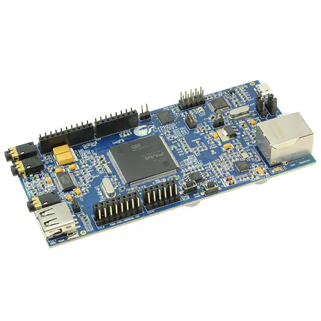


 工商网监
湘ICP备2023018690号
工商网监
湘ICP备2023018690号