STK15C88
256-Kbit (32 K × 8) PowerStore nvSRAM
Features
Functional Description
■
25 ns and 45 ns Access Times
The Cypress STK15C88 is a 256Kb fast static RAM with a
nonvolatile element in each memory cell. The embedded
nonvolatile elements incorporate QuantumTrap™ technology
producing the world’s most reliable nonvolatile memory. The
SRAM provides unlimited read and write cycles, while
independent, nonvolatile data resides in the highly reliable
QuantumTrap cell. Data transfers from the SRAM to the
nonvolatile elements (the STORE operation) takes place
automatically at power down. On power up, data is restored to
the SRAM (the RECALL operation) from the nonvolatile memory.
Both the STORE and RECALL operations are also available
under software control.
■
Pin compatible with Industry Standard SRAMs
■
Automatic Nonvolatile STORE on power loss
■
Nonvolatile STORE under Software Control
■
Automatic RECALL to SRAM on Power Up
■
Unlimited Read/Write Endurance
■
Unlimited RECALL Cycles
■
1,000,000 STORE Cycles
■
100 year Data Retention
■
Single 5 V + 10% Power Supply
■
Commercial and Industrial Temperatures
PowerStore nvSRAM products depend on the intrinsic system
capacitance to maintain system power long enough for an
automatic store on power loss. If the power ramp from 5 volts to
3.6 volts is faster than 10 ms, consider our 14C88 or 16C88 for
more reliable operation.
■
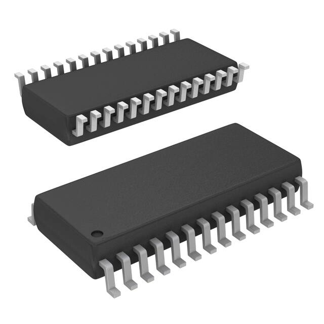
28-pin (300 mil and 330 mil) SOIC packages
For a complete list of related documentation, click here.
■
RoHS Compliance
Logic Block Diagram
Cypress Semiconductor Corporation
Document Number: 001-50593 Rev. *G
•
198 Champion Court
•
San Jose, CA 95134-1709
•
408-943-2600
Revised March 20, 2015
Not recommended for new designs. In production to support ongoing production programs only.
256-Kbit (32 K × 8) PowerStore nvSRAM
�STK15C88
Pin Configurations ...........................................................
Device Operation ..............................................................
SRAM Read .......................................................................
SRAM Write .......................................................................
AutoStore Operation ........................................................
Hardware RECALL (Power Up)........................................
Software STORE ...............................................................
Software RECALL.............................................................
Hardware Protect..............................................................
Noise Considerations.......................................................
Low Average Active Power..............................................
Best Practices...................................................................
Maximum Ratings.............................................................
DC Electrical Characteristics ..........................................
Data Retention and Endurance .......................................
Capacitance ......................................................................
Thermal Resistance..........................................................
AC Test Conditions ..........................................................
AC Switching Characteristics .........................................
SRAM Read Cycle.............................................................
Document Number: 001-50593 Rev. *G
3
4
4
4
4
4
4
4
5
5
5
5
7
7
8
8
8
8
9
9
Switching Waveforms ...................................................... 9
SRAM Write Cycle .......................................................... 10
Switching Waveforms .................................................... 10
AutoStore or Power Up RECALL .................................. 11
Switching Waveforms .................................................... 11
Software Controlled STORE/RECALL Cycle................ 12
Ordering Information...................................................... 13
Ordering Code Definitions ......................................... 13
Package Diagrams.......................................................... 14
Acronyms ........................................................................ 16
Document Conventions ................................................. 16
Units of Measure ....................................................... 16
Document History Page ................................................. 17
Sales, Solutions and Legal Information ....................... 18
Worldwide Sales and Design Support....................... 18
Products .................................................................... 18
PSoC® Solutions ...................................................... 18
Cypress Developer Community................................. 18
Technical Support ..................................................... 18
Page 2 of 18
Not recommended for new designs. In production to support ongoing production programs only.
Contents
�STK15C88
Pin Configurations
A14
1
28
VCC
A12
A7
2
27
3
26
WE
A13
A6
4
5
25
24
6
23
A5
A4
A3
7
(TOP)
22
A8
A9
A11
A2
8
21
OE
A10
A1
9
20
CE
A0
10
19
DQ7
DQ0
11
18
DQ6
DQ1
DQ2
12
17
VSS
13
16
DQ5
DQ4
14
15
DQ3
Table 1. Pin Definitions – 28-pin SOIC
Pin Name
Alt
I/O Type
A0–A14
Input
DQ0-DQ7
Input or
Output
Description
Address Inputs. Used to select one of the 32,768 bytes of the nvSRAM.
Bidirectional Data I/O lines. Used as input or output lines depending on operation.
WE
W
Input
Write Enable Input, Active LOW. When the chip is enabled and WE is LOW, data on the
I/O pins is written to the specific address location.
CE
E
Input
Chip Enable Input, Active LOW. When LOW, selects the chip. When HIGH, deselects the
chip.
OE
G
Input
Output Enable, Active LOW. The active LOW OE input enables the data output buffers
during read cycles. Deasserting OE HIGH causes the I/O pins to tristate.
VSS
VCC
Ground
Ground for the Device. The device is connected to ground of the system.
Power Supply Power Supply Inputs to the Device.
Document Number: 001-50593 Rev. *G
Page 3 of 18
Not recommended for new designs. In production to support ongoing production programs only.
Figure 1. Pin Diagram – 28-pin SOIC
�Device Operation
Software STORE
The STK15C88 is a versatile memory chip that provides several
modes of operation. The STK15C88 can operate as a standard
32 K × 8 SRAM. It has a 32 K × 8 nonvolatile element shadow to
which the SRAM information can be copied, or from which the
SRAM can be updated in nonvolatile mode.
Data is transferred from the SRAM to the nonvolatile memory by
a software address sequence. The STK15C88 software STORE
cycle is initiated by executing sequential CE controlled READ
cycles from six specific address locations in exact order. During
the STORE cycle, an erase of the previous nonvolatile data is
first performed, followed by a program of the nonvolatile
elements. When a STORE cycle is initiated, input and output are
disabled until the cycle is completed.
SRAM Read
The STK15C88 performs a READ cycle whenever CE and OE
are LOW while WE is HIGH. The address specified on pins A0–14
determines the 32,768 data bytes accessed. When the READ is
initiated by an address transition, the outputs are valid after a
delay of tAA (READ cycle 1). If the READ is initiated by CE or OE,
the outputs are valid at tACE or at tDOE, whichever is later (READ
cycle 2). The data outputs repeatedly respond to address
changes within the tAA access time without the need for transitions on any control input pins, and remains valid until another
address change or until CE or OE is brought HIGH.
SRAM Write
A WRITE cycle is performed whenever CE and WE are LOW.
The address inputs must be stable prior to entering the WRITE
cycle and must remain stable until either CE or WE goes HIGH
at the end of the cycle. The data on the common I/O pins DQ0–7
are written into the memory if it has valid tSD, before the end of
a WE controlled WRITE or before the end of an CE controlled
WRITE. Keep OE HIGH during the entire WRITE cycle to avoid
data bus contention on common I/O lines. If OE is left LOW,
internal circuitry turns off the output buffers tHZWE after WE goes
LOW.
AutoStore Operation
The STK15C88 uses the intrinsic system capacitance to perform
an automatic STORE on power down. As long as the system
power supply takes at least tSTORE to decay from VSWITCH down
to 3.6 V, the STK15C88 will safely and automatically store the
SRAM data in nonvolatile elements on power down.
In order to prevent unneeded STORE operations, automatic
STOREs will be ignored unless at least one WRITE operation
has taken place since the most recent STORE or RECALL cycle.
Software initiated STORE cycles are performed regardless of
whether a WRITE operation has taken place.
Hardware RECALL (Power Up)
During power up or after any low power condition (VCC <
VRESET), an internal RECALL request is latched. When VCC
once again exceeds the sense voltage of VSWITCH, a RECALL
cycle is automatically initiated and takes tHRECALL to complete.
If the STK15C88 is in a WRITE state at the end of power up
RECALL, the SRAM data is corrupted. To help avoid this
situation, a 10 Kohm resistor is connected either between WE
and system VCC or between CE and system VCC.
Document Number: 001-50593 Rev. *G
Because a sequence of READs from specific addresses is used
for STORE initiation, it is important that no other READ or WRITE
accesses intervene in the sequence. If they intervene, the
sequence is aborted and no STORE or RECALL takes place.
To initiate the software STORE cycle, the following READ
sequence is performed:
1. Read address 0x0E38, Valid READ
2. Read address 0x31C7, Valid READ
3. Read address 0x03E0, Valid READ
4. Read address 0x3C1F, Valid READ
5. Read address 0x303F, Valid READ
6. Read address 0x0FC0, Initiate STORE cycle
The software sequence is clocked with CE controlled READs.
When the sixth address in the sequence is entered, the STORE
cycle commences and the chip is disabled. It is important that
READ cycles and not WRITE cycles are used in the sequence.
It is not necessary that OE is LOW for a valid sequence. After the
tSTORE cycle time is fulfilled, the SRAM is again activated for
READ and WRITE operation.
Software RECALL
Data is transferred from the nonvolatile memory to the SRAM by
a software address sequence. A software RECALL cycle is
initiated with a sequence of READ operations in a manner similar
to the software STORE initiation. To initiate the RECALL cycle,
the following sequence of CE controlled READ operations is
performed:
1. Read address 0x0E38, Valid READ
2. Read address 0x31C7, Valid READ
3. Read address 0x03E0, Valid READ
4. Read address 0x3C1F, Valid READ
5. Read address 0x303F, Valid READ
6. Read address 0x0C63, Initiate RECALL cycle
Internally, RECALL is a two step procedure. First, the SRAM data
is cleared, and then the nonvolatile information is transferred into
the SRAM cells. After the tRECALL cycle time, the SRAM is once
again ready for READ and WRITE operations. The RECALL
operation does not alter the data in the nonvolatile elements. The
nonvolatile data can be recalled an unlimited number of times.
Page 4 of 18
Not recommended for new designs. In production to support ongoing production programs only.
STK15C88
�STK15C88
Figure 3. Current Versus Cycle Time (READ)
The STK15C88 offers hardware protection against inadvertent
STORE operation and SRAM WRITEs during low voltage
conditions. When VCC (VCC – 0.2 V). All other inputs cycling.
at tRC= 200 ns, 5 V, Dependent on output loading and cycle rate. Values obtained without
output loads.
25 °C Typical
–
10
mA
ICC4
Average Current
during AutoStore
Cycle
–
2
mA
ISB1[3]
Average VCC Current tRC = 25 ns, CE > VIH
tRC = 45 ns, CE > VIH
(Standby, Cycling
TTL Input Levels)
Commercial
–
30
22
mA
Industrial
–
31
23
mA
All Inputs Do Not Care, VCC = Max
Average current for duration tSTORE
ISB2[3]
VCC Standby Current CE > (VCC – 0.2 V). All others VIN < 0.2 V or > (VCC – 0.2 V).
(Standby, Stable
CMOS Input Levels)
–
1.5
mA
IIX
Input Leakage
Current
VCC = Max, VSS < VIN < VCC
–1
+1
A
IOZ
Off State Output
Leakage Current
VCC = Max, VSS < VIN < VCC, CE or OE > VIH or WE < VIL
–5
+5
A
VIH
Input HIGH Voltage
2.2
VCC +
0.5
V
VIL
Input LOW Voltage
VSS –
0.5
0.8
V
VOH
Output HIGH Voltage IOUT = –4 mA
2.4
–
V
VOL
Output LOW Voltage IOUT = 8 mA
–
0.4
V
Note
3. CE > VIH will not produce standby current levels until any nonvolatile cycle in progress has timed out.
Document Number: 001-50593 Rev. *G
Page 7 of 18
Not recommended for new designs. In production to support ongoing production programs only.
Exceeding maximum ratings may shorten the useful life of the
device. These user guidelines are not tested.
�STK15C88
Parameter
Description
DATAR
Data Retention
NVC
Nonvolatile STORE Operations
Min
Unit
100
Years
1,000
K
Capacitance
In the following table, the capacitance parameters are listed.[4]
Parameter
Description
CIN
Input Capacitance
COUT
Output Capacitance
Test Conditions
TA = 25 C, f = 1 MHz,
VCC = 0 to 3.0 V
Max
Unit
5
pF
7
pF
Thermal Resistance
In the following table, the thermal resistance parameters are listed.[4]
Parameter
Description
JA
Thermal Resistance
(Junction to Ambient)
JC
Thermal Resistance
(Junction to Case)
28-pin SOIC 28-pin SOIC
(300 mil)
(330 mil)
Test Conditions
Test conditions follow standard test methods and
procedures for measuring thermal impedance,
per EIA / JESD51.
Unit
TBD
TBD
C/W
TBD
TBD
C/W
Figure 4. AC Test Loads
R1 480
5.0 V
Output
30 pF
R2
255
AC Test Conditions
Input Pulse Levels .................................................. 0 V to 3 V
Input Rise and Fall Times (10% - 90%)........................ VIH; device is continuously selected.
7. Measured ±200 mV from steady state output voltage.
Document Number: 001-50593 Rev. *G
Page 9 of 18
Not recommended for new designs. In production to support ongoing production programs only.
SRAM Read Cycle
�STK15C88
SRAM Write Cycle
tWC
tPWE
tSCE
tSD
tHD
tAW
tSA
tHA
tHZWE [7,8]
tLZWE [7]
25 ns
Description
Alt
tAVAV
tWLWH, tWLEH
tELWH, tELEH
tDVWH, tDVEH
tWHDX, tEHDX
tAVWH, tAVEH
tAVWL, tAVEL
tWHAX, tEHAX
tWLQZ
tWHQX
Min
Write Cycle Time
Write Pulse Width
Chip Enable To End of Write
Data Setup to End of Write
Data Hold After End of Write
Address Setup to End of Write
Address Setup to Start of Write
Address Hold After End of Write
Write Enable to Output Disable
Output Active After End of Write
45 ns
Max
25
20
20
10
0
20
0
0
Min
Max
45
30
30
15
0
30
0
0
10
5
15
5
Unit
ns
ns
ns
ns
ns
ns
ns
ns
ns
ns
Switching Waveforms
Figure 7. SRAM Write Cycle 1: WE Controlled [8]
tWC
ADDRESS
tHA
tSCE
CE
tAW
tSA
tPWE
WE
tSD
tHD
DATA VALID
DATA IN
tHZWE
DATA OUT
tLZWE
HIGH IMPEDANCE
PREVIOUS DATA
Figure 8. SRAM Write Cycle 2: CE Controlled [8]
tWC
ADDRESS
CE
WE
tHA
tSCE
tSA
tAW
tPWE
tSD
DATA IN
DATA OUT
tHD
DATA VALID
HIGH IMPEDANCE
Notes
8. If WE is Low when CE goes Low, the outputs remain in the high impedance state.
9. CE or WE must be greater than VIH during address transitions.
Document Number: 001-50593 Rev. *G
Page 10 of 18
Not recommended for new designs. In production to support ongoing production programs only.
Parameter
Cypress
Parameter
�STK15C88
AutoStore or Power Up RECALL
tHRECALL [10]
tSTORE [6]
VRESET
VSWITCH
Alt
tRESTORE
tHLHZ
Description
Power up RECALL Duration
STORE Cycle Duration
Low Voltage Reset Level
Low Voltage Trigger Level
STK15C88
Min
Max
550
10
3.6
4.0
4.5
Unit
s
ms
V
V
Switching Waveforms
Figure 9. AutoStore/Power Up RECALL
VCC
5V
VSWITCH
VRESET
AutoStore™
tSTORE
POWER-UP RECALL
WE
tHRECALL
DQ (DATA OUT)
POWER-UP
RECALL
BROWN OUT
NO STORE DUE TO
NO SRAM WRITES
BROWN OUT
AutoStore
BROWN OUT
AutoStore
NO RECALL
(VCC DID NOT GO
BELOW VRESET)
NO RECALL
(VCC DID NOT GO
BELOW VRESET)
RECALL WHEN
VCC RETURNS
ABOVE VSWITCH
Note
10. tHRECALL starts from the time VCC rises above VSWITCH.
Document Number: 001-50593 Rev. *G
Page 11 of 18
Not recommended for new designs. In production to support ongoing production programs only.
Parameter
�STK15C88
Software Controlled STORE/RECALL Cycle
Parameter
Alt
25 ns
Description
Min
45 ns
Max
Min
Max
Unit
tRC
tAVAV
STORE/RECALL Initiation Cycle Time
25
45
ns
tSA[11]
tCW[11]
tHACE[7, 11]
tAVEL
Address Setup Time
0
0
ns
tELEH
Clock Pulse Width
20
30
ns
tELAX
Address Hold Time
20
20
ns
RECALL Duration
tRECALL
20
20
s
Switching Waveforms
Figure 10. CE Controlled Software STORE/RECALL Cycle [12]
tRC
ADDRESS # 1
ADDRESS
tSA
tRC
ADDRESS # 6
tSCE
CE
tHACE
OE
t STORE / t RECALL
DQ (DATA)
DATA VALID
DATA VALID
HIGH IMPEDANCE
Notes
11. The software sequence is clocked on the falling edge of CE without involving OE (double clocking will abort the sequence).
12. The six consecutive addresses must be read in the order listed in the Mode Selection table. WE must be HIGH during all six consecutive cycles.
Document Number: 001-50593 Rev. *G
Page 12 of 18
Not recommended for new designs. In production to support ongoing production programs only.
The software controlled STORE/RECALL cycle follows. [11, 12]
�STK15C88
Ordering Information
Speed
(ns)
25
45
Ordering Code
Package Diagram
Package Type
STK15C88-NF25ITR
51-85026
28-pin SOIC (300 mil)
STK15C88-NF25I
51-85026
28-pin SOIC (300 mil)
STK15C88-SF25ITR
51-85058
28-pin SOIC (330 mil)
STK15C88-SF25I
51-85058
28-pin SOIC (330 mil)
STK15C88-NF45TR
51-85026
28-pin SOIC (300 mil)
STK15C88-NF45
51-85026
28-pin SOIC (300 mil)
STK15C88-NF45ITR
51-85026
28-pin SOIC (300 mil)
STK15C88-NF45I
51-85026
28-pin SOIC (300 mil)
STK15C88-SF45ITR
51-85058
28-pin SOIC (330 mil)
STK15C88-SF45I
51-85058
28-pin SOIC (330 mil)
Operating Range
Industrial
Commercial
Industrial
All parts are Pb-free. The above table contains Final information. Contact your local Cypress sales representative for availability of these parts
Ordering Code Definitions
STK15C88 - N F 45 I TR
Packaging Option:
TR = Tape and Reel
Blank = Tube
Temperature Range:
Blank - Commercial (0 to 70°C)
I - Industrial (-40 to 85°C)
Speed:
25 - 25 ns
45 - 45 ns
Lead Finish
F = 100% Sn (Matte Tin)
Package:
N = Plastic 28-pin 300 mil SOIC
S = Plastic 28-pin 330 mil SOIC
Document Number: 001-50593 Rev. *G
Page 13 of 18
Not recommended for new designs. In production to support ongoing production programs only.
These parts are not recommended for new designs. They are in production to support ongoing production programs only.
�STK15C88
Package Diagrams
Not recommended for new designs. In production to support ongoing production programs only.
Figure 11. 28-pin (300 mil) SOIC, 51-85026
51-85026 *H
Document Number: 001-50593 Rev. *G
Page 14 of 18
�STK15C88
Package Diagrams (continued)
51-85058 *D
Document Number: 001-50593 Rev. *G
Page 15 of 18
Not recommended for new designs. In production to support ongoing production programs only.
Figure 12. 28-pin (330 mil) SOIC, 51-85058
�STK15C88
Acronym
CE
CMOS
Document Conventions
Description
Units of Measure
chip enable
Symbol
Unit of Measure
complementary metal oxide semiconductor
°C
degree Celsius
EIA
electronic industries alliance
Hz
hertz
I/O
input/output
kHz
kilohertz
nvSRAM
non-volatile static random access memory
k
kilo-ohm
OE
RoHS
output enable
MHz
megahertz
A
microampere
SRAM
static random access memory
F
microfarad
WE
write enable
s
microsecond
mA
milliampere
ms
millisecond
ns
nanosecond
ohm
%
percent
pF
picofarad
V
volt
W
watt
restriction of hazardous substances
Document Number: 001-50593 Rev. *G
Not recommended for new designs. In production to support ongoing production programs only.
Acronyms
Page 16 of 18
�STK15C88
Document Title: STK15C88 256-Kbit (32 K × 8) PowerStore nvSRAM
Document Number: 001-50593
Orig. of Submission
Change
Date
Revision
ECN
**
2625096
GVCH /
PYRS
12/19/08
*A
2826441
GVCH
12/11/2009
*B
3052511
GVCH
10/08/10
*C
3221180
GVCH
04/10/2011
Updated Package Diagrams.
Updated in new template.
*D
3527659
GVCH
02/17/2012
Package Diagrams: Updated 28-Pin (330 Mil) SOIC package diagram
*E
4306736
GVCH
03/13/2014
Typo fixed (Hardware Protect): Changed VCAP < VSWITCH to VCC < VSWITCH
Updated Package Diagrams:
spec 51-85026 – Changed revision from *F to *H.
Updated in new template.
*F
4568935
GVCH
11/14/2014
Added documentation related hyperlink in page 1
Identified all parts under ‘Not recommended for New Design’
*G
4693449
GVCH
03/20/2015
Updated package diagram spec 51-85058 *C to 51-85058 *D
Document Number: 001-50593 Rev. *G
Description of Change
New data sheet
Added following text in the Ordering Information section: “These parts are not
recommended for new designs. In production to support ongoing production
programs only.”
Added watermark in PDF stating “Not recommended for new designs. In
production to support ongoing production programs only.”
Added Contents on page 2.
Removed the following inactive parts from the Ordering Information table:
STK15C88-NF25, STK15C88-NF25TR, STK15C88-SF25, STK15C88-SF25TR,
STK15C88-SF45, STK15C88-SF45TR
Updated package diagrams
Page 17 of 18
Not recommended for new designs. In production to support ongoing production programs only.
Document History Page
�STK15C88
Sales, Solutions and Legal Information
Cypress maintains a worldwide network of offices, solution centers, manufacturer’s representatives, and distributors. To find the office
closest to you, visit us at Cypress Locations.
PSoC® Solutions
Products
Automotive
Clocks & Buffers
Interface
Lighting & Power Control
cypress.com/go/automotive
cypress.com/go/clocks
cypress.com/go/interface
cypress.com/go/powerpsoc
cypress.com/go/plc
Memory
PSoC
Touch Sensing
USB Controllers
Wireless/RF
cypress.com/go/memory
cypress.com/go/psoc
psoc.cypress.com/solutions
PSoC 1 | PSoC 3 | PSoC 4 | PSoC 5LP
Cypress Developer Community
Community | Forums | Blogs | Video | Training
Technical Support
cypress.com/go/support
cypress.com/go/touch
cypress.com/go/USB
cypress.com/go/wireless
© Cypress Semiconductor Corporation, 2009-2015. The information contained herein is subject to change without notice. Cypress Semiconductor Corporation assumes no responsibility for the use of
any circuitry other than circuitry embodied in a Cypress product. Nor does it convey or imply any license under patent or other rights. Cypress products are not warranted nor intended to be used for
medical, life support, life saving, critical control or safety applications, unless pursuant to an express written agreement with Cypress. Furthermore, Cypress does not authorize its products for use as
critical components in life-support systems where a malfunction or failure may reasonably be expected to result in significant injury to the user. The inclusion of Cypress products in life-support systems
application implies that the manufacturer assumes all risk of such use and in doing so indemnifies Cypress against all charges.
Any Source Code (software and/or firmware) is owned by Cypress Semiconductor Corporation (Cypress) and is protected by and subject to worldwide patent protection (United States and foreign),
United States copyright laws and international treaty provisions. Cypress hereby grants to licensee a personal, non-exclusive, non-transferable license to copy, use, modify, create derivative works of,
and compile the Cypress Source Code and derivative works for the sole purpose of creating custom software and or firmware in support of licensee product to be used only in conjunction with a Cypress
integrated circuit as specified in the applicable agreement. Any reproduction, modification, translation, compilation, or representation of this Source Code except as specified above is prohibited without
the express written permission of Cypress.
Disclaimer: CYPRESS MAKES NO WARRANTY OF ANY KIND, EXPRESS OR IMPLIED, WITH REGARD TO THIS MATERIAL, INCLUDING, BUT NOT LIMITED TO, THE IMPLIED WARRANTIES
OF MERCHANTABILITY AND FITNESS FOR A PARTICULAR PURPOSE. Cypress reserves the right to make changes without further notice to the materials described herein. Cypress does not
assume any liability arising out of the application or use of any product or circuit described herein. Cypress does not authorize its products for use as critical components in life-support systems where
a malfunction or failure may reasonably be expected to result in significant injury to the user. The inclusion of Cypress’ product in a life-support systems application implies that the manufacturer
assumes all risk of such use and in doing so indemnifies Cypress against all charges.
Use may be limited by and subject to the applicable Cypress software license agreement.
Document Number: 001-50593 Rev. *G
Revised March 20, 2015
All products and company names mentioned in this document may be the trademarks of their respective holders.
Page 18 of 18
Not recommended for new designs. In production to support ongoing production programs only.
Worldwide Sales and Design Support
�


 工商网监
湘ICP备2023018690号
工商网监
湘ICP备2023018690号
