DS1085L
3.3V EconOscillator Frequency
Synthesizer
www.maxim-ic.com
FEATURES
§
§
§
§
§
§
§
§
§
§
§
§
User-Programmable Frequency Synthesizer
Programmable From 4.1kHz to 66MHz
Dual Synchronous Outputs
4.13MHz to 66MHz Reference Oscillator
Output
4.1kHz to 66MHz Main Oscillator Output
Single 3.0 to 3.6V Supply
Three Resolution Options
2-Wire Serial Interface
0.75% Absolute Accuracy
Nonvolatile (NV) Frequency Settings
No External Timing Components
Power-Down Mode
OUT1
1
8
SCL
OUT0
2
7
SDA
VCC
3
CTRL1
GND
4
6
5
CTRL0
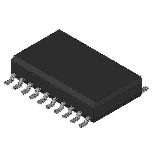
SO (150mil)
PIN DESCRIPTION
OUT1
- Main Oscillator Output
OUT0
- Reference Oscillator Output
- Power-Supply Voltage
VCC
GND
- Ground
CTRL1 - Control Pin for OUT1
CTRL0 - Control Pin for OUT0
SDA
- 2-Wire Serial Data Input/Output
SCL - 2-Wire Serial Clock
ORDERING INFORMATION
PIN ASSIGNMENT
DS1085LZ-5
150mil SO
STEP
SIZE
5kHz
DS1085LZ-12
150mil SO
12.5kHz
4.1kHz to 66MHz
DS1085LZ-25
150mil SO
25kHz
4.1kHz to 66MHz
DEVICE
PACKAGE
OSCILLATOR
OUTPUT RANGE
4.1kHz to 66MHz
DESCRIPTION
The DS1085L is a dual-output frequency synthesizer requiring no external timing components for
operation. It can be used as a standalone oscillator or as a dynamically programmed, processor-controlled
peripheral device. An internal master oscillator can be programmed from 33MHz to 66MHz with three
resolution options of 5kHz, 12.5kHz, and 25kHz. A programmable 3-bit prescaler (divide-by-1, 2, 4, or 8)
permits the generation of a reference oscillator output (OUT0) from the master, ranging from 4.13MHz to
66MHz. A second independent prescaler and a 1-to-1025 divider allow the generation of a main oscillator
output (OUT1) from 4.1kHz to 66MHz. The two outputs, although synchronous with the master, can be
independently programmed. The combination of programmable master oscillator, prescalers, and dividers
allows the generation of thousands of user-specified frequencies. All master oscillator, prescaler, and
divider settings are stored in NV (EEPROM) memory, providing a default value on power-up that allows
it to be used as a standalone oscillator. A 2-wire serial interface allows in-circuit, on-the-fly programming
of the master oscillator, prescalers (P0 and P1), and divider (N). This allows dynamic frequency
modification, if required, or, for fixed-frequency applications, the DS1085L can be used with factory- or
user-programmed values.
EconOscillator is a trademark of Dallas Semiconductor.
1 of 21
051606
�DS1085L
External control inputs, CTRL1 and CTRL0, enable or disable the two oscillator outputs. Both outputs
feature a synchronous enable that ensures no output glitches when the output is enabled and a constant
time interval (for a given frequency setting) from an enable signal to the first output transition. These
inputs can also be configured to disable the master oscillator, putting the device into a low-power mode
for power-sensitive applications.
Figure 1. DS1085L BLOCK DIAGRAM
0M0
0M1
1M0
1M1
OVERVIEW
A block diagram of the DS1085L is shown in Figure 1. The DS1085L consists of five major components:
§
§
§
§
§
Internal master oscillator (33MHz to 66MHz)
Master oscillator control DAC
Prescalers (divide-by-1, 2, 4, or 8)
Programmable divider (divide-by-1 to 1025)
Control registers
The internal master oscillator provides the reference clock (MCLK), which is fed to the prescalers and
programmable dividers. The frequency of the oscillator can be user-programmed over a two-to-one range
in increments equal to the step size, by means of a 10-bit control DAC. The master oscillator range is
33MHz to 66MHz, which is larger than the range possible with the 10-bit DAC resolution and available
step sizes. Therefore, an additional register (OFFSET) is provided that can be used to select the range of
frequency over which the DAC is used (see Table 1).
2 of 21
�DS1085L
Table 1. DEVICE COMPARISONS BY PART NUMBER
PART NUMBER
STEP SIZE (kHz)
DAC SPAN (MHz)
OFFSET SIZE (MHz)
DS1085LZ-5
5
5.12
2.56
DS1085LZ-12
12.5
12.80
3.20
DS1085LZ-25
25
25.60
3.20
For further description of use of the OFFSET register see the REGISTER FUNCTIONS section.
The master clock can be routed directly to the outputs (OUT0 and OUT1) or through separate prescalers
(P0 and P1). In the case of OUT1, an additional programmable divider (N) can be used to generate
frequencies down to 4.1kHz.
The prescaler (P0) divides MCLK by 1, 2, 4, or 8 before routing MCLK to the reference output (OUT0)
pin.
The prescaler (P1) divides MCLK by 1, 2, 4, or 8 before routing MCLK to the programmable divider (N),
and ultimately to the main output (OUT1) pin.
The programmable divider (N) divides the prescaler output (P1) by any number selected between two and
1025 (10 bits) to provide the main output (OUT1), or it can be bypassed altogether by use of the DIV1
register bit. The value of N is stored in the DIV register.
The control registers are user-programmable through a 2-wire serial interface to determine operating
frequency (values of DAC, OFFSET, P0, P1, and N) and modes of operation. Once programmed, the
register settings are nonvolatile and only need reprogramming if it is desired to reconfigure the device.
PIN DESCRIPTIONS
PIN
NAME
1
OUT1
2
OUT0
3
4
Vcc
GND
5
CTRL0
6
CTRL1
7
SDA
8
SCL
FUNCTION
This main oscillator output frequency is determined by the control
register settings for the oscillator (DAC and OFFSET), prescaler P1
(mode bits 1M0 and 1M1), and divider N (DIV).
The reference output is taken from the output of the reference select mux.
Its frequency is determined by the control register settings for prescaler
P0 (mode bits 0M0 and 0M1) (see Table 2).
Power Supply
Ground
A multifunction control input pin that can be programmed to function as
a mux select, ouput enable, and/or a power-down. Its function is
determined by the user-programmable control register values of EN0,
SEL0, and PDN0 (see Table 2).
A multifunction control input pin that can be programmed to function as
an output enable and/or a power-down. Its function is determined by the
user-programmable control register value of PDN1 (see Table 3).
I/O pin for the 2-wire serial interface used for data transfer.
Input pin for the 2-wire serial interface used to synchronize data
movement over the serial interface.
3 of 21
�DS1085L
Table 2. DEVICE MODE USING OUT0
EN0
(BIT)
SEL0
(BIT)
PDN0
(BIT)
CTRL0
OUT0
CTRL0
DEVICE
(PIN)
(PIN)
FUNCTION
MODE
1
High-Z
Power-Down*
Power-Down***
0
0
0
0
High-Z
Active
Mux Select
1
MCLK/M
0
1
0
Active
0
MCLK
Output Enable
1
High-Z
1
0
0
Active
0
MCLK
1
High-Z
Output Enable
1
1
0
Active**
0
MCLK/M
Power-Down
1
High-Z
Power-Down
X
0
1
0
MCLK
Active
1
High-Z
Power-Down
Power-Down
X
1
1
0
MCLK/M
Active
* This mode is for applications where OUT0 is not used, but CTRL0 is used as a device shutdown.
** Factory default setting.
***See standby (power-down) current specification for power-down current range.
Table 3. DEVICE MODE USING OUT1
PDN1
CTRL1
(BIT)
(PIN)
0
0
0
1
1
0
1
1
*Factory default setting
CTRL1
FUNCTION
Output Enable
Power-Down
OUT1 (PIN)
OUT CLK
High-Z
OUT CLK
High-Z
DEVICE MODE
Active*
Active
Power-Down
NOTE:
Both CTRL0 and CTRL1 can be configured as power-downs. They are internally “OR” connected so
either of the control pins can be used to provide a power-down function for the whole device, subject to
appropriate settings of the PDN0 and PDN1 register bits (see Table 4).
Table 4. SHUTDOWN CONTROL WITH PDN0 AND PDN1
PDN0
(BIT)
0
0
1
1
PDN1
(BIT)
0
1
0
1
SHUTDOWN CONTROL
NONE
CTRL1
CTRL0
CTRL1 OR CTRL0
4 of 21
�DS1085L
REGISTER FUNCTIONS
The user-programmable registers can be used to determine the mode of operation (MUX), operating
frequency (DAC, OFFSET, DIV), and bus settings (ADDR). The functions of the registers are described
in this section, but the details of how these registers are programmed can be found in a later section. The
register settings are nonvolatile, with the values being stored automatically or as required in EEPROM
when the registers are programmed through the SDA and SCL pins.
DAC WORD (Address 08h)
MSB
d9
d8
d7
d6
d5
d4
First Data Byte
d3
LSB
d2
MSB
d1
d0
X
X
X
X
Second Data Byte
LSB
X
X
X = Don’t care.
The DAC word (d0–d9) controls the frequency of the master oscillator. The resolution of this register
depends on the step size of the device. The absolute frequency of the device also depends on the value of
the OFFSET register (see Tables 5 and 6).
Table 5. DEVICE DEFAULT SETTINGS
DS1085LZ-5
Frequency
48.58MHz
DAC
500
Offset
OS
DS1085LZ-12
Frequency
DAC Offset
52.3MHz
600
OS
DS1085LZ-25
Frequency
DAC
50.9MHz
500
Offset
OS
For any given value of OFFSET the master oscillator frequency can be derived as follows:
Frequency = Min Frequency + DAC x Step Size
where: Min frequency is the lowest frequency shown in Table 6 for the corresponding offset.
DAC is the value of the DAC register (0–1023).
Step size is the step size of the device (5kHz, 12.5kHz, or 25kHz).
OS is the decimal, integer value of the 5 MSBs of the RANGE register.
OFFSET BYTE (Address
MSB
X
X
X = Don’t care.
0Eh)
X
O4
O3
O2
O1
LSB
O0
The OFFSET byte (O0–O4) determines the range of frequencies that can be obtained within the absolute
minimum and maximum range of the oscillator. Correct operation of the device is not guaranteed for
values of OFFSET not shown in Table 6.
5 of 21
�DS1085L
Table 6. FREQUENCY vs. OFFSET
OFFSET
OS - 10
OS - 9
OS - 8
OS - 7
OS - 6
OS - 5
OS - 4
OS - 3
OS - 2
OS - 1
OS*
OS + 1
OS + 2
OS + 3
OS + 4
OS + 5
OS + 6
DS1085LZ-5
FREQUENCY
RANGE
—
—
—
—
30.7 to 35.8
33.3 to 38.4
35.8 to 41.0
38.4 to 43.5
41.0 to 46.1
43.5 to 48.6
46.1 to 51.2
48.6 to 53.8
51.2 to 56.3
53.8 to 58.9
56.3 to 61.4
58.9 to 64.0
61.4 to 66.6
DS1085LZ-12
FREQUENCY
RANGE
—
—
—
—
25.6 to 38.4
28.8 to 41.6
32.0 to 44.8
35.2 to 48.0
38.4 to 51.2
41.6 to 54.4
44.8 to 57.6
48.0 to 60.8
51.2 to 64.0
54.4 to 67.2
57.6 to 70.4
60.8 to 73.6
64.0 to 76.8
DS1085LZ-25
FREQUENCY
RANGE
—
—
—
—
19.2 to 44.8
22.4 to 48.0
25.6 to 51.2
28.8 to 54.4
32.0 to 57.6
35.2 to 60.8
38.4 to 64.0
41.6 to 67.2
44.8 to 70.4
48.0 to 73.6
51.2 to 76.8
54.4 to 80.0
57.6 to 83.2
*OS is the OFFSET default setting. OS is the integer value of the five MSBs of RANGE register.
These ranges include values outside the oscillator range of 33MHz to 66MHz. When using these ranges,
values of DAC must be chosen to keep the oscillator within range. Correct operation of the device is not
guaranteed outside the range 33MHz to 66MHz.
MUX WORD (Address 02h)
The MUX word controls several functions. Its bits are organized as follows:
MSB
LSB MSB
NAME * PDN1 PDN0 SEL0 EN0 0M1 0M0 1M1 1M0
Default
0
0
0
1
1
0
0
0
0
Setting
* This bit must be set to zero.
X = Don’t care.
6 of 21
LSB
DIV1 – – – – – –
0
X X X X X X
�DS1085L
The functions of the individual bits are described in the following paragraphs.
DIV1 (Default Setting = 0)
This bit allows the output of the prescaler P1 to be routed directly to the
OUT1 pin (DIV1 = 1). In this condition, the N divider is bypassed so the
programmed value of N is ignored. If DIV1 = 0, the N divider functions
normally.
EN0 (Default Setting = 1)
If EN0 = 1 and PDN0 = 0, the CTRL0 functions as an output enable for OUT0, the frequency of the
output being determined by the SEL0 bit.
If PDN0 = 1, the EN0 bit is ignored, CTRL0 functions as a power-down, and OUT0 is always enabled on
power-up, its frequency determined by the SEL0 bit.
If EN0 = 0, the function of CTRL0 is determined by the SEL0 and PDN0 bits (see Table 2).
SEL0 (Default Setting = 1)
If SEL0 = 1 and EN0 = PDN0 = 0, the CTRL0 pin determines whether the prescaler is bypassed,
controlling the output frequency.
If CTRL0 = 0, the output frequency equals MCLK.
If CTRL0 = 1, the output frequency equals MCLK/M.
If either EN0 or PDN0 = 1, the CTRL0 pin functions as an output enable or power-down and the SEL0
bit determines whether the prescaler is bypassed, thus controlling the output frequency.
If SEL0 = 0, the output is MCLK, the master clock frequency.
If SEL0 = 1, the output is the output frequency of the M prescaler (see Table 2).
PDN0 (Default Setting = 0)
If PDN0 = 1, the CTRL0 performs a power-down function, regardless of the setting of the other bits.
If PDN0 = 0, the function of CTRL0 is determined by the values of EN0 and SEL0 (see Table 2).
0M0, 0M1, 1M0, 1M1 (Default Setting = 0)
These bits set the prescaler’s (P0 and P1) divisor (M) to 1, 2, 4, or 8 (see Table 7a and 7b).
7 of 21
�DS1085L
Table 7a. PRESCALER P0 DIVISOR M SETTINGS
0M1
0M0
PRESCALER P0
DIVISOR “M”
0
0
1*
0
1
2
1
0
4
1
1
8
*Factory Default Setting
Table 7b. PRESCALER P1 DIVISOR M SETTINGS
1M1
1M0
PRESCALER P1
DIVISOR “M”
0
0
1*
0
1
2
1
0
4
1
1
8
*Factory Default Setting
NOTE:
When EN0 = SEL0 = PDN0 = 0, CTRL0 also functions as a power-down. This is a special case for
situations when OUT0 is not used. Under these conditions all the circuitry associated with OUT0 is
powered down. OUT0 is powered down (see Table 2).
PDN1 (Default Setting = 0)
If PDN1 = 1, CTRL1 functions as a power-down (see Table 3).
·
If PDN1 = 0, CTRL1 functions as an output enable for OUT1 (see Table 3).
NOTES FOR OUTPUT ENABLE AND POWER-DOWN:
1)
2)
3)
4)
5)
Both enables are “smart” and wait for the output to be low before going High-Z.
A power-down sequence first disables both outputs before powering down the device.
On power-up, the outputs are disabled until the clock has stabilized (~8000 cycles).
In power-down mode the device cannot be programmed.
A power-down command must persist for at least two cycles of the lowest output frequency plus
10µs.
DIV WORD (N) (Address 01h)
MSB
N9 N8
N7
N6 N5 N4
First Data Byte
LSB
N3 N2
MSB
N1 N0
X = Don’t care.
8 of 21
X
X
X
X
Second Data Byte
X
LSB
X
�DS1085L
N
The DIV word sets the programmable divider. These 10 bits (N0–N9) determine the value of the
programmable divider (N). The range of divisor values is from two to 1025, and is equal to the
programmed value of N plus 2 (see Table 8).
Table 8. PROGRAMMABLE DIVISOR N VALUES
BIT VALUE
00000000 00XXXXXX
00000000 01XXXXXX
—
—
—
—
11111111 11XXXXXX
* Factory Default Setting
DIVISOR (N)
2*
3
—
—
—
—
1025
ADDR BYTE (Address 0Dh)
MSB
—
X
NAME
Factory
Default
X = Don’t care.
—
X
—
X
—
X
WC
0
A2
0
A1
0
LSB
A0
0
A0, A1, A2 (Default Setting = 000)
These device select bits determine the 2-wire address of the device.
WC (Default Setting = 0)
This bit determines when/if the EEPROM is written to after register contents have been changed. If
WC = 0, EEPROM is written automatically after a write register command. If WC = 1, EEPROM is only
written when the “WRITE” command is issued. In applications where the register contents are frequently
rewritten, WC should be set to 1; otherwise, it is necessary to wait for an EEPROM write cycle to
complete (up to 10ms) between writing to the registers. Regardless of the value of the WC bit, when the
ADDR register (A0, A1, A2) is written, the current value in all registers (DAC, OFFSET, DIV, MUX,
and ADDR) are immediately to the EEPROM.
RANGE REGISTER (Address 37h)
MSB
OS5 OS4
OS3
OS2
OS1
X
X
X
X
X
X
X
X
X
X
The first five bits of the RANGE register contain the default OFFSET value. The decimal value of the
RANGE register is the value OS that is referred to in Table 6. The RANGE register is read-only.
9 of 21
LSB
X
�DS1085L
COMMAND SET
Data and control information is read from and written to the DS1085L in the format shown in Figure 3.
To write to the DS1085L, the master issues the slave address of the DS1085L and the R/ W bit is set to 0.
After receiving an acknowledge, the bus master provides a command protocol. After receiving this
protocol, the DS1085L issues an acknowledge, and then the master can send data to the DS1085L. If the
DS1085L is to be read, the master must send the command protocol as before, and then issue a repeat
START condition and then the control byte again, this time with the R/ W bit set to 1 to allow reading of
the data from the DS1085L. The command set for the DS1085L is listed as follows:
Access DAC [08h]
If R/ W is 0, this command writes to the DAC register. After issuing this command, the next data byte
values are written into the DAC register. If R/ W is 1, the next data bytes read are the values stored in the
DAC register. This is a 2-byte transfer, the first byte contains the eight MSBs, and the second byte
contains the two LSBs in the most significant positions of the data byte. The remaining six bits are
ignored and can be written with any value (if read, these bits are 0).
Access OFFSET [0Eh]
If R/ W is 0, this command writes to the OFFSET register. After issuing this command, the next data byte
value is written into the OFFSET register. If R/ W is 1, the next data byte read is the value stored in the
OFFSET register. This is a single-byte transfer of which only the five LSBs (last five bits) are used. The
remaining three bits can be written with any value to complete the data byte (if read, these bits are 1).
Access DIV [01h]
If R/ W is 0, this command writes to the DIV register. After issuing this command, the next data byte
values are written into the DIV register. If R/ W is 1, the next data bytes read are the values stored in the
DIV register. This register has a 10-bit value. The upper eight bits are sent first, followed by a second
byte that contains the two LSBs of the register value in the most significant positions of the data byte.
The remaining six bits are ignored and can be set to any value (if read, these bits are 0).
Access MUX [02h]
If R/ W is 0, this command writes to the MUX register. After issuing this command, the next data byte
values are written into the MUX register. If R/ W is 1, the next data bytes read are the values stored in the
MUX register. This register has a 10-bit value. The upper eight bits are sent first, followed by a second
byte that contains the two LSBs of the register value in the most significant positions of the data byte.
The remaining six bits are ignored and can be set to any value (if read, these bits are 0).
Access ADDR [0Dh]
If R/ W is 0, this command writes to the ADDR register. After issuing this command, the next data byte
value is written into the ADDR register. If R/ W is 1, the next data byte read is the value stored in the
ADDR register. This is a single-byte transfer. This register has a 5-bit value, the first three bits of a write
can be any value followed by the five active bits (if read, the first three bits are 0).
10 of 21
�DS1085L
Access RANGE [37h]
If R/ W is 1, the next data bytes read are the values stored in the RANGE register. This register has a 14bit value. The upper eight bits are sent first, followed by a second byte that contains the five LSBs of the
register value in the most significant positions of the data byte. The upper five MSB’s of the first byte
contain the OS value for the frequency adjust Table 6. The register is read-only.
Write E2 [3Fh]
If WC = 0, the EEPROM is automatically written to at the end of each write command. This is a
DEFAULT condition. In this case the command “WRITE E2” is not needed. If WC = 1, the EEPROM is
written when the “WRITE E2” command is issued. On receipt of the “WRITE E2” command, the
contents of the DAC, OFFSET, ADDR, DIV and MUX registers are written into the EEPROM, thus
locking in the register settings.
EXCEPTION: The DAC, OFFSET, ADDR, DIV, and MUX registers are always automatically written to
EEPROM after a write to the ADDR register regardless of the value of the WC bit.
11 of 21
�DS1085L
2-WIRE SERIAL DATA BUS
The DS1085L communicates through a 2-wire serial interface. A device that sends data onto the bus is
defined as a transmitter, and a device receiving data as a receiver. The device that controls the message is
called a “master.” The devices that are controlled by the master are “slaves.” A master device that
generates the serial clock (SCL), controls the bus access, and generates the START and STOP conditions
must control the bus. The DS1085L operates as a slave on the 2–wire bus. Connections to the bus are
made through the open-drain I/O lines SDA and SCL.
The following bus protocol has been defined (see Figure 2):
§
§
Data transfer can be initiated only when the bus is not busy.
During data transfer, the data line must remain stable whenever the clock line is HIGH. Changes in
the data line while the clock line is high are interpreted as control signals.
Accordingly, the following bus conditions have been defined:
Bus not busy: Both data and clock lines remain HIGH.
Start data transfer: A change in the state of the data line, from HIGH to LOW, while the clock is
HIGH, defines a START condition.
Stop data transfer: A change in the state of the data line, from LOW to HIGH, while the clock line is
HIGH, defines the STOP condition.
Data valid: The state of the data line represents valid data when, after a START condition, the data line
is stable for the duration of the HIGH period of the clock signal. The data on the line must be changed
during the LOW period of the clock signal. There is one clock pulse per bit of data.
Each data transfer is initiated with a START condition and terminated with a STOP condition. The
number of data bytes transferred between START and STOP conditions is not limited, and is determined
by the master device. The information is transferred byte-wise and each receiver acknowledges with a
ninth bit.
Within the bus specifications a regular mode (100kHz clock rate) and a fast mode (400kHz clock rate) are
defined. The DS1085L works in both modes.
Acknowledge: Each receiving device, when addressed, is obliged to generate an acknowledge after the
byte has been received. The master device must generate an extra clock pulse that is associated with this
acknowledge bit.
A device that acknowledges must pull down the SDA line during the acknowledge clock pulse in such a
way that the SDA line is stable LOW during the HIGH period of the acknowledge-related clock pulse. Of
course, setup and hold times must be taken into account. When the DS1085L EEPROM is being written
to, it is not able to perform additional responses. In this case, the slave DS1085L sends a not acknowledge
to any data transfer request made by the master. It resumes normal operation when the EEPROM
operation is complete.
12 of 21
�DS1085L
A master must signal an end of data to the slave by not generating an acknowledge bit on the last byte
that has been clocked out of the slave. In this case, the slave must leave the data line HIGH to enable the
master to generate the STOP condition.
Figure 2. DATA TRANSFER ON 2-WIRE SERIAL BUS
Figures 2, 3, and 4 detail how data transfer is accomplished on the 2-wire bus. Depending upon the state
of the R/W bit, two types of data transfer are possible:
1) Data transfer from a master transmitter to a slave receiver. The first byte transmitted by the
master is the slave address. Next follows a number of data bytes. The slave returns an acknowledge
bit after each received byte.
2) Data transfer from a slave transmitter to a master receiver. The first byte (the slave address) is
transmitted by the master. The slave then returns an acknowledge bit. Next follows a number of data
bytes transmitted by the slave to the master. The master returns an acknowledge bit after all received
bytes other than the last byte. At the end of the last received byte, a not acknowledge is returned.
The master device generates all of the serial clock pulses and the START and STOP conditions. A
transfer is ended with a STOP condition or with a repeated START condition. Since a repeated START
condition is also the beginning of the next serial transfer, the bus is not released.
The DS1085L can operate in the following two modes:
1) Slave receiver mode: Serial data and clock are received through SDA and SCL. After each byte is
received, an acknowledge bit is transmitted. START and STOP conditions are recognized as the
beginning and end of a serial transfer. Address recognition is performed by hardware after reception
of the slave address and direction bit.
2) Slave transmitter mode: The first byte is received and handled as in the slave receiver mode.
However, in this mode, the direction bit indicates that the transfer direction is reversed. Serial data is
transmitted on SDA by the DS1085L while the serial clock is input on SCL. START and STOP
conditions are recognized as the beginning and end of a serial transfer.
13 of 21
�DS1085L
SLAVE ADDRESS
A control byte is the first byte received following the START condition from the master device. The
control byte consists of a 4-bit control code; for the DS1085L, this is set as 1011 binary for read and write
operations. The next three bits of the control byte are the device select bits (A2, A1, A0). The address bits
to which the DS1085L responds are factory set to 000, but can be altered by writing new values to the
ADDR register. After the new address is written, the DS1085L responds only to the new address bit
values. The master uses this to select which of eight devices are to be accessed. The set bits are in effect
the three least significant bits of the slave address. The last bit of the control byte (R/W) defines the
operation to be performed. When set to a 1, a read operation is selected; when set to a 0, a write operation
is selected. Following the START condition, the DS1085L monitors the SDA bus checking the device
type identifier being transmitted. Upon receiving the 1011 code and appropriate device select bits, the
slave device outputs an acknowledge signal on the SDA line.
Figure 3. TIMING DIAGRAM
14 of 21
�DS1085L
Figure 4. 2-WIRE SERIAL COMMUNICATION WITH DS1085L
15 of 21
�DS1085L
ABSOLUTE MAXIMUM RATINGS*
Voltage on Any Pin Relative to Ground
Operating Temperature Range
Storage Temperature Range
Soldering Temperature
-0.5V to +6.0V
0°C to +70°C
-55°C to +125°C
See IPC/JEDEC J-STD-020A
* This is a stress rating only and functional operation of the device at these or any other conditions above
those indicated in the operation sections of this specification is not implied. Exposure to absolute
maximum rating conditions for extended periods of time may affect reliability.
DC ELECTRICAL CHARACTERISTICS
PARAMETER
Supply Voltage
High-Level Output
Voltage
(OUT1, OUT0)
Low-Level Output
Voltage
(OUT1, OUT0)
High-Level Input
Voltage
(CTRL1, CTRL0, SDA,
SCL)
Low-Level Input
Voltage
(CTRL1, CTRL0, SDA,
SCL)
High-Level Input
Current
(CTRL1, CTRL0, SDA,
SCL)
Low-Level Input
Current
(CTRL1, CTRL0, SDA,
SCL)
SYMBOL
VCC
(VCC = 3.3V ±10%, TA = 0°C to +70°C.)
CONDITION
VOH
IOH = -4mA,
Vcc = Min
VOL
IOL = 4mA
MIN
3.0
TYP
3.3
MAX
3.6
2.4
UNITS
V
V
0.4
V
VIH
0.7 x
VCC
VCC +
0.3
V
VIL
-0.3
0.3 x
VCC
V
1
µA
IIH
VCC = 3.6V
IIL
VIL = 0
Supply Current (Active)
ICC
Standby Current
(Power-Down)
ICCQ
CL = 15pF
(both outputs,
at default
frequency)
Power-down
mode
16 of 21
-1
µA
15
mA
1.5
mA
NOTES
1
�DS1085L
MASTER OSCILLATOR CHARACTERISTICS (VCC = 3.3V ±10%, TA = 0°C to +70°C.)
PARAMETER
Master Oscillator Range
SYMBOL
fOSC
Default Master
Oscillator Frequency
f0
Master Oscillator
Frequency Tolerance
Df0
f0
Voltage Frequency
Variation
Temperature Frequency
Variation
Integral Nonlinearity of
Frequency DAC
DfV
f0
DfT
f0
INL
CONDITION
-5 version
-12 version
-25 version
VCC = 3.3V,
TA = +25°C
SYMBOL
TYP
MAX
66
48.58
52.3
50.9
+0.75
DAC step size
Overvoltage
range,
TA = +25°C
Default freq.
-0.75
+0.75
-1.0
+1.0
DAC step size
Overtemperature
range,
Vcc = 3.3V
Default freq.
66MHz
33MHz
DAC range
Entire range
-1.0
+1.0
-0.75
+0.75
-0.75
-1.5
-0.3
-0.4
UNITS
MHz
NOTES
7
MHz
-0.75
Default
frequency
AC ELECTRICAL CHARACTERISTICS
PARAMETER
Frequency Stable After
DIV Change
Frequency Stable After
DAC or OFFSET
Change
Power-Up Time
Enable of OUT0/1 After
Exiting Power-Down
Mode
OUT0/1 High-Z After
Entering Power-Down
Mode
Load Capacitance
Output Duty Cycle
(OUT0, OUT1)
MIN
33
+0.75
+1.5
+0.3
+0.4
%
2, 17
%
3
%
%
%
4, 5
6
(VCC = 3.3V ±10%, TA = 0°C to +70°C.)
CONDITION
MIN
MAX
UNITS
1
Period
0.2
1
ms
8
0.1
0.5
ms
9
tstab
500
µs
tstab
1
ms
50
pF
60
%
tpor + tstab
CL
TYP
15
40
17 of 21
NOTES
10
�DS1085L
AC ELECTRICAL CHARACTERISTICS: 2-WIRE INTERFACE
(VCC = 3.3V ±10%, TA = 0°C to +70°C.)
PARAMETER
SCL Clock Frequency
Bus Free Time Between
a STOP and START
Condition
Hold Time (Repeated)
START Condition
SYMBOL
fSCL
tBUF
tHD:STA
LOW Period of SCL
tLOW
HIGH Period of SCL
tHIGH
Setup Time for a
Repeated START
tSU:STA
Data Hold Time
tHD:DAT
Data Setup Time
tSU:DAT
Rise Time of Both SDA
and SCL Signals
Fall Time of Both SDA
and SCL Signals
Setup Time for STOP
Capacitive Load for
Each Bus Line
NV Write-Cycle Time
tR
tF
tSU:STO
CONDITION
Fast mode
Standard mode
Fast mode
MIN
Standard mode
Fast mode
Standard mode
Fast mode
Standard mode
Fast mode
Standard mode
Fast mode
Standard mode
Fast mode
Standard mode
Fast mode
Standard mode
Fast mode
Standard mode
Fast mode
Standard mode
Fast mode
Standard mode
4.7
0.6
4.0
1.3
4.7
0.6
4.0
0.6
4.7
0
0
100
250
TYP MAX UNITS NOTES
400
14
kHz
100
1.3
20 + 0.1CB
20 + 0.1CB
ms
ms
11
ms
ms
ms
0.9
300
1000
300
1000
0.6
4.0
ms
12, 13
ns
14
ns
15
ns
15
ms
CB
400
pF
15
tWR
10
ms
16
NOTES:
1) All voltages are referenced to ground.
2) This is the absolute accuracy of the output frequency at the default settings.
3) This is the percent frequency change that is observed in output frequency with changes in voltage
from nominal voltage at a temperature of TA = +25°C.
4) This is the percentage frequency change from the +25°C frequency due to temperature at a nominal
voltage of 3.3V.
5) The maximum temperature change varies with the master frequency setting. The minimum occurs at
the default master frequency (fdefault). The maximums occur at the extremes of the master oscillator
frequency range (33MHz or 66MHz) (see Figure 5).
6) The integral nonlinearity of the frequency adjust DAC is a measure of the deviation from a straight
line drawn between the two endpoints of a range.
18 of 21
�DS1085L
7) DAC and OFFSET register settings must be configured to maintain the clock frequency within this
range. Correct operation of the device is not guaranteed if these limits are exceeded.
8) Frequency settles faster for small charges in value. During a change, the frequency changes smoothly
from the original value to the new value.
9) This indicates the time taken between power-up and the outputs becoming active. An on-chip delay is
intentionally introduced to allow the oscillator to stabilize. tstab is equivalent to approximately 8000
clock cycles and hence depends on the programmed clock frequency.
10) Output voltage swings can be impaired at high frequencies combined with high-output loading.
11) After this period, the first clock pulse is generated.
12) A device must internally provide a hold time of at least 300ns for the SDA signal (referred to the
VIH MIN of the SCL signal) in order to bridge the undefined region of the falling edge of SCL.
13) The maximum tHD:DAT need only be met if the device does not stretch the LOW period (tLOW ) of the
SCL signal.
14) A fast mode device can be used in a standard mode system, but the requirement tSU:DAT > 250ns must
then be met. This is automatically the case if the device does not stretch the LOW period of the SCL
signal. If such a device does stretch the LOW period of the SCL signal, it must output the next data
bit to the SDA line at least tR MAX + tSU:DAT = 1000ns + 250ns = 1250ns before the SCL line is
released.
15) CB—total capacitance of one bus line in picofarads; timing referenced to 0.9VCC and 0.1VCC.
16) EEPROM write begins after a STOP condition occurs.
17) Typical frequency shift due to aging is ±0.5%. Aging stressing includes Level 1 moisture reflow preconditioning (24hr
+125°C bake, 168hr 85°C/85%RH moisture soak, and 3 solder reflow passes +240 +0/-5°C peak) followed by 1000hr max
VCC biased 125°C HTOL, 1000 temperature cycles at -55°C to +125°C, 96hr 130°C/85%RH/5.5V HAST and 168hr 121°C/2
ATM Steam/Unbiased Autoclave.
Figure 5. MASTER FREQUENCY TEMPERATURE VARIATION
MASTER FREQUENCY TEMPERATURE
VARIATION
2.00
FREQUENCY % CHANGE FROM 25°C
1.50
1.00
0.50
0.00
-0.50
-1.00
-1.50
-2.00
33
41.25
49.5
57.75
MAST ER OSCILLAT OR FREQUENCY (MHz)
19 of 21
66
�DS1085L
TYPICAL OPERATING CHARACTERISTICS
(VCC = 3.3V ±10%, TA = 0°C to +70°C.)
SUPPLY CURRENT vs. TEMPERATURE
SUPPLY CURRENT vs. VOLTAGE
20
14.0
18
12.0
16
CURRENT (mA)
CURRENT (mA)
14
12
10
8
10.0
8.0
6.0
DS1085L-05
6
4.0
DS1085L-12
4
2.0
DS1085L-25
DS1085L-12
2
0.0
2.75
0
0
10
20
30
40
50
60
70
3.00
3.25
3.50
VOLTAGE (V)
T EMPERAT URE (°C)
SUPPLY CURRENT vs. DIVISOR
SUPPLY CURRENT vs. DIVISOR
12
14
12
11
10
DS1085L-05
6
4
2.75V
3.3V
2
70C
10
8
CURRENT (mA)
CURRENT (mA)
DS1085L-05
0C
9
8
3.6V
0
0
200
400
600
800
7
1000
DIVISOR (N)
6
0
200
400
600
DIVISOR (N)
20 of 21
800
1000
�DS1085L
TYPICAL OPERATING CHARACTERISTICS (continued)
(VCC = 3.3V ±10%, TA = 0°C to +70°C.)
SUPPLY CURRENT vs. DIVISOR
SUPPLY CURRENT
vs. DAC SETTING AND OFFSET
10
9
14
8
12
7
CURRENT (mA)
CURRENT (mA)
10
8
6
OS
4
5
4
DS1085L-25
3
OS+1
DS1085L-12
DS1085L-05
2
OS-1
2
6
1
0
0
200
400
600
800
0
1000
0
DAC SETTING
200
400
600
800
1000
DIVISOR (N)
FREQUENCY % CHANGE
vs. SUPPLY VOLTAGE
FREQUENCY % CHANGE
vs. TEMPERATURE
DS1085L-12
1.5
DS1085L-05
FREQUENCY % CHANGE FROM 25°C
FREQUENCY % CHANGE FROM 3.0V
1.0
2.0
1.0
0.5
0.0
0.6
0.4
0.2
0.0
-0.2
-0.5
-0.4
-1.0
-0.6
-1.5
-2.0
2.70
0.8
-0.8
-1.0
2.95
3.20
3.45
0
VOLTAGE (V)
10
20
30
40
50
TEMPERATURE (°C)
21 of 21
60
70
�ENGLISH • ???? • ??? • ???
WHAT'S NEWPRODUCTSSOLUTIONS DESIGN APPNOTES SUPPORT
BUY
COMPANY MEMBERS
DS1085L
Part Number Table
Notes:
1. See the DS1085L QuickView Data Sheet for further information on this product family or download the
DS1085L full data sheet (PDF, 348kB).
2. Other options and links for purchasing parts are listed at: http://www.maxim-ic.com/sales.
3. Didn't Find What You Need? Ask our applications engineers. Expert assistance in finding parts, usually within one
business day.
4. Part number suffixes: T or T&R = tape and reel; + = RoHS/lead-free; # = RoHS/lead-exempt. More: See full
data sheet or Part Naming Conventions.
5. * Some packages have variations, listed on the drawing. "PkgCode/Variation" tells which variation the product
uses.
Part Number
Free
Sample
Buy
Temp
Package: TYPE PINS SIZE
Direct
DRAWING CODE/VAR *
RoHS/Lead-Free?
Materials Analysis
DS1085LZ-25B2+
SOIC;8 pin;150
Dwg: 56-G2008-001C (PDF)
Use pkgcode/variation: S8+4*
0C to +70C RoHS/Lead-Free: Yes
Materials Analysis
DS1085LZ-12B2+
SOIC;8 pin;150
Dwg: 56-G2008-001C (PDF)
Use pkgcode/variation: S8+4*
0C to +70C RoHS/Lead-Free: Yes
Materials Analysis
DS1085LZ-12+
SOIC;8 pin;150
Dwg: 56-G2008-001C (PDF)
Use pkgcode/variation: S8+4*
0C to +70C RoHS/Lead-Free: Yes
Materials Analysis
�DS1085LZ-5B2+
SOIC;8 pin;150
Dwg: 56-G2008-001C (PDF)
Use pkgcode/variation: S8+4*
0C to +70C RoHS/Lead-Free: Yes
Materials Analysis
DS1085LZ-5+
SOIC;8 pin;150
Dwg: 56-G2008-001C (PDF)
Use pkgcode/variation: S8+4*
0C to +70C RoHS/Lead-Free: Yes
Materials Analysis
DS1085LZ-25+
SOIC;8 pin;150
Dwg: 56-G2008-001C (PDF)
Use pkgcode/variation: S8+4*
0C to +70C RoHS/Lead-Free: Yes
Materials Analysis
DS1085LZ-25B2
SOIC;8 pin;150
Dwg: 56-G2008-001C (PDF)
Use pkgcode/variation: S8-4*
0C to +70C RoHS/Lead-Free: No
Materials Analysis
DS1085LZ-25
SOIC;8 pin;150
Dwg: 56-G2008-001C (PDF)
Use pkgcode/variation: S8-4*
0C to +70C RoHS/Lead-Free: No
Materials Analysis
DS1085LZ-12B2
SOIC;8 pin;150
Dwg: 56-G2008-001C (PDF)
Use pkgcode/variation: S8-4*
0C to +70C RoHS/Lead-Free: No
Materials Analysis
DS1085LZ-12
SOIC;8 pin;150
Dwg: 56-G2008-001C (PDF)
Use pkgcode/variation: S8-4*
0C to +70C RoHS/Lead-Free: No
Materials Analysis
DS1085LZ-5B2
SOIC;8 pin;150
Dwg: 56-G2008-001C (PDF)
Use pkgcode/variation: S8-4*
0C to +70C RoHS/Lead-Free: No
Materials Analysis
DS1085LZ-5
SOIC;8 pin;150
Dwg: 56-G2008-001C (PDF)
Use pkgcode/variation: S8-4*
0C to +70C RoHS/Lead-Free: No
Materials Analysis
Didn't Find What You Need?
CONTACT US: SEND US AN EMAIL
Copyright 2007 by Maxim Integrated Products, Dallas Semiconductor • Legal Notices • Privacy Policy
�


 工商网监
湘ICP备2023018690号
工商网监
湘ICP备2023018690号
