Evaluates: MAX11311
MAX11311PMB# Peripheral Module
General Description
The MAX11311PMB# peripheral module (Pmod™) provides
the necessary hardware to interface the MAX11311
12-channel programmable mixed-signal I/O device to any
system that utilizes Pmod-compatible expansion ports
configurable for SPI communication. The device is a 12-bit
multichannel analog-to-digital converter (ADC) and a
12-bit buffered DAC output in a single IC. This device also
includes software-configurable general-purpose I/O ports.
A local and two remote temperature sensors keep track of
junction and environmental temperatures. Adjacent pairs
of ports can also be used as logic translator or analog
switch. Each pin can also be used as a positive input of a
comparator with programmable threshold.
Refer to the MAX11311 IC data sheet for detailed information
regarding operation of the device and the USB2PMB1
(Munich) adapter board data sheet for detailed information
regarding the Munich board and GUI. Refer to the
MAX11311 peripheral module and Munich adaptor board
Quick Start Guide for step-by-step evaluation instructions.
Refer to the MAX11311 Configuration Software User
Guide for detailed information using the design tool.
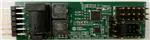
Peripheral Module Board Photo
Pmod is a trademark of Digilent Inc.
19-7768; Rev 0; 2/16
Benefits and Features
●● Up to 12 12-Bit ADC Programmable Inputs
●● Up to 12 12-Bit DACs with 25mA Current Capability
• 70mA max at +12V with On-Board Power Supply
• 30mA typ at -12V with On-Board Power Supply
• Use External Power Supply at VDDIO (VDDIO
Jumper Removed) if More Current is Needed
●●
●●
●●
●●
●●
●●
●●
●●
●●
●●
Up to 12 Digital I/Os
Up to 12 Comparator Inputs
Internal or External Reference for ADC and DAC
Individually Selectable ADC References for Each Port
Internal Temperature Sensor
(-40°C to +125°C, ±3°C Accuracy)
Two Remote Temperature-Measurement Controllers
(-40°C to +150°C, ±3°C Accuracy)
2x6-Pin Pmod-Compatible Connector (SPI)
RoHS Compliant
Proven PCB Layout
Fully Assembled and Tested
Ordering Information appears at end of data sheet.
�Evaluates: MAX11311
MAX11311PMB# Peripheral Module
Detailed Description
X1
SPI Interface
The MAX11311PMB# Pmod can plug directly into a
Pmod-compatible port (configured for SPI) through the
X1 connector. For information on the SPI protocol, refer
to the MAX11311 IC data sheet.
●● Connector X1 provides connection of the module to
the Pmod host. See Table 1 and Figure 1 for detailed
description.
●● Connector JP1 provides selection of +3.3V either
from the PMOD_SUPPLY or an external supply, X2.
●● Connectors SV1 and SV2 provide connection to the
IC pins (MAX11311 ports 0–11). Connector SV3 is
ground.
●● Connectors EXT_TEMP1 and EXT_TEMP2 provide
connection to the external temperature sensors.
●● Connector VDDIO provides connection to the
AVDDIO pins of the device, which is connected to
the +12V power supply
●● Connector VSSIO provides connection to the AVSSIO
pins of the device, which is the analog negative supply
for mixed-signal ports. Install VSSIO from 1 to 2 to
connect AVSSIO to ground. Install VSSIO from 2 to 3
to connect AVSSIO to -12V.
INTB
7
1
CS
8
2
MOSI
9
3
MISO
CNVTB
10
4
SCLK
GND
11
5
GND
3.3V
.
12
6
3.3V
SPI
Figure 1. X1: Pmod SPI Connector Pin Configuration
Table 1. Connector X1 (SPI Communication)
PIN
SIGNAL
1
CS
DESCRIPTION
Chip Select. Assert low to enable the SPI interface.
2
MOSI
MAX11311 Serial Data Input
3
MISO
MAX11311 Serial-Data Output
4
SCLK
MAX11311 Serial-Clock Input
5, 11
GND
Ground
6, 12
+3.3V
+3.3V Power Supplies
7
INTB
Interrupt Open-Drain Output. Asserted low when the MAX11300 issues an interrupt.
8
—
No Connection
9
—
No Connection
10
CNVTB
www.maximintegrated.com
ADC Conversion Control Input. Assert low to initiate an ADC conversion.
Maxim Integrated │ 2
�Evaluates: MAX11311
MAX11311PMB# Peripheral Module
Default Jumper Setting
Visit www.maximintegrated.com/evkitsoftware to
download the latest version of the Munich GUI software.
Refer to the MAX11311PMB# peripheral module and
Munich (USB2PMB1) adapter board Quick Start Guide for
step-by-step evaluation using the Munich GUI.
Verify that all jumpers are in their default positions, as
follows:
1) Jumper VDDIO: Connect from VDDIO to +12V
2) Jumper VSSIO: Connect from VSSIO to GND
3) Jumpers EXT_TEMP1 and EXT_TEMP2: Open
4) Jumper JP1: Connect PMOD_SUPPLY to +3.3V,
JP1-1 to JP1-2.
External Power Supply
The on-board power supply provides 70mA max current
at VDDIO = +12V. If additional current is needed, use an
external power supply by removing the jumper connecting
VDDIO to +12V and connecting a +12V external power
supply to the VDDIO pin.
Power Supplies
The Pmod contains the MAX8752 step-up DC-DC converter
(U3), which upconverts the +3.3V power supply from the
Pmod X1 connector to +13V. The MAX5084 (U2) linear
regulator then regulates the +13V input to +5V output voltage,
providing power supply to the positive analog supply AVDD
of the IC. Another MAX5084 (U1) provides a +12V power
supply to the positive analog supply of the mixed-signal
ports (AVDDIO) of the IC. Additionally, the MAX629 (U5)
provides -12V power supply to the VSSIO from +3.3V
input. For bipolar applications, use an external power
supply to provide negative voltage for AVSSIO. See Figure 2.
For bipolar applications, remove the jumper from the
VSSIO pin to GND and connect it from pin 2 to pin 3.
See Figure 2 and refer to the MAX11311 IC data sheet
for details.
External Temperature Sensors
Two-pin connector vertical headers, EXT_TEMP1 and
EXT_TEMP2, are provided to measure the environment
temperature. Connect the base and collector of diodeconnected transistors, such as the 2N3906 to the TEMP1
or TEMP2 pin and the emitter to the EXT pin to measure
the external temperature. See Figures 3 and 4.
Software Graphical User Interface (GUI)
The Munich software GUI is provided to facilitate evaluation
of the Pmod.
+3.3V (FROM
USB2PMB2
BOARD X1
CONNECTOR)
JP1
MAX8752(U3)
+13V
+5V(AVDD)
MAX5084(U2)
+3.3V (FROM
EXTERNAL
POWERY
SUPPLY)
+3.3V(DVDD)
MAX5084(U1)
MAX629 (U5)
+12V(VDDIO)
-12V (VSSIO)
MAX11311PMB
VSSIO (GND OR -12V)
Figure 2. Power-Supply Block Diagram
www.maximintegrated.com
Maxim Integrated │ 3
�MAX11311PMB# Peripheral Module
Evaluates: MAX11311
BASE AND COLLECTOR ARE CONNECTED
TOGETHER (RED WIRE)
EMITTER
(BLACK WIRE)
Figure 3. 2N3906 Diode-Connected Transistor Assembly (Not Included)
Figure 4. External Temperature Sensor Using Diode-Connected Transistor (Not Included)
www.maximintegrated.com
Maxim Integrated │ 4
�Evaluates: MAX11311
MAX11311PMB# Peripheral Module
Component Suppliers
SUPPLIER
WEBSITE
Pulse Electronics
www.pulseelectronics.com
TDK Corp.
www.component.tdk.com
TE Connectivity
www.te.com
Note: Indicate that you are using the MAX11311PMB# when contacting these component suppliers.
Component List, PCB Files, and
Schematics
See the following links for component information, PCB
files, and schematic:
●● MAX1311PMB EV BOM
●● MAX1311PMB EV PCB Layout
●● MAX1311PMB EV Schematic
www.maximintegrated.com
Ordering Information
PART
MAX11311PMB#
TYPE
Peripheral Module
USB2PMB1#
Munich Adapter Board
MAX11311SYS1#
Peripheral Module and
Munich Adapter Board
#Denotes RoHS compliant.
Maxim Integrated │ 5
�Evaluates: MAX11311
MAX11311PMB# Peripheral Module
Revision History
REVISION
NUMBER
REVISION
DATE
0
2/16
DESCRIPTION
Initial release
PAGES
CHANGED
—
For pricing, delivery, and ordering information, please contact Maxim Direct at 1-888-629-4642, or visit Maxim Integrated’s website at www.maximintegrated.com.
Maxim Integrated cannot assume responsibility for use of any circuitry other than circuitry entirely embodied in a Maxim Integrated product. No circuit patent licenses
are implied. Maxim Integrated reserves the right to change the circuitry and specifications without notice at any time.
Maxim Integrated and the Maxim Integrated logo are trademarks of Maxim Integrated Products, Inc.
© 2016 Maxim Integrated Products, Inc. │ 6
�TITLE: Bill of Materials
DATE: 10/05/2015
DESIGN: max11311pmb_evkit_b
ITEM REF_DES
1 C1, C2, C5, C15, C24
2 C3, C7, C8, C11, C14, C20
DNI/
DNP QTY MFG PART #
-
5 C1608X5R1A106K TDK
-
GRM188R71E105
KA12D;
CGA3E1X7R1E105 MURAT
6K
A
1UF
C4, C6, C9, C10, C12, C16,
C17, C19, C21-C23, C25,
C27, C28, CP2, CP8, CP9,
3 CP13
-
4 C13, C18
-
5 CP1, CP5, CP10-CP12
MANUF
ACTURE
R
VALUE
-
C0603C104K4RAC
;
GCM188R71C104
KA37;
C1608X7R1C104K
;
GRM188R71C104
K; C0603X7R16018 104KNE
10UF
KEMET/
MURAT
A/TDK/
VENKEL
LTD.
0.1UF
GRM21BR61E475 MURAT
2 KA
A
4.7UF
PANASO
NIC/YAG
ECJ-2FF1A106Z; EO
CC0805ZKY5V6BB PHYCO
51
MP
10UF
DESCRIPTION
CAPACITOR; SMT (0603);
CERAMIC CHIP; 10UF; 10V;
TOL=10%; MODEL=; TG=-55
DEGC TO +85 DEGC; TC=X5R
CAPACITOR; SMT (0603);
CERAMIC CHIP; 1UF; 25V;
TOL=10%; MODEL=GRM SERIES;
TG=-55 DEGC TO +125 DEGC;
TC=X7R
CAPACITOR; SMT (0603);
CERAMIC CHIP; 0.1UF; 16V;
TOL=10%; TG=-55 DEGC TO +125
DEGC; TC=X7R;
CAPACITOR; SMT (0805);
CERAMIC CHIP; 4.7UF; 25V;
TOL=10%; MODEL=X5R; TG=-55
DEGC TO +125 DEGC; TC=+/
CAPACITOR; SMT (0805);
CERAMIC CHIP; 10UF; 10V;
TOL=+80%-20%; MODEL=Y5V;
TG= -30 DEGC TO +85 DEGC; T;
�6 CP3
-
7 CP4
-
8 CP6
-
9 CP7
-
10 CP14
-
11 CP15
-
12 D1
-
13 D2, D3
-
C1608X5R1E225K
;
TMK107ABJ225K
1 A-T
C0603C224K3RAC
;
GMC10X7R224K2
5;
GRM188R71E224
KA88;
C1608X7R1E224K
1 08
TDK/TAI
YO
YUDEN 2.2UF
CAPACITOR; SMT (0603);
CERAMIC CHIP; 2.2UF; 25V;
TOL=10%; MODEL=; TG=-55
DEGC TO +85 DEGC; TC=X5R
CAPACITOR; SMT (0603);
CERAMIC CHIP; 0.22UF; 25V;
TOL=10%; TG=-55 DEGC TO +125
DEGC; TC=X7R
CAPACITOR; SMT; 0603;
CERAMIC; 20pF; 100V; 5%; C0G; C0603HQN101- VENKEL
55degC to + 125degC; 0 +/1 200JNP
LTD.
20PF
30PPM/degC
CAPACITOR; SMT; 0603;
CERAMIC; 1200pF; 50V; 10%;
C0G; -55degC to + 125degC; 0 +/C0603C0G500VENKEL
1 122KNP
LTD.
1200PF 30PPM/degC
CAPACITOR; SMT (0805);
CERAMIC CHIP; 2.2UF; 50V;
TOL=10%; MODEL=; TG=-55
1 C2012X7R1H225K TDK
2.2UF
DEGC TO +125 DEGC; TC=X7R
CAPACITOR; SMT (0603);
CERAMIC CHIP; 150PF; 100V;
TOL=10%; MODEL=C0G; TG=-55
1 C0603C151K1GAC KEMET 150PF
DEGC TO +125 DEGC; TC=+
TOSHIB CRS10I30 DIODE; SCH; SMT (SOD-123F);
A
PIV=30V; IF=1A
1 CRS10I30A
A
ON
SEMICO
DIODE; SCH; SURFACE MOUNT
NDUCT MBRS540 SCHOTTKY POWER RECTIFIER;
2 MBRS540T3G
OR
T3
SMC; PIV=40V; IF=5A
KEMET;
MURAT
A; TDK 0.22UF
�14 EXT_TEMP1, EXT_TEMP2
-
2 PEC02SAAN
SULLINS
15 ICD
-
1 M22-2510605
-
DF11-6DP1 2DSA(24)
HARWIN
HIROSE
ELECTRI
C CO
LTD
16 J1
CONNECTOR; MALE; THROUGH
PEC02SA HOLE; BREAKAWAY; STRAIGHT;
AN
2PINS
CONNECTOR; MALE; THROUGH
HOLE; 2MM PITCH; SIL VERTICAL
PIN HEADER ASSEMBLY;
M222510605 STRAIGHT; 6PINS
CONNECTOR; MALE; THROUGH
HOLE; DF11 SERIES; DOUBLEDF11-6DP- ROW CONNECTOR; STRAIGHT;
2DSA(24) 6PINS
17 JP1, VSSIO
-
2 PEC03SAAN
CONNECTOR; MALE; THROUGH
PEC03SA HOLE; BREAKAWAY; STRAIGHT;
SULLINS AN
3PINS
18 L1
-
1 DR74-3R3-R
COILTR
ONICS 3.3UH
19 L2
-
20 R1, R4
-
21 R2, R5, R8
-
INDUCTOR; SMT; FERRITE CORE;
3.3UH; TOL=+/-20%; 3.94A
COILTR
INDUCTOR; SMT; FERRITE CORE;
1 DR74-470-R
ONICS 47UH
47UH; TOL=+/-20%; 1.15A
SUSUM
U CO
RG1005P-101-B- LTD./PA
NASONI
T5; ERARESISTOR, 0402, 100 OHM, 0.1%,
2 2AEB101X
C
100 25PPM, 0.0625W, THICK FILM
VISHAY
DALE;
CRCW0402100KF YAGEO
PHICOM
K; RC0402FRRESISTOR; 0402; 100K; 1%;
3 07100KL
P
100K
100PPM; 0.0625W; THICK FILM
�22 R3
-
23 R6, R9, R11-R15
-
CRCW040212K0F VISHAY
1K
DALE
12K
VISHAY
DALE;
CRCW040210K0F YAGEO
PHICOM
K; RC0402FR7 0710K
P
10K
24 R7
-
25 R10
-
26 RG
-
CRCW040240K2F
1K
CRCW08052R00F
1N
CRCW04020000Z
1S
-
YAGEO
RC0402JR-070RL; PHYCO
MP/VEN
CR0402-16W6 000RJT
KEL LTD.
27 RI1-RI6
VISHAY
DALE
40.2K
VISHAY
DALE
VISHAY
DALE
RESISTOR, 0402, 12K OHM, 1%,
100PPM, 0.0625W, THICK FILM
RESISTOR; 0402; 10K; 1%;
100PPM; 0.0625W; THICK FILM
RESISTOR; 0402; 40.2K OHM; 1%;
100PPM; 0.063W; THICK FILM
RESISTOR, 0805, 2 OHM, 1%,
2 100PPM, 0.125W, THICK FILM
RESISTOR; 0402; 0 OHM; 0%;
0 JUMPER; 0.063W; THICK FILM
RESISTOR; 0402; 0 OHM; 5%;
0 JUMPER; 0.063W; THICK FILM
28 SV1-SV3
-
3 22-28-4063
29 U1,U2
-
2 MAX5084ATT+T
CONNECTOR; MALE; THROUGH
HOLE; FLAT VERTICAL
22-28MOLEX 4063
BREAKAWAY; STRAIGHT; 6PINS
IC; VREG; LOW-QUIESCENTMAX5084 CURRENT LINEAR REGULATOR;
MAXIM ATT+T
TDFN6
1 MAX8752ETA+
MAX8752 IC; CONV; TFT LCD STEP-UP DCMAXIM ETA+
DC CONVERTER; TDFN8-EP
30 U3
-
�EVKIT PART-IC; MAX11311;
PACKAGE OUTLINE: 21-0140;
PACKAGE CODE: T3255-4;
MAX1131 TQFN32-EP; NO FINAL
1
DATASHEET
IC; CONV; LOW-POWER HIGHVOLTAGE BOOST OR INVERTING
MAX629E DC-DC CONVERTER; NSOIC8
SA+
150MIL
IC; CTRL; ATMEL 8-BIT AVR
MICROCONTROLLER WITH 2K
BYTES IN-SYSTEM
ATTINY25- PROGRAMMABLE FLASH;
20SU
WSOIC8
CONNECTOR; MALE; THROUGH
923345- HOLE; JUMPER WIRE; STRAIGHT;
01-C
2PINS
CONNECTOR; THROUGH HOLE;
POST TERMINAL STRIP
TSW-106- ASSEMBLY; RIGHT ANGLE;
08-S-D-RA 12PINS;
CONNECTOR; FEMALE;
KLDXTHROUGH HOLE; DC POWER
0202-B
JACK; RIGHT ANGLE; 3PINS
RESISTOR; 0402; 0 OHM; 0%;
0 JUMPER; 0.063W; THICK FILM
31 U4
-
1 MAX11311
MAXIM
32 U5
-
1 MAX629ESA+
MAXIM
33 U7
-
1 ATTINY25-20SU
ATMEL
34 VDDIO
-
1 923345-01-C
?
35 X1
-
TSW-106-08-S-D1 RA
SAMTEC
36 X2
-
37 RU1, RU2
DNP
1 KLDX-0202-B
KYCON
CRCW04020000Z VISHAY
DALE
2S
38 U6
DNP
MICROC PIC10F20 IC; CTRL; 6-PIN; 8-BIT FLASH
1 PIC10F200-I/OTG HIP
0-I/OTG MICROCONTROLLER; SOT23-6
�������VDDIO
0.1UF
0.1UF
4.7UF
GND
GND
AGND
AGND
C12
C17
AGND
C27
10UF
0.1UF
AGND
AGND
C6
C5
0.1UF
C10
10UF
C11
0.1UF
AGND
6
5
4
1UF
OUT
OUT_SENSE
SET
IN
PB5
PB2
PB3
PB1
PB4
PB0
SV3
1
2
3
EN
GND
22-28-4063
C9
C8
7
6
5
0.1UF
1UF
AGND AGND
27
12
VDDIO
AVDD
IN
D0N
11
D0P
10
D1P
15
D1N
16
PIXI0
14
RI3
0
RI4
0
7
CNVTB
5
AD1_DOUT
PIXI1
17
PIXI2
19
4
AD0_CSB
3
SCL_SCLK
PIXI3
20
PIXI4
2
SDA_DIN
21
PIXI5
22
6
INTB
PIXI6
24
PIXI7
25
PIXI8
28
PIXI9
29
PIXI10
30
PIXI11
31
AGND
EP
VSSIO
PEC03SAAN
3
2
1
-12V
C14
1UF
AGND
IN
SPI_MOSI
GND
1
2
SV1
1
2
3
4
5
6
22-28-4063
+3V3
SV2
1
2
3
4
5
6
IN
GND
IN
PEC02SAAN
GND
22-28-4063
R12
C15
C16
C21
C22
R13
10K
VSS_IO
SPI_MISO
SPI_SCLK
IN
0.1UF
0.1UF
0.1UF
0.1UF
AGND
AGND
AGND
AGND
AGND
0.1UF
SPI_CS_ADC
IN
1
3
6
IN
VDD
R14
GP1/ICSPCLK
GP2/T0CKI/FOSC4
AGND
4
IN
GP3/MCLR/VPP
+3V3
10K
DNI
U6
PIC10F200-I/OTG
GP0/ICSPDAT
VSS
C23
10UF
C28
10K
GND
33
0
VSS_IO
IN
23
RI6
AGND1
0
26
IN
AGND
RI5
IN
EXT_TEMP2
PEC02SAAN
0
IN
1
2
DF11-6DP-2DSA(24)
1 1
2 2
3 3
4 4
5 5
6 6
IN
5
18
VDDIO
RI2
SPI_MISO
SPI_SCLK
RESET
EXT_TEMP1
MAX11311
IN
SPI_SCLK
SPI_MISO
SPI_MOSI
+3V3
2
8
ADC_INT_REF
0
9
IN
DREF_PAD_F
RI1
IN
AGND
J1
U4
IN
GND
6
5
4
3
2
1
AGND
RU1
0
DNI
GND
GND
EP
AGND
1
2
3
+13V
IN
U7
ATTINY25-20SU
VCC
SPI_CS_ADC
AGND
32
INTB
1UF
13
SPI_MOSI
C7
10K
IN
C1
1UF
+3V3
SPI_CS_ADC IN
SPI_SCLK
C3
U2
DGND
SPI_MISO
C4
0.1UF
MAX5084ATT+T
1
CNVTB
AGND
EN
GND
AGND
DVDD
RU2
0
DNI
AGND
SET
RESET
12K
C18
4.7UF
OUT_SENSE
R3
C13
0.1UF
1
2
3
IN
EP
GND
C19
OUT
4
AGND
C20
1UF
+3V3
+12V
0
6
5
4
7
R1
100
1
AGND
RG
R2
100K
+3V3
R11
8
+3V3
MAX5084ATT+T
7
10UF
+13V
U1
2
C2
SPI_MOSI
R15
10K
GND
GND
C25
0.1UF
GND
+3V3
SPI_CS_ADC
SPI_MISO
SPI_SCLK
6
IN
CP2
0.1UF
R7 GND
40.2K
CP7
+5V
1
7
COMP
LDO
CP6
1200PF
20PF
GND
GND
FB
2
GND
EP
4
9
SUP
8
+3V3
CP8
0.1UF
GND
CP4
CP3
0.22UF
2.2UF
GND
GND
R5
100K
CP5
10UF
GND
R6
10UF
CP11
GND
GND
GND
2
10UF
1
SHDN
1
U5
MAX629ESA+
LX
7
5
2
CP14
2.2UF
R10
2
D2
ISET
FB
POL
4
MBRS540T3
R8
100K
REF
GND
-12V
D3
MBRS540T3
GND
3
PMOD CONNECTOR
A
0.1UF
CP12
10K
GND
IN
L2
47UH
C
100
MAX8752ETA+
CP13
+3V3
A
GND
U3
A
+3V3
C
GND
R4
5
10UF
CRS10I30A
C
2
+3V3
8
CP1
10UF
3.3UH
+3V3
6 GND
1
+13V
D1
LX
GND
CP10
L1
SHDN
CP9
0.1UF
+3V3
+3V3
+3V3
3
+3V3
GND
IN
NEGATIVE VOLTAGE FOR VSSIO
VCC
STEP-UP FOR VDDIO AND AVDD
IN
ICD
M22-2510605
1
2
3
4
5
6
CP15
150PF
C24
10UF
GND
EXTERNAL SUPPLY
3V TO 5V HAS TO
MATCH SPI-LEVELS
X2
KLDX-0202-B
1
1
3
3
2
2
R9
10K
GND
PMOD_SUPPLY
X1
TSW-106-08-S-D-RA
+3V3
JP1
IN
PEC03SAAN
1
2
3
PMOD_SUPPLY
SPI_SCLK
SPI_MISO
SPI_MOSI
SPI_CS_ADC
IN
IN
GND
11
11
12
12
9
9
10
10
7
7
8
8
IN
5
5
6
6
IN
3
3
4
4
IN
1
1
2
2
GND
IN
PMOD_SUPPLY
IN
CNVTB
IN
INTB
�


 工商网监
湘ICP备2023018690号
工商网监
湘ICP备2023018690号
