EVALUATION KIT AVAILABLE
Click here to ask about the production status of specific part numbers.
MAX14906
Quad-Channel Industrial
Digital Output/Digital Input
General Description
Benefits and Features
The MAX14906 is an IEC 61131-2 compliant, high-speed,
four-channel industrial digital output, digital input device
that can be configured on a per-channel basis as a highside (HS) switch, push-pull (PP) driver, or a Type 1 and 3,
or Type 2 digital input. The MAX14906 is specified for operation with a supply voltage up to 40V and is tolerant to
65V.
● Per-Channel Configurability Enables Wide Range of
Applications
• Digital Output: High-Side (HS) Switch or Push-Pull
(PP) Driver
• Digital Input: Software Selectable Type 1 and 3, or
Type 2
• Current Limit Settable from 130mA to 1.2A
• Serial (SPI) or Direct Operation Using Pins
• Independent Channel Powering
The high-side switch current limiting is settable from
130mA to 1.2A with the option of 2x load inrush current.
The high-side driver on-resistance is 120mΩ (typ) at 25°C
ambient temperature. Optional push-pull operation allows
high speed driving of cables and fast discharge of load
capacitance. For digital input operation, current sinks for
2.3mA (Type 1 and 3) or 7mA (Type 2) are provided.
The SPI interface has a built-in chip addressing decoder,
allowing communication with multiple MAX14906 devices
utilizing a shared SPI with a common chip select (CS). The
SPI interface provides flexibility for global and per-channel configuration and diagnostics, including supply overvoltage and undervoltage detection, wire-break or openwire detection, thermal overload and current limit reporting, and more. For high-speed operation, the digital input
and output states can be monitored and changed directly
using pins for increased system speed and throughput.
Open-wire detection monitors open-wire/open-load conditions with switches in the off state. LED drivers provide indication of per-channel fault, status, and supply undervoltage conditions. Internal active clamps allow for fast turnoff of inductive loads. Integrated line-to-ground and lineto-line surge protection only requires a TVS on VDD.
The MAX14906 is available in a compact 48-pin 7mm x
7mm QFN package.
Applications
●
●
●
●
●
Industrial Digital Output and Input Module
Configurable Digital Input/Output
Motor Control
PLC Systems
Distributed Control Systems (DCS)
● Fault Tolerant with Built-In Diagnostics
• Per-Channel Diagnostics
• Integrated Voltage Supply Monitoring and Short-toVDD Detection
• Open-Wire/Open-Load Detection
• Thermal Shutdown Protection
• Watchdog Timer
• 5-Bit CRC Code Generation and Checking for SPI
Error Detection
● High Integration Reduces BOM Count and PCB
Space
• Integrated LDO Compatible with 5V Logic Devices
• Internal Active Clamps for Fast Inductive Load
Turn-Off
• 0.6μs (typ) DO and 1μs (typ) DI Propagation Delays
• Addressable SPI
• 7mm x 7mm TQFN Package
● Reduced Power and Heat Dissipation
• Low RDSON for High-Side Switches, 120mΩ (typ)
• Accurate Output Current Limiting
• Accurate Input Current Sinks, Type 1 and 3, or
Type 2
● Robust Design
• 10V to 40V Operating Supply Range, 65V Tolerant
• SafeDemagTM Allows Fast Turn-Off of Unlimited
Inductance
• ±16kV Air-Gap ESD and ±8kV Contact ESD
• ±1kV Surge Tolerant Using TVS Protection on VDD
to GND
• -40°C to +125°C Operating Temperature
Ordering Information appears at end of datasheet.
SafeDemag is a trademark of Maxim Integrated Products, Inc.
19-100736; Rev 2; 8/21
�MAX14906
Quad-Channel Industrial
Digital Output/Digital Input
Quad Industrial Digital Output, Digital Input
24V
24V
3.3V
1µF
0.1µF
0.1µF
24V
24V
1µF
1µF
1µF
10µF
36V
24.9kΩ
VL EN REGEN
VDD
V5
VDDOK VLED
VDD4 VDD3
VDD2 VDD1
VDD
CRCEN
GPIO
READY
10kΩ
G4
GPIO
D4
DOI4
GPIO
D3
DOI4
GPIO
D2
GPIO
D1
GPIO
SYNCH
G3
A0
CONTROLLER
DOI4
MAX14906
A1
DOI3
DOI3
DOI3
CS
CS
SCLK
CLK
MOSI
SDI
MISO
3.3V
SDO
G2
DOI2
10kΩ
FAULT
INT
DOI2
DOI2
5.6kΩ
L4
G1
5.6kΩ
L3
DOI1
5.6kΩ
DOI1
DOI1
L2
5.6kΩ
L1
www.maximintegrated.com
SLED
FLED
GND
PGND
EP
Maxim Integrated | 2
�MAX14906
Quad-Channel Industrial
Digital Output/Digital Input
Absolute Maximum Ratings
VDD, VDD1, VDD2, VDD3, VDD4, VLED ................... -0.3V to +65V
DOI1, DOI2, DOI3, DOI4
VDD < VDD_OVTH .........................(VDD - 49V) to (VDD + 0.3V)
VDD > VDD_OVTH ...................................... -1V to (VDD + 0.3V)
V5, VL ....................................................................... -0.3V to +6V
SDI, CLK, CS, EN, A0, A1, SYNCH, REGEN .......... -0.3V to +6V
FAULT ...................................................................... -0.3V to +6V
D1, D2, D3, D4, SDO, READY ..................... -0.3V to (VL + 0.3V)
SLED, FLED, L1, L2, L3, L4, VDDOK ...... -0.3V to (VLED + 0.3V)
G1, G2, G3, G4 ............................ -0.3V to min(40V, VDD + 0.3V)
Continuous Current
DOI_ Load Current ........................................Internally Limited
All Pins other than DOI_ ............................. -100mA to +100mA
Inductive Demagnetization Energy (IDOI_ < 0.6A) ......... Unlimited
Continuous Power Dissipation (TA = +70ºC)
TQFN 48 (derate 40mW/°C above 70°C) ....................3200mW
Junction Temperature ........................................Internally Limited
Storage Temperature Range ..............................-65°C to +150°C
Lead Temperature (soldering, 10s)................................... +300°C
Soldering Temperature (reflow) ........................................ +260°C
Note 1: All voltages relative to GND.
Stresses beyond those listed under “Absolute Maximum Ratings” may cause permanent damage to the device. These are stress ratings only, and functional operation of the
device at these or any other conditions beyond those indicated in the operational sections of the specifications is not implied. Exposure to absolute maximum rating conditions for
extended periods may affect device reliability.
Package Information
48 TQFN
Package Code
T4877+6C
Outline Number
21-0144
Land Pattern Number
90-0130
Thermal Resistance, Four-Layer Board:
Junction to Ambient (θJA)
25°C/W
Junction to Case (θJC)
1°C/W
For the latest package outline information and land patterns (footprints), go to www.maximintegrated.com/packages. Note that a “+”, “#”, or “-” in the package code indicates
RoHS status only. Package drawings may show a different suffix character, but the drawing pertains to the package regardless of RoHS status.
Package thermal resistances were obtained using the method described in JEDEC specification JESD51-7, using a four-layer board. For detailed information on package thermal
considerations, refer to www.maximintegrated.com/thermal-tutorial.
Electrical Characteristics
(VDD = VDD1 = VDD2 = VDD3 = VDD4 = +10V to +40V, VLED = +3.0V to +40V, V5 = +4.5V to +5.5V, VL = +2.5V to +5.5V, TA = -40°C
to +125°C, unless otherwise noted. Typical values are at TA = +25ºC, VDD = VDD_ = VLED = +24V, VL = 3.3V, REGEN = Open, and
V5 = 5V.) (Note 2)
PARAMETER
SYMBOL
CONDITIONS
MIN
TYP
MAX
UNITS
VDD AND VDD_ SUPPLY VOLTAGES
Supply Voltage VDD and
VDD_
Normal Operating Conditions
VDD
Overvoltage Lockout Tolerance
10
40
VDD_OV
65
TH
All channels in HS mode, VDD = 40V,
REGEN = GND, DOI_ not loaded, no
load on V5
VDD Supply Current
IDD_ON
2.5
4.5
All channels in PP mode, VDD = 40V,
REGEN = GND, 10kHz switching, no load
on DOI_, no load on V5
4
7
All channels in DI mode, REGEN = GND
2.5
4.5
0.5
1.4
mA
43.5
45
V
VDD Supply Current
Increase
IDD_ON_IN
All G_ turn on
Overvoltage Lockout
Threshold
VDD_OVTH
VDD rising
www.maximintegrated.com
V
mA
41.5
Maxim Integrated | 3
�MAX14906
Quad-Channel Industrial
Digital Output/Digital Input
Electrical Characteristics (continued)
(VDD = VDD1 = VDD2 = VDD3 = VDD4 = +10V to +40V, VLED = +3.0V to +40V, V5 = +4.5V to +5.5V, VL = +2.5V to +5.5V, TA = -40°C
to +125°C, unless otherwise noted. Typical values are at TA = +25ºC, VDD = VDD_ = VLED = +24V, VL = 3.3V, REGEN = Open, and
V5 = 5V.) (Note 2)
PARAMETER
Overvoltage Lockout
Hysteresis
Undervoltage Lockout
Threshold
Undervoltage Lockout
Hysteresis
Undervoltage VDD
Warning Threshold
Undervoltage VDD
Warning Hysteresis
Undervoltage VDD Good
Threshold
Undervoltage VDD Good
Hysteresis
SYMBOL
CONDITIONS
MIN
VDD_OVHYST
TYP
MAX
1
VDD_UVLO_R
VDD rising
VDD_UVLO_F
VDD falling
V
9.6
7.9
VDD_UVHYST
1
VDD_WARN_R
VDD rising
VDD_WARN_F
VDD falling
14
1
VDD_GOOD_R
VDD rising
VDD_GOOD_F
VDD falling
V
V
17
15
VDD_GOOD_H
V
V
12
VDD_WARN_H
UNITS
1
V
V
LOGIC INTERFACE SUPPLY (VL)
VL Supply Voltage
VL
VL Supply Current
IVL
VL POR Threshold
VL_POR
2.5
5.5
V
18
40
µA
1
1.27
1.55
V
4.75
5.0
5.25
V
1
1.8
mA
All channels in active clamp PP mode,
REGEN = GND, all DOI_ switches ON
and unloaded
1.1
2
mA
All logic inputs high or low, logic outputs
unloaded
VL voltage falling
5V SUPPLY (V5)
V5 Supply Voltage
V5
V5 Supply Current in HS
Mode
IV5_ON_HS
V5 Supply Current in
Active-Clamp PP Mode
IV5_ON_PP_AC
REGEN = GND
All channels in HS mode, REGEN =
GND, all DOI_ switches ON and
unloaded
V5 Supply Current in
Simple PP Mode
IV5_ON_PP
All channels in simple PP mode, REGEN
= GND, all DOI_ switches ON and
unloaded
1.1
2
mA
V5 Supply Current in DI
Mode
IV5_ON_DI
All channels in DI mode, REGEN = GND,
all DOI_ at 30V
1.1
2
mA
V5 Undervoltage
Lockout Threshold
V5_UVLO
V5 rising
4.4
V
V5 Undervoltage
Lockout Hysteresis
V5UVLO_HYS
3.8
0.3
V
5V LINEAR REGULATOR (V5, REGEN)
V5 Regulator Output
Voltage
V5
V5 Regulator Current
Limit
ICL_V5
REGEN = open
25
IPU_REGEN
REGEN = GND
5
REGEN Pullup Current
www.maximintegrated.com
REGEN = open, 0mA to 20mA external
load current
4.75
5.0
5.25
V
mA
30
µA
Maxim Integrated | 4
�MAX14906
Quad-Channel Industrial
Digital Output/Digital Input
Electrical Characteristics (continued)
(VDD = VDD1 = VDD2 = VDD3 = VDD4 = +10V to +40V, VLED = +3.0V to +40V, V5 = +4.5V to +5.5V, VL = +2.5V to +5.5V, TA = -40°C
to +125°C, unless otherwise noted. Typical values are at TA = +25ºC, VDD = VDD_ = VLED = +24V, VL = 3.3V, REGEN = Open, and
V5 = 5V.) (Note 2)
PARAMETER
REGEN Threshold
SYMBOL
VTH_REGEN
CONDITIONS
REGEN rising
MIN
TYP
MAX
UNITS
1
1.6
2.5
V
120
240
mΩ
1
3
Ω
DRIVER OUTPUTS (DOI_)
High-Side OnResistance
RON_HS
HS or PP modes, IDOI_ = 500mA
Low-Side OnResistance
RON_LS
DoMode_ = 11 (Simple PP mode), IDOI_
= 100mA
Low-Side Output Low
Voltage
VOL_LS
DOI_ Clamp Voltage
VCL
ILK40_DOI
DOI_ Leakage
ILKDOI_ANA
Active clamp PP mode, IDOI_ = 100mA
1.2
Simple PP mode, IDOI_ = 100mA
0.4
V
Relative to VDD_, IDOI_ = 10mA, VDD_ <
VDD_OVTH
-63
-55
-49
Relative to GND, IDOI_ = 10mA,
VDD_OVTH < VDD_ < 60V
-6
-4.5
-3
VDD_ = 40V, HS mode, DOI_ = off, 0V <
DOI_ < VDD_
-60
+60
µA
VDD_ = 40V, low-leakage highimpedance mode, 0V < DOI_ < VDD_
-2.4
+2.4
μA
V
OFF STATE DIAGNOSTICS (DOI_)
IDIAG1
OWOffEn_ = 1, VDOI_ < 5V or VDOI_ >
9V, OWOffCs = 00, Both Open-Wire and
Short-to-VDD
20
60
120
IDIAG2
OWOffEn_ = 1, VDOI_ < 5V or VDOI_ >
9V, OWOffCs = 01, Both Open-Wire and
Short-to-VDD
60
100
180
IDIAG3
OWOffEn_ = 1, VDOI_ < 5V or VDOI_ >
9V, OWOffCs = 10, Both Open-Wire and
Short-to-VDD
200
300
440
IDIAG4
OWOffEn_ = 1, VDOI_ < 5V or VDOI_ >
9V, OWOffCs = 11, Both Open-Wire and
Short-to-VDD
460
600
760
OWOffEn_ = 1, IDOI_ = 0mA
5.8
6.7
7.6
V
5.8
V
Diagnostic Test Current
µA
DOI_ Open Voltage,
OWOff_
VOUT_OFF
Open-Wire Detection
Threshold, OWOff_
VTH_OWOFF
OWOffEn_ = 1
VTH_SHVDD1
ShVddEn_ = 1, ShtVddThr = 00
8.2
9
10
VTH_SHVDD2
ShVddEn_ = 1, ShtVddThr = 01
9.1
10
10.9
VTH_SHVDD3
ShVddEn_ = 1, ShtVddThr = 10
11
12
13
VTH_SHVDD4
ShVddEn_ = 1, ShtVddThr = 11
13
14
15
Short-to-VDD Detection
Threshold
www.maximintegrated.com
5
V
Maxim Integrated | 5
�MAX14906
Quad-Channel Industrial
Digital Output/Digital Input
Electrical Characteristics (continued)
(VDD = VDD1 = VDD2 = VDD3 = VDD4 = +10V to +40V, VLED = +3.0V to +40V, V5 = +4.5V to +5.5V, VL = +2.5V to +5.5V, TA = -40°C
to +125°C, unless otherwise noted. Typical values are at TA = +25ºC, VDD = VDD_ = VLED = +24V, VL = 3.3V, REGEN = Open, and
V5 = 5V.) (Note 2)
PARAMETER
SYMBOL
CONDITIONS
MIN
TYP
MAX
UNITS
DO HS or PP modes, CL_ = 01, OVL_ =
X, t > tINRUSH, see Table 2
130
175
220
DO HS or PP modes, CL_ = 01, OVL_ =
1, t < tINRUSH, see Table 2
300
350
400
DO HS or PP modes, CL_ = 10, OVL_ =
X, t > tINRUSH, see Table 2
300
350
400
DO HS or PP modes, CL_ = 10, OVL_ =
1, t < tINRUSH, see Table 2
600
700
800
DO HS or PP modes, CL_ = 00, OVL_ =
X, t > tINRUSH, see Table 2
600
700
800
DO HS or PP modes, CL_ = 00, OVL_ =
1, t < tINRUSH, see Table 2
1.2
1.4
1.6
DO HS or PP modes, CL_ = 11 OVL_ =
X, t > tINRUSH, see Table 2
1.2
1.4
1.6
DO HS or PP modes, CL_ = 11 OVL_ =
1, t < tINRUSH, see Table 2
2.4
2.8
3.2
DO PP modes
150
200
280
mA
DI mode, DOI_ rising
6.7
8.0
V
CURRENT LIMITING (DOI_)
HS Current Limit
LS Current Limit
ICLIM
ICLIM_LS
mA
A
DIGITAL INPUT (DOI_)
Threshold Voltage
VTH_DOI_DI
Hysteresis Voltage
VHYS_DOI_DI
Current Sink
DI mode
IDOI_DI_L
DI mode, Typ2Di = 0, 0V < VDOI_ < 5V
IDOI_DI_H
DI mode, Typ2Di = 0, 8V < VDOI_ < 40V,
VDOI_< VDD_
IDOI_DI_L
DI mode, Typ2Di = 1, 0V < VDOI_ < 5V
IDOI_DI_H
DI mode, Typ2Di = 1, 8V < VDOI_ < 40V,
VDOI_ < VDD_
1.2
0
2.0
2.3
0
6.0
V
2.6
2.6
7.5
7.0
mA
7.7
LOGIC INTERFACE I/O
Input Voltage High
VIH
Input Voltage Low
VIL
Input Threshold
Hysteresis
VIHYS
Input Pull-Down
Resistor
RIN_PD
0.7 x VL
0.3 x VL
0.11 x
VL
EN pin
Input Leakage
ILEAK
GND < VIN < VL
Output Logic High
VOH
ILOAD = -5mA
VOL
ILOAD = +5mA
Output Logic Low
V
110
200
-1
V
V
260
kΩ
+1
µA
VL - 0.33
V
0.33
V
Output Leakage D_
ILEAK_DOI
DO modes
-1
+1
μA
Output Leakage SDO
ILEAK_SDO
CS is high
-1
+1
μA
G_ driver clamp voltage to GND
43
59
V
GATE DRIVER (G_)
VDD Threshold for G_
Turn-on
www.maximintegrated.com
VDDTH_G
48
Maxim Integrated | 6
�MAX14906
Quad-Channel Industrial
Digital Output/Digital Input
Electrical Characteristics (continued)
(VDD = VDD1 = VDD2 = VDD3 = VDD4 = +10V to +40V, VLED = +3.0V to +40V, V5 = +4.5V to +5.5V, VL = +2.5V to +5.5V, TA = -40°C
to +125°C, unless otherwise noted. Typical values are at TA = +25ºC, VDD = VDD_ = VLED = +24V, VL = 3.3V, REGEN = Open, and
V5 = 5V.) (Note 2)
PARAMETER
SYMBOL
CONDITIONS
G_ On Voltage
VON_G
DO modes, DOI_ ≤ VDD_
G_ Off Switch
Resistance
RON_G
DI modes
MIN
TYP
VDD_ 14
MAX
UNITS
VDD_ 10
V
50
Ω
OPEN-DRAIN OUTPUTS (FAULT, VDDOK, READY)
Output Logic Low
(FAULT, VDDOK)
VODL
ILOAD = +5mA
Output Logic High
(READY)
VODH
ILOAD = -5mA
Leakage (FAULT)
IODL
Open-drain output off, VOD = 5.5V
-1
+1
µA
Leakage (VDDOK)
IODL
Open-drain output off, VOD = 40V
-5
+5
µA
Leakage (READY)
IODL
Open-drain output off, VOD = GND
-1
+1
µA
3.0
VDD
V
1
μA
0.33
VL - 0.33
V
V
LED DRIVERS (L_, FLED, SLED)
LED Supply Voltage
VLED
LED Supply Current
ILED
VLED = 40V, SLED = Off, FLED = Off
L_ Voltage High
VOH_L
L_ = On, IL_ = 5mA
L_ Off Leakage Current
ILEAK_L
L_ = Off, VL_ = 0V
SLED Output Voltage
Low
SLED Off Leakage
Current
FLED Output Voltage
Low
FLED Off Leakage
Current
VOL_SLED
ILEAK_SLED
VOL_FLED
ILEAK_FLED
VLED 0.33
V
SLED = On, ISLED = 5mA
SLED = Off, VSLED = VLED
FLED = On, IFLED = 5mA
FLED = Off, VFLED = VLED
5
µA
0.33
V
5
µA
0.33
V
5
μA
DO MODES PROPAGATION DELAY (D_ or SYNCH to DOI_)
DOI Output Propagation
Delay Low-to-High
tPD_LH
Delay from D_ (or SYNCH) to DOI_ rising
by 0.5V, HS or PP modes
0.4
1.5
µs
DOI Output Propagation
Delay High-to-Low
tPD_HL
Delay between D_ switching low (or
SYNCH high) to DOI_ falling by 0.5V,
VDD_ = 24V, RL = 10kΩ, CL = 0.1nF, HS
or PP modes
0.6
1.5
µs
HS or PP modes, 20% to 80% VDD_,
VDD_ = 24V, RL = 10kΩ, CL = 0.1nF
0.6
1.5
µs
DOI Output Rise Time
DOI Output Fall Time
tR
tF
HS modes, 80% to 20% VDD_, VDD_ =
24V, RL = 10kΩ, CL = 0.1nF
1
PP modes, 80% to 20% VDD_, VDD_ =
24V, RL = 10kΩ, CL = 0.1nF
0.9
2
0.9
1.8
µs
DI MODES PROPAGATION DELAY (DOI_ to D_)
Propagation Delay Highto-Low
www.maximintegrated.com
tPD_HL_DI
DI modes, SYNCH = high, delay from
DOI_ falling to 5V to D_ low
µs
Maxim Integrated | 7
�MAX14906
Quad-Channel Industrial
Digital Output/Digital Input
Electrical Characteristics (continued)
(VDD = VDD1 = VDD2 = VDD3 = VDD4 = +10V to +40V, VLED = +3.0V to +40V, V5 = +4.5V to +5.5V, VL = +2.5V to +5.5V, TA = -40°C
to +125°C, unless otherwise noted. Typical values are at TA = +25ºC, VDD = VDD_ = VLED = +24V, VL = 3.3V, REGEN = Open, and
V5 = 5V.) (Note 2)
PARAMETER
Propagation Delay Lowto-High
SYMBOL
tPD_LH_DI
CONDITIONS
MIN
DI modes, SYNCH = high, delay from
DOI_ rising to 8V to D_ high
TYP
MAX
UNITS
1.1
2
µs
SPI TIMING CHARACTERISTICS (Figure 1)
CLK Clock Period
tCLK
100
ns
CLK Pulse Width High
tCH
40
ns
CLK Pulse Width Low
tCL
40
ns
CS Fall to CLK Rise
Time
tCSS
40
ns
SDI Hold Time
tDH
10
ns
SDI Setup Time
tDS
10
ns
SDO Propagation Delay
tDO
CL = 10pF, CLK falling edge to SDO
stable
SDO Rise and Fall
Times
tFT
CL = 10pF
CS Hold Time
CS Pulse Width High
30
1
ns
ns
tCSH
40
ns
tCSPW
40
ns
WATCHDOG TIMING CHARACTERISTICS
WDTo = 01
Watchdog Timeout
Watchdog Timeout
Accuracy
tWD
tWD_ACC
200
WDTo = 10
600
WDTo = 11
1200
SynchWDEn = 1, see Config2 register for
watchdog timeout
-30
ms
+30
%
LED MATRIX TIMING CHARACTERISTICS
LED Driver Scan Rate
fLED
Update rate for each LED
1
kHz
170
°C
15
°C
150
°C
10
°C
165
ºC
THERMAL PROTECTION
Driver Thermal
Shutdown Temperature
Driver Thermal
Shutdown Hysteresis
TJSHDN
Junction temperature rising
TJSHDN_HYST
Chip Thermal Shutdown
TCSHDN
Chip Thermal Shutdown
Hysteresis
TCSHDN_HYS
LDO Thermal Shutdown
TLDSHDN
Temperature rising
T
EMC PROTECTION
ESD
www.maximintegrated.com
VESD
DOI_ pin, IEC 61000-4-2, Contact
Discharge, add a 470pF capacitor on
each DOI_ to GND (Note 3)
±8
DOI_ pin, IEC 61000-4-2 Air-Gap
Discharge (Note 3)
±16
All pins, Human Body Model
±2
kV
Maxim Integrated | 8
�MAX14906
Quad-Channel Industrial
Digital Output/Digital Input
Electrical Characteristics (continued)
(VDD = VDD1 = VDD2 = VDD3 = VDD4 = +10V to +40V, VLED = +3.0V to +40V, V5 = +4.5V to +5.5V, VL = +2.5V to +5.5V, TA = -40°C
to +125°C, unless otherwise noted. Typical values are at TA = +25ºC, VDD = VDD_ = VLED = +24V, VL = 3.3V, REGEN = Open, and
V5 = 5V.) (Note 2)
PARAMETER
SYMBOL
Surge
VSURGE
CONDITIONS
MIN
DOI_ to PGND or Earth GND, IEC
61000-4-5 (42Ω/0.5μF) (Note 4)
TYP
MAX
±1
UNITS
kV
Note 2: All units are production tested at TA = +25ºC. Specifications over temperature are guaranteed by design.
Note 3: Bypass VDD and VDD_ pins to GND with 1μF capacitor as close as possible to the device for high ESD protection. If an external
transistor is used on VDD_, place the FET as close to VDD_ as possible with 1μF capacitor on the other side of the FET to
PGND.
Note 4: At typical application value of VDD = 24V with a TVS protection on VDD to GND.
CS
tCSPW
tCLK
tCSS
tCL
tCSH
tCH
CLK
tDS
tDH
SDI
tDO
SDO
tFT
Figure 1. SPI Timing Diagram
www.maximintegrated.com
Maxim Integrated | 9
�MAX14906
Quad-Channel Industrial
Digital Output/Digital Input
Typical Operating Characteristics
(VDD = VDD_ = VLED = +24V, VL = +5V, REGEN = GND, V5 = +5V, no load on V5, TA = +25ºC, unless otherwise noted.)
www.maximintegrated.com
Maxim Integrated | 10
�MAX14906
Quad-Channel Industrial
Digital Output/Digital Input
Typical Operating Characteristics (continued)
(VDD = VDD_ = VLED = +24V, VL = +5V, REGEN = GND, V5 = +5V, no load on V5, TA = +25ºC, unless otherwise noted.)
www.maximintegrated.com
Maxim Integrated | 11
�MAX14906
Quad-Channel Industrial
Digital Output/Digital Input
Pin Configuration
MAX14906
SYNCH
SDI
CS
CLK
SDO
V5
GND
FAULT
REGEN
EN
READY
VL
TOP VIEW
36
35 34
33
32
31
30 29
28
27
26
25
D3
37
24 D2
PGND
38
23 PGND
DOI3
39
22 DOI2
DOI3
40
21 DOI2
VDD3
41
20 VDD2
G3
42
G4
43
18 G1
VDD4
44
17 VDD1
DOI4
45
16 DOI1
DOI4
46
PGND
47
D4
48
19 G2
MAX14906
15 DOI1
EP
+
14 PGND
6
7
8
9
FLED
L4
L3
L2
L1
SLED
10
11 12
CRCEN
5
VDD
4
VLED
3
A0
A1
1
VDDOK
13 D1
2
TQFN
7mm x 7mm
Pin Description
PIN
NAME
FUNCTION
POWER SUPPLY
11, 17, 20,
41, 44
VDD, VDD1,
VDD2, VDD3,
VDD4
Supply Voltage (Nominally 24V). If using a common VDD_ supply for all channels, connect all VDD_
together. VDD_ can also be independently supplied. Bypass VDD to GND using a 1μF capacitor.
Bypass the VDD_ supplies on the same package side to GND using a shared 1μF capacitor.
In order to allow DOI_ to go higher than VDD, an optional pMOS transistor can be used on VDD_
supply. In this case connect a 1μF capacitor between its drain and PGND.
30
GND
14, 23, 38, 47
PGND
31
V5
28
REGEN
25
VL
Logic Reference Input. VL defines the levels on all I/O logic interface pins. Bypass VL to GND
using a 0.1μF ceramic capacitor.
—
EP
Exposed Pad. Connect the exposed pad to GND.
www.maximintegrated.com
Logic/Analog Ground
Power Ground. Connect all PGND pins together to GND
Analog Supply Voltage/LDO Output. When REGEN is unconnected, the LDO is enabled and V5 is
a 5V supply output. If REGEN = GND, an external 5V supply has to be connected to V5. Bypass
V5 to GND using a 1µF ceramic capacitor.
V5 Regulator Enable Input. Leave REGEN unconnected for enabling/using the internal 5V
regulator. Connect REGEN to GND to disable the internal regulator for powering V5 from an
external regulator.
Maxim Integrated | 12
�MAX14906
Quad-Channel Industrial
Digital Output/Digital Input
Pin Description (continued)
PIN
NAME
FUNCTION
24V DIGITAL OUTPUT/INPUT
15, 16
DOI1
Channel 1: High-Side/Push-Pull Output or Digital Input
21, 22
DOI2
Channel 2: High-Side/Push-Pull Output or Digital Input
39, 40
DOI3
Channel 3: High-Side/Push-Pull Output or Digital Input
45, 46
DOI4
Channel 4: High-Side/Push-Pull Output or Digital Input
LOGIC INTERFACE
13
D1
Logic I/O Pin. When channel 1 is in digital output mode, the D1 input switches the DOI1 output
when SYNCH is high. When channel 1 is in digital input mode, the D1 output represents the logic
state of the DOI1 input when SYNCH is high.
24
D2
Logic I/O Pin. When channel 2 is in digital output mode, the D2 input switches the DOI2 output
when SYNCH is high. When channel 2 is in digital input mode, the D2 output represents the logic
state of the DOI2 input when SYNCH is high.
37
D3
Logic I/O Pin. When channel 3 is in digital output mode, the D3 input switches the DOI3 output
when SYNCH is high. When channel 3 is in digital input mode, the D3 output represents the logic
state of the DOI3 input when SYNCH is high.
48
D4
Logic I/O Pin. When channel 4 is in digital output mode, the D4 input switches the DOI4 output
when SYNCH is high. When channel 4 is in digital input mode, the D4 output represents the logic
state of the DOI4 input when SYNCH is high.
36
SYNCH
SYNCH Control Input. When DOI_ are configured as digital outputs, they are updated
simultaneously on the rising SYNCH edge, as determined by the contents of the SetOUT register
or the D_ input pins. The DOI_ output states do not change when SYNCH is held low. When
SYNCH is high, the DOI_ output states change immediately when a new value is written into the
SetOUT register or the associated D_ input pin.
All DOI_ logic levels (both in DO and DI modes) are read and latched on the falling SYNCH edge.
The results are stored in the DoiLevel register and the D_ output pins if the DOI_ channels are
configured in DI mode.
DOI Enable Pin. Drive the EN pin high to enable the DOI_ outputs. Drive EN low to disable/threestate all DOI_ outputs.
27
EN
12
CRCEN
CRC Enable Pin. Drive the CRCEN pin high to enable CRC on the SPI interface. Drive CRCEN
low if CRC is not used.
3
VDDOK
Active-Low Open-Drain Logic Output. VDDOK is asserted low when the VDD supply voltage is OK.
Connect a pullup resistor to a voltage level between VL and VLED.
29
FAULT
Active-Low Open-Drain Fault Output. FAULT is asserted low when a diagnostic fault is detected on
any of the channels. Connect a pullup resistor to V5 or VL.
26
READY
High-Side Open-Drain Output. READY is passive low when the internal logic supply is higher than
the UVLO threshold, indicating that the registers have adequate supply voltage. When the internal
register supply falls below the UVLO threshold, the register contents are lost and READY
transitions high. Connect a pulldown resistor from READY to GND.
35
SDI
Serial Data Input. SPI MOSI data input from controller.
32
SDO
Serial Data Output. SPI MISO data output to controller.
33
CLK
Serial Clock Input from Controller
34
CS
Chip Select Input from Controller
2
A0
Chip Address LSB for Addressable SPI. See Table 7.
1
A1
Chip Address MSB for Addressable SPI. See Table 7.
www.maximintegrated.com
Maxim Integrated | 13
�MAX14906
Quad-Channel Industrial
Digital Output/Digital Input
Pin Description (continued)
PIN
NAME
FUNCTION
GATE DRIVERS
18, 19, 42, 43
G1, G2, G3,
G4
Gate Driver Outputs for Optional pMOS Transistors. Gate driver outputs are required for reverse
current protection and full IEC 61131-2 Digital Input compatibility. G1 to G4 can be left
unconnected when external pMOS transistors are not used.
LED DRIVER MATRIX
10
VLED
Supply for LED drivers. Apply supply voltage of 3.0V to VDD.
9
SLED
Status LED Cathode Connection
4
FLED
Fault LED Cathode Connection
8
L1
Channel 1 LED Common Anode Connection. Connect a resistor in series to set the LED current.
7
L2
Channel 2 LED Common Anode Connection. Connect a resistor in series to set the LED current.
6
L3
Channel 3 LED Common Anode Connection. Connect a resistor in series to set the LED current.
5
L4
Channel 4 LED Common Anode Connection. Connect a resistor in series to set the LED current.
www.maximintegrated.com
Maxim Integrated | 14
�MAX14906
Quad-Channel Industrial
Digital Output/Digital Input
Functional Diagram
VL
VDDOK
READY
REGEN
VDD
V5
G4
VDD4
SUPPLY
MONITOR
REGULATOR
DRIVE +
MONITOR
MAX14906
DOI4
DOI4
D4
D3
PGND
D2
CONTROL
D1
G3
VDD3
SYNCH
DRIVE +
MONITOR
CRCEN
A0
WATCHDOG
A1
CLK
DOI3
PGND
G2
VDD2
SERIAL
INTERFACE
AND
REGISTERS
CS
DOI3
SDI
DRIVE +
MONITOR
SDO
FAULT
DOI2
DOI2
PGND
DIAGNOSTICS
G1
VDD1
VLED
L4
L3
LED
DRIVERS
MATRIX
L2
DRIVE +
MONITOR
DOI1
DOI1
L1
PGND
FLED
www.maximintegrated.com
SLED
GND
EP
EN
Maxim Integrated | 15
�MAX14906
Quad-Channel Industrial
Digital Output/Digital Input
Detailed Description
The MAX14906 is a high-speed, four-channel IEC 61131-2-compliant industrial digital-output, digital-input device that
can be configured on a per-channel basis as a high-side switch, push-pull driver, or a Type 1- and 3-, or Type 2-compliant
digital input. The MAX14906 is specified for operation with a supply voltage up to 40V and is tolerant to 65V. Each
channel can be supplied with an individual supply voltage that can be set at different levels.
The high-side switch current limiting is settable from 130mA to 1.2A with the option of 2x load inrush current. The highside driver on-resistance is 120mΩ (typ) at 25°C ambient temperature. Optional push-pull operation allows high speed
driving of cables and fast discharge of load capacitance. For Digital Input operation current sinks for 2.3mA (Type 1 and
3) or 7mA (Type 2) are provided.
Operating Modes
Each DOI_ channel can be individually configured for digital output operation by setting the corresponding SetDi_ bit
within the SetOUT register to 0. For digital input operation, set the corresponding SetDi_ bit within the SetOUT register
to 1. By default all four channels power up as outputs.
Two DoMode bits for each channel (DoMode_[1:0]) in the ConfigDO register set the output mode, high-side or push-pull,
and the bit Typ2Di in the ConfigDI register controls input configuration mode, to Type 1 and 3, or Type 2. Table 1 lists the
options and appropriate bit settings.
For setting or reading the I/O levels, the user can use the SPI interface or directly control the four bidirectional logic pins
D1 to D4.
Table 1. Operating Modes
SetDi_
Typ2Di
DoMode_[1:0]
MODE
0
X
00
DO Mode, High-side
0
X
01
DO Mode, High-side with 2x inrush current for tINRUSH time
0
X
10
DO Mode, Active clamp push-pull
0
X
11
DO Mode, Simple push-pull
1
X
1X
Low-leakage, High-impedance
1
0
0X
DI Mode, Type 1 and 3
1
1
0X
DI Mode, Type 2
Digital Input Operation
Each channel can be configured as a Type 1 and 3, or a Type 2 digital input. However, it is not possible to mix input
types as the internal current sink is globally set to either 2.3mA (typ) for Type 1 and 3, or 7mA (typ) for Type 2 inputs.
To configure a channel as an input, use the SPI interface to set the appropriate SetDi_ bit within the SetOUT register to 1.
By default, inputs are configured as Type 1 and 3 with bit Typ2Di = 0 in the ConfigDI register. To change the configuration
of all input channels to Type 2, set Typ2Di to 1.
To read the level of the DOI input channels, the user can poll the DoiLevel register using the SPI interface and read bits
DoiLevel_/VDDOKFault_. Alternatively, the user can monitor the logic pins D1 to D4 directly.
Standard compliant digital inputs are required to support a minimal voltage range from -3V to +30V. In order to allow the
DOI_ input voltage to go above the VDD supply voltage and not be clamped to one diode above the field supply by the
high-side body diode, an external pMOS transistor can be placed in series between the field supply and each individual
VDD_ supply pin, as shown in the Typical Application Circuits.
www.maximintegrated.com
Maxim Integrated | 16
�MAX14906
Quad-Channel Industrial
Digital Output/Digital Input
Digital Output Operation
Each DOI_ channel can be configured as a high-side (HS) switch or a push-pull (PP) driver. In digital output high-side
mode, the DOI_ output voltage is high when supplied from VDD_, and the HighO_ bit is 1 or D_ pin is high with SYNCH
high. The DOI_ output is high-impedance when the HighO_ bit is 0 or D_ pin is low with SYNCH high. The high-side
driver has 120mΩ (typ) on-resistance at 500mA and 25ºC ambient temperature.
In digital output mode, the DOI_ output state follows the logical OR of the HighO_ bit and the D_ pin when SYNCH is
high. If the application only uses the SPI interface to set DOI_ channel states, the D_ pins should be tied low with a
pulldown resistor.
Except for simple push-pull mode, the DOI_ voltage can go below PGND, as occurs during inductive load
demagnetization. Internal clamping structures limit the negative excursion to (VDD_ - VCL). See Driving Inductive Loads
in the applications information for details. The low-side switch speeds up the discharge of RC loads in push-pull mode.
The driver output pins (DOI_) are monitored in both high-side and push-pull modes and the corresponding logic level
can be read out from the DoiLevel register, when the VDDFaultSel bit in the ConfigDI register is 0. The DOI_ threshold
voltages in DO modes are the same as in DI modes. When the channels are in DO mode the DOI_ status can be read
in the DoiLevel register only, but in DI mode, the DOI_ status can be read in both the DoiLevel register and from the D_
pins.
The MAX14906 has two push-pull modes. Simple push-pull mode uses a push-pull pair in which the DOI voltage switches
rail-to-rail inside the VDD_-to-GND range even when an inductive load is present. Active-clamp push-pull mode behaves
similarly to simple push-pull mode when resistive and capacitive loads are driven; however, the kick-back energy in
inductive loads causes the DOI to be clamped at a negative voltage (VDD_ - VCL) when the low-side is turned on
subsequent to the high-side being on. This causes fast demagnetization of inductive loads.
Reverse Current Protection and Overvoltage Support
To protect the MAX14906 against high-reverse-current flow into the DOI_ pins, an optional external pMOS transistor, as
shown in the Typical Application Circuits, can be used. In this case, the gate drive pins G1 to G4 must be enabled with
the GDrvEn_ bits in the OpnWrEn register.
Driver Enable
When the EN pin is driven low, all DOI_ channels are disabled/three-stated, independent of the SYNCH pin level, the D_
pin levels, or the settings of the HighO_ bits in the SetOUT register.
Load Current Limiting
The maximum load currents of the high-side and low-side switches are actively limited. The current limit of the high-side
switch is selectable for four operating ranges: 130mA, 300mA, 600mA, and 1.2A. Use the two CL_ bits in the CurrLim
register to select the operating current range for each channel. In push-pull modes, the low-side transistor has a current
limit of 150mA (min). If the high-side or low-side transistor is in active current limit, this is indicated as a current-limit fault
in the CL1 to CL4 bits in the OvrLdChF register.
An overcurrent or output short-circuit generally results in a rapid temperature rise in the chip. Both the high-side and lowside transistor temperature are continuously monitored. When any channel temperature exceeds 170°C (typ), the DOI_
driver is put into high-impedance (Hi-Z) mode until the temperature falls by the hysteresis amount (15°C typ).
The result of overcurrent on both high-side and low-side switches is indicated through the current limit bits CL1 to CL4
and thermal overload is indicated through the bits OVL1 to OVL4 in the OvrLdChF register.
www.maximintegrated.com
Maxim Integrated | 17
�MAX14906
Quad-Channel Industrial
Digital Output/Digital Input
Inrush Current Mode
The driver inrush current mode enables 2x load current for tINRUSH time. This mode allows faster turn-on of incandescent
lamp loads and charging of large capacitive loads. Inrush current can be enabled per-channel using the two DoMode_
bits in the ConfigDO register, while the current limit value and inrush time (tINRUSH) are set per-channel using the two
CL_ bits in the CurrLim register. Refer to Table 2.
Table 2. Inrush Current Mode
CL_[1]
CL_[0]
CURRENT LIMIT (min)
INRUSH MODE CURRENT LIMIT (min)
tINRUSH (ms)
0
0
600mA
1.2A
20
0
1
130mA
260mA
50
1
0
300mA
600mA
40
1
1
1.2A
2.4A
10
Chip Thermal Protection
When the chip temperature rises above the thermal shutdown threshold of 150°C (typ), the chip enters thermal shutdown
for protection and all DOI_ drivers are turned off until the chip temperature drops below 140°C (typ). The ThrmShutd bit in
the GlobalErr register and FAULT output are set in this condition. If the chip temperature rises above 165°C, the internal
LDO (V5 regulator) goes into thermal shutdown to prevent damage to the device. In this condition, the ThrmShutd bit and
FAULT output are already set. The register contents are not lost in thermal shutdown if the VDD supply is present. When
the chip temperature falls by the hysteresis amount, the V5 regulator turns on, and the LED matrix and the DOI_ drivers
are restored to normal operation.
Channel Thermal Management
Every channel temperature is constantly monitored. If the temperature of a channel rises above the thermal shutdown
threshold of 170°C (typ), that channel is automatically turned off for protection. After the temperature drops by 15°C (typ),
the driver is turned on again. When a channel turns off due to thermal shutdown, the per-channel thermal overload bit
OVL_ in the OvrLdChF register and the OverLdFault bit in the Interrupt register are set to 1; the FAULT pin is asserted
low if the OverLdM bit in the Mask register is set to 0.
Overvoltage Lockout
When a VDD_ supply voltage exceeds the VDD_OVTH threshold voltage of 43.5V (typ) in digital output mode for a duration
longer than 200μs (typ), the high-side and low-side switches are automatically turned off. They remain turned off until
VDD_ is reduced to below the VDD_OVTH - VDD_OVHYST threshold voltage.
When a VDD_ supply voltage exceeds the VDD_OVTH threshold voltage of 43.5V (typ) in digital input mode for a duration
longer than 200μs (typ), the VDDOV_ bits in ShtVDDChF register are set and the SupplyErr bit in the Interrupt register is
also set.
Power-Up and Undervoltage Lockout
When any of the VDD, V5, VL, or VINT supply voltages are under their respective UVLO thresholds, all DOI_ switches
are off and the open-wire detection current sources are turned off. VINT is an internally generated supply for the registers
and logic circuitry derived from the V5 or VDD supply.
When the VDD or V5 supply rises, the internal logic supply VINT exceeds the internal threshold (VTUV_INT). If the VL
supply is also above its UVLO threshold voltage, the READY pin becomes passive-low to indicate that the part is ready
for communication through the SPI interface.
After power-up, the VDD_UVLO, VDD_Low, VDD_Warn, VINT_UV and V5_UVLO bits in the GlobalErr register are set
to 1, and the FAULT output is asserted low. These bits and the FAULT pin only clear once the GlobalErr register is read.
The register contents are lost when the internal register supply (VINT) falls below its undervoltage lockout threshold. The
VINT_UV bit indicates that the register contents are in power-on-reset state and can be programmed.
When VDD rises above VDD_UVLO_R, in the case of VDDOnThr bit in the Config2 register set to 0, or above
www.maximintegrated.com
Maxim Integrated | 18
�MAX14906
Quad-Channel Industrial
Digital Output/Digital Input
VDD_GOOD_R, in the case of VDDOnThr bit set to 1, the VDDOK pin is asserted low, indicating that the VDD supply is
high enough so the DOI_ switches can operate normally. When VDD falls below VDD_WARN_F, the VDD_Warn bit is set
to 1, but the DOI_ switches continue operating normally. If VddOKM bit in the Mask register is disabled, the FAULT pin
is also asserted low at the same time that the VDD_Warn bit is set to 1. When VDD falls further below VDD_UVLO_F,
the VDD_UVLO bit is set and the DOI_ switches are turned off. The VDDOK pin is released high when VDD falls below
VDD_WARN_F, if the VDDOnThr bit is set to 1. Otherwise, the VDDOK pin is high when VDD falls below VDD_UVLO_F if
the VDDOnThr bit is set to 0. The VDDOK pin only monitors the VDD supply thresholds. Refer to Figure 2 and Figure 3
for different VDD UVLO thresholds based on different VDDOnThr bit settings.
The four-channel VDD_ supplies are also monitored. When a channel VDD_ supply is below its threshold, as defined by
the VDDOnThr bit setting in the Config2 register, the per-channel VDDOKFault_ bit in the DoiLevel register is set if the
VDDFaultSel bit is set to 1 in the ConfigDI register. The VDDOKFault_ bit is latched and can be read and cleared through
the SPI interface.
VDD
24V
VDD_GOOD_R = 17V
VDD_GOOD_F = 15V
VDD_WARN_R = 14V
VDD_WARN_F = 12V
VDD_UVLO_R = 9.6V
VDD_UVLO_F = 7.9V
GOOD_R
GOOD_F
WARN_R
WARN_F
UVLO_R
UVLO_F
ALL DOI_ TURNED OFF
DOI_ TURNED ON
IF THE HighO_ BIT = 1 OR
CORRESPONDING D_ PIN IS HIGH
WITH SYNCH HIGH
AND EN HIGH
t
VDDOK
Figure 2. VDD Monitoring with VDDOnThr = 0
www.maximintegrated.com
Maxim Integrated | 19
�MAX14906
Quad-Channel Industrial
Digital Output/Digital Input
VDD
24V
GOOD_R
GOOD_F
VDD_GOOD_R = 17V
VDD_GOOD_F = 15V
WARN_R
VDD_WARN_R = 14V
VDD_WARN_F = 12V
WARN_F
VDD_UVLO_R = 9.6V
VDD_UVLO_F = 7.9V
UVLO_F
DOI_ TURNED ON
IF THE HighO_ BIT = 1 OR
CORRESPONDING D_ PIN IS HIGH
WITH SYNCH HIGH
AND EN HIGH
UVLO_R
ALL DOI_ TURNED OFF
t
VDDOK
Figure 3. VDD Monitoring with VDDOnThr = 1
www.maximintegrated.com
Maxim Integrated | 20
�MAX14906
Quad-Channel Industrial
Digital Output/Digital Input
Diagnostics
The per-channel diagnostics are listed in Table 3. These diagnostic faults are all enabled in digital output modes, and
all faults are disabled (except VDD_ OVLO and VDDOK faults) in digital input modes. Table 4 summarizes the global
diagnostics.
Table 3. Per-Channel Diagnostics
PER-CHANNEL
DIAGNOSTICS
ACTIVE IN HS MODE
WHEN
ACTIVE IN PP MODE
WHEN
ENABLED
VIA
FAULT PIN INTERRUPT
MASKABLE VIA
Thermal Overload
Switch closed
Always active
Always
enabled
OverLdM
Current Limit
Switch closed
Always active
Always
enabled (*)
CurrLimM
Open-Wire Fault with
Switch Off
Switch open
Not active
OWOffEn_ = 1
OWOffM
Short-to-VDD
Switch open
Not active
ShVddEn_ = 1
ShtVddM
Above VDD
Always active
Always active
Always
enabled
AboveVDDM
VDD OVLO (**)
Always active
Always active
VDDOVEn_ =
1
SupplyErrM
SafeDemag Fault
Always active
Always active
Always
enabled
Not maskable
VDDOK Fault (**)
Always active
Always active
VDDFaultSel
=1
SupplyErrM, VDDFaultDis
(*) Fault LEDs only signal faults according to the LEDCurrLim bit in the Config1 register.
(**) Enabled in digital input modes.
Table 4. Global Diagnostics
GLOBAL
DIAGNOSTICS
FUNCTION
FAULT PIN INTERRUPT MASKABLE
VIA
ThrmShutd
Chip thermal shutdown
Not maskable
VINT_UV
Undervoltage on the internal supply for the SPI registers
SupplyErrM
V5_UVLO
V5 undervoltage
SupplyErrM
VDD_Warn
Below VDD_WARN threshold
VddOKM, SupplyErrM, VDDFaultDis
VDD_Low
Below VDD_GOOD threshold
VddOKM, SupplyErrM, VDDFaultDis
VDD_UVLO
VDD supply in UVLO; all DOI_ switches turned off
SupplyErrM, VDDFaultDis
SPI/CRC Error
CRC error, or SPI clock cycle error, or watchdog error
(***)
ComErrM
WDogErr
SYNCH input inactivity or SPI interface inactivity
ComErrM
LossGND
GND is disconnected
SupplyErrM
(***) The ComErr bit in the Interrupt register is the result of a logical OR of the SPI and SYNCH watchdog error
(WDogErr), SPI number of clock cycles error, and CRC error.
www.maximintegrated.com
Maxim Integrated | 21
�MAX14906
Quad-Channel Industrial
Digital Output/Digital Input
Diagnostics Filtering
Open-wire detection and short-to-VDD detection in conjunction with reactive loads can take many milliseconds to settle to
stable conditions after a change in the high-side switch mode. During this time, diagnostic detection would not generate
reliable results. After the DOI_ state switches, a blanking period of 4ms (typ) or 8ms (typ) based on the FilterLong bit
in the Config1 register can be selected, during which these diagnostics are not evaluated. After this blanking time, a
4ms (typ) averaging filter is enabled after which the short-to-VDD and open-wire diagnostics are updated as per-channel
diagnostics in the OpnWirChF, ShtVDDChF, and the Interrupt registers. If the FLEDSet bit in the Config1 register is 0,
the fault LEDs are turned on under the fault conditions, and in the next SPI cycle the diagnostic bits (SHTVDD, OWOffF)
can be read from the SDO pin.
When a DOI_ switch changes state, the diagnostics for the previous state is cleared internally. The diagnostic bits in the
OvrLdChF, OpnWirChF, and ShtVDDChF registers are cleared if the FLatchEn bit in the Config1 register is set to 0. If
FLatchEn = 1, the diagnostic bits are cleared by a SPI read command. The faults in the GlobalErr register, SafeDemagF_
faults and VDDOKFault_ faults are always latched.
For the thermal overload and overcurrent diagnostics detection, a filter time is used (36μs (typ) for overload and 68μs
(typ) for overcurrent) and there is no blanking time. To manage cold lamp loads or other heavy loads, an optional blanking
time can be activated on thermal overload faults (OVL_). When DOI_ changes state, a dedicated timer masks overload
faults for a period up to 300ms (typ). See the OVLBlank bits in the ConfigDI register for details. In case of cold lamp
loads, per-channel thermal faults (OVL_) can blink on/off many times before reaching a steady-state, to avoid this "lamp
blinking," an optional fault stretch function can be enabled to mask the thermal overload faults for a minimum 100ms
(typ). See the OVLStretchEn bit in ConfigDI register for details.
AboveVDD faults are filtered with a 200μs (typ) debouncer with a 10.7ms (typ) stretch function after the debouncer, while
VDD OVLO faults (VDDOV_) is only filtered with a 200μs (typ) debouncer.
Open-Wire Detection with High-Side Switch Off
When an output channel is configured as a high-side switch, the MAX14906 monitors for an open-wire condition when
the switch is in an off state. This can be enabled on individual channels using the OwOffEn_ bits in the OpnWrEn register.
When the open-wire detection is enabled and the DOI_ switch is off, a current source is enabled, which pulls the DOI_
pins to 6.7V (typ) if there is an open-wire condition. The current source value can be set between 60μA (typ) to 600μA
(typ) using OWOffCs[1:0] bits in the Config2 register.
If the DOI_ voltage is above 5V (min), an open-wire fault is indicated and the OWOff_ bits in the OpnWirChF register and
the OWOffFault bit in the Interrupt register are set. The IDIAG current source is turned off when open-wire detection is
disabled on a channel.
VDD
6.7V
MAX14906
HS
OPEN-WIRE
IDIAG
OUT_
OPEN
5V
RL
GND
Figure 4. Open-Wire Detection with Switch OFF
www.maximintegrated.com
Maxim Integrated | 22
�MAX14906
Quad-Channel Industrial
Digital Output/Digital Input
Short-to-VDD Detection
When an output channel is configured as a high-side switch, the MAX14906 monitors for a short-to-VDD condition when
the switch is in the off state. This can be enabled on individual channels using the ShVddEn_ bits in the ShtVDDEn
register. When the short-to-VDD detection is enabled and the DOI_ switch is off, a current source is enabled, which pulls
the DOI_ pins to 6.7V (typ). The current source value can be set between 60μA (typ) to 600μA (typ) using OWOffCs[1:0]
bits in the Config2 register. If the DOI_ voltage is higher than the threshold voltage selected by the ShtVddThr[1:0] bits
in the Config2 register, the ShtVDDFault bit in the Interrupt register and the SHVDD_ bits in the ShtVDDChF register are
set, and the FAULT output is asserted (if not masked).
The ShtVddThr[1:0] bits select a threshold between 9V (typ) and 14V (typ) when VDD_ is above the VDD_GOOD
thresholds. For VDD_ below 16V (typ), the VTH_SHVDD is always set to 9V, independent of the ShtVddThr[1:0] bits.
VDD
6.7V
MAX14906
HS
SHORT-TO-VDD
IDIAG
OUT_
SHORT
VTH_SHVDD
GND
Figure 5. Short-to-VDD Detection
SafeDemag Fault
The SafeDemagF_ bits in the DoiLevel register are always latched (can never be masked), allowing the microcontroller
to identify which channel went into SafeDemag condition with the resulting thermal overload of both the high-side and
low-side switches.
Above-VDD Fault
The MAX14906 has a comparator to monitor if the DOI_ outputs are higher in voltage than the VDD_ supply. If the AboveVDD condition is present after a debounce time of 200μs (typ), the AboveVDD_ fault bits in the OpnWirChF register and
the AboveVDDFault bit in the Interrupt register are set.
If an external pMOS transistor is used and enabled, and the AboveVDDProtEn bit in the ConfigDI register is set to 1
when the AboveVDD_ fault is set, the external pMOS transistor is turned off for protection purposes through the G_ pin
and the high-side switch is driven off. The AboveVDD_ fault is stretched for 10.7ms (typ) before the high-side switch and
the external pMOS transistor are turned back on.
If an external pMOS transistor is not used, the AboveVDD_ faults are latched in the registers, the FAULT pin is asserted
low (if not masked), and no further action is taken on the DOI_ or G_ pins.
www.maximintegrated.com
Maxim Integrated | 23
�MAX14906
Quad-Channel Industrial
Digital Output/Digital Input
Loss of GND Fault
During a loss of ground event with a large inductive load, the inductor energy might be partially dissipated by the external
VDD TVS diode. In order to avoid stress on the TVS diode, the microcontroller or FPGA should turn the high-side switch
off when the loss of ground fault is detected and indicated by the LossGND bit in the GlobalErr register. At power-onreset, the loss of ground bit can be 1 or 0. The microcontroller should ignore this initial setting until after it reads the
GlobalErr register to clear this bit for normal operaton.
Watchdog Fault
The MAX14906 has two watchdog timers. One watchdog monitors activity on the SPI interface and the other monitors
activity on the SYNCH pin. The SPI watchdog timer is enabled and the timeout period is set through the WDTo[1:0] bits
in the Config2 register. If enabled, it monitors and expects activity on the CLK and CS input. At least one valid SPI cycle
must be detected in the watchdog timeout period. This means that the CLK input must have a multiple of 8 clock cycles
during a CS low period.
The SYNCH pin watchdog can be enabled through the SynchWDEn bit in the Config2 register if the SPI watchdog timer
is disabled (WDTo[1:0] = 00). The SYNCH pin watchdog monitors if the SYNCH pin is stuck low. At least a 1μs (typ)
SYNCH high pulse must be present in a watchdog timeout period.
If the watchdog criterion is not met, all DOI_ switches are turned off, the WDogErr bit in the GlobalErr register is set to 1,
and the FAULT pin is asserted low (if not masked).
Diagnostic Bit Behavior
The per-channel diagnostic bits (OVL_, CL_, OWOff_, AboveVDD_, SHVDD_, VDDOV_) can be configured to be latched
or real-time (transparent) using the FLatchEn bit in the Config1 register. When FLatchEn = 1, the diagnostic bit is set
to 1 when a fault is detected and remain as 1 even if the fault disappears. A diagnostic bit is only reset to 0 when the
cause of the fault has disappeared and the relevant fault register is read. If the cause of the fault has not disappeared,
the diagnostic bit remains set as 1.
The SafeDemagF_ and VDDOKFault_ bits are always latched. The fault bits in the Interrupt register (OverLdFault,
CurrLim, OWOffFault, AboveVDDFault, ShtVDDFault, and DeMagFault) are the logical OR of the per-channel faults in
each of the associated error registers.
www.maximintegrated.com
Maxim Integrated | 24
�MAX14906
Quad-Channel Industrial
Digital Output/Digital Input
FAULT Signaling
The FAULT pin is an open-drain logic output that asserts active-low when a fault condition is detected. The source of
faults are the eight bits in the Interrupt register and the global thermal shutdown bit ThrmShutd in the GlobalErr register,
covering per-channel faults and global faults. The source of a fault bit to assert the FAULT output can be masked using
the Mask register. Refer to Figure 6 for details.
ThrmShutd
AboveVDD1
OVL1
OVL2
OVL3
OverLdFault
AboveVDD2
AboveVDDFault
AboveVDD3
OVL4
AboveVDD4
CL1
SHVDD1
CL2
CurrLim
CL3
SHVDD2
ShtVDDFault
SHVDD3
CL4
SHVDD4
OWOff1
MASK REGISTER
OWOff2
OWOffFault
FAULT PIN
OWOff3
OWOff4
MASK
REGISTER
WDogErr
CRC ERROR
SPI CLOCK CYCLE ERROR
ComErr
VDDFaultDis
VddOKM
VDD_Warn
VDD_Low
GlobalErr
REGISTER
VDD_UVLO
VINT_UV
V5_UVLO
SupplyErr
LossGND
VDDOKFault1
VDDOKFault2
VDDOKFault3
VDDOKFault4
SafeDemagF1
VDDOV1
SafeDemagF2
VDDOV2
SafeDemagF3
VDDOV3
SafeDemagF4
DeMagFault
VDDOV4
Figure 6. FAULT Interrupt Sources
www.maximintegrated.com
Maxim Integrated | 25
�MAX14906
Quad-Channel Industrial
Digital Output/Digital Input
Logic Interface
The logic interface features flexible logic levels, which allows the MAX14906 to interface with a wide range of logic
devices such as microcontrollers or FPGAs. The VL supply input defines the logic level and can be set in the range
between 2.5V and 5.5V.
Synchronization
If SYNCH is low, the DOI_ states do not change in digital output modes, and DoiLevel_ bits and D_ pins do not change in
digital input modes. If SYNCH is held high, the DOI_ switches change state immediately (transparent) when a new value
is written into the SetOUT register or the D_ pins change in digital output modes. In digital input modes, the DoiLevel_
bits and D_ pins are updated as the DOI_ pins change state.
On the rising edge of SYNCH, the DOI_ channels configured as digital outputs change to a new state, which is a logical
OR of the HighO_ bit in the SetOUT register and the D_ pin. On the falling edge of SYNCH, the DOI_ logic values are
latched and the DoiLevel_ bits in the DoiLevel register are updated. In digital input modes, the D_ pins are also updated
to represent the DOI_ levels.
Table 5. DOI_ Truth Table, Digital Input
MODE
Digital Input
EN
SYNCH
DOI_ CHANNEL PINS (INPUTS)
D_ LOGIC PINS (OUTPUTS)
X
0
24V Field Input
Latched, no change of state
X
1
24V Field Input
Logic value of DOI_, transparent
X
Rising edge
24V Field Input
Read DOI_ level and update D_ pin logic value
X
Falling edge
24V Field Input
DOI_ logic value latched
Table 6. DOI_ Truth Table, Digital Output
MODE
Digital
Output
EN
SYNCH
D_ LOGIC PINS
(INPUTS)
0
X
X
1
0
Logic Input
No change of state
1
1
Logic Input
Logical OR of HighO_ bit and D_ pin, transparent
1
Rising
edge
Logic Input
Logical OR of HighO_ bit and D_ pin, simultaneous for all DOI_
channels
1
Falling
edge
Logic Input
Latch DOI_
DOI_ CHANNEL PINS (OUTPUTS)
Hi-Z
LED Matrix
The 4 x 2 LED driver crossbar matrix drives up to 8 LEDs (4 Status LEDs and 4 Fault LEDs). The LEDs can either be
turned on/off by the SetLED register, or controlled by the MAX14906 autonomously to indicate per-channel status and
fault conditions depending on the SLEDSet and FLEDSet bits in the Config1 register. Refer to Figure 7.
If controlled autonomously (SLEDSet = 0 or FLEDSet = 0), a channel status LED (SLED) is automatically turned on when
the corresponding DOI_ channel is high/on in digital output modes, or the DOI_ digital input is high in digital input modes,
and there is not a diagnostic fault condition. In low-leakage high-impedance mode, the status LEDs are always off.
If a diagnostic fault condition is detected on a DOI_ channel, its associated fault LED (FLED) is turned on and its
associated status LED (SLED) is automatically turned off. For any DOI_ channel, its SLED and its FLED are never on
simultaneously.
When the FLEDSet bit is 0 in digital output mode, all diagnostics that are enabled (SafeDemagF_, SHVDD_, VDDOV_,
OWOff_, AboveVDD_, CL_ and OVL_) result in fault LEDs turning on when a fault is detected. Only overcurrent detection
can be masked (through the LEDCurrLim bit in the Config1 register) from driving the fault LEDs. If FLEDSet is 0 in digital
input mode or low-leakage high-impedance mode, only Global Thermal Shutdown (the ThrmShutd bit in the GlobalErr
register) drives the fault LEDs.
If the fault LEDs are controlled autonomously, they are always filtered, and the FLED minimum on-time can be
programmed by the FLEDStretch[1:0] bits in the Config1 register. The status LEDs are real-time when controlled
www.maximintegrated.com
Maxim Integrated | 26
�MAX14906
Quad-Channel Industrial
Digital Output/Digital Input
autonomously.
The LED matrix is powered through the VLED supply input, which can be in the range of the 3.0V (min) up to the VDD
field supply voltage.
For every current limiting resistor (R) each of the four LEDs in a column string is pulsed for 50% of the 1ms (typ) period,
so that current only flows through one LED and a resistor at a time. The average current flowing through an LED that is
turned on, is
ILED = 0.5 x (VLED - VF) / R
where VF is the forward voltage of the LED. The resistor value should be chosen according to the LED current and light
intensity requirements.
VLED
MAX14906
L1
R
L2
R
L3
L4
R
R
S1
S2
S3
S4
F1
F2
F3
F4
SLED
FLED
GND
Figure 7. LED Matrix Scheme
Serial Interface
The MAX14906 has a high-speed SPI serial interface. The interface has three logic inputs: clock (CLK), chip select (CS),
serial data-in (SDI), and one output, serial data-out (SDO). The SDO is three-stated when CS is high, allowing multiple
SPI slave devices to share a common (non-daisy-chained) SPI interface. The maximum SPI clock rate is 10MHz. The
SPI interface adheres with clock polarity CPOL = 0 and clock phase CPHA = 0.
The MAX14906 SPI interface supports addressable SPI, which allows direct communication with up to four MAX14906
devices on a shared SPI interface using a single CS signal. Addressable SPI supports both single-cycle and burst read
and write modes.
www.maximintegrated.com
Maxim Integrated | 27
�MAX14906
Quad-Channel Industrial
Digital Output/Digital Input
Addressable SPI
Each MAX14906 device on the addressable SPI interface is assigned an individual chip address through the logic input
pins A1 and A0. Refer to Table 7.
Table 7. SPI Device Address Selection
A1
A0
DEVICE ADDRESS
LOW
LOW
00
LOW
HIGH
01
HIGH
LOW
10
HIGH
HIGH
11
The SPI master addresses a specific device by sending the appropriate A1 and A0 in the first and second bits of the SPI
read and write command. The MAX14906 monitors the SPI address in each SPI read and write cycle and responds with
SDO appropriately when the address matches the programmed address for that IC. If CRC is enabled, the responding
MAX14906 sends its A1 and A0 address bits as part of its SDO data, so the master can check that the command really
reached the desired device.
SPI Diagnostic Fault Signaling
In every SPI cycle, the addressed MAX14906 returns six SDO bits within the first eight SPI CLK cycles. These six bits
include the global short-to-VDD (SHTVDD), Above-VDD (AbvVDD), open-wire detection in off-state (OWOffF), current
limit (OvrCurr), overload (OvldF), as well as a global diagnostic bit (GLOBLF). The global fault bit (GLOBLF) is the logical
OR of the ComErr, SupplyErr, and ThrmShutd bits in the Interrupt and GlobalErr registers. These six diagnostic bits
allows fast identification of the specific channels in fault or global fault conditions through a minimum of further SPI read
cycles.
During a SPI write cycle, the second SDO byte returns eight bits, four DoiLevel bits and four fault bits, one bit associated
with each DOI_ channel. Each fault bit (F_) is the logical OR of the per-channel fault bits including SafeDemagF_,
VDDOKFault_, CL_, OVL_, OWOff_, AboveVDD_, VDDOV_, and SHVDD_.
www.maximintegrated.com
Maxim Integrated | 28
�MAX14906
Quad-Channel Industrial
Digital Output/Digital Input
SPI Single-Cycle Write
Figure 8 shows the SPI single-cycle write command and Figure 9 shows the SPI single-cycle write command with CRC
enabled.
To operate in the SPI single-cycle write mode, the BRST bit is set to 0 and the W bit is set to 1. Bits D[7:0] in the second
byte sent by the controller (SDI) are the data to be written into the register selected by bits R[3:0]. The DiLvl_ and F_ bits
in the second byte sent by the device (SDO) report the DOI_ channel logic levels and per-channel fault conditions. Bits
F1 to F4 are the logical OR of the fault bits including SafeDemagF_, VDDOKFault_, CL_, OVL_, OWOff_, AboveVDD_,
VDDOV_, and SHVDD_. If any fault is present in any of the channels, the device immediately reports through the returned
SDO data, and further SPI read commands of fault registers can be issued to identify the details.
CS
CLK
SDI
X
SDO
A1
A0
Hi-Z
Hi-Z
A0, A1
BRST
R_
D_
BRST =
0
R2
R3
R1
SHTVDD AbvVDD OWOffF OvrCurr
R0
W=1
D7
D6
D5
D4
D3
D2
D1
D0
OvldF
GLOBLF
DiLvl4
DiLvl3
DiLvl2
DiLvl1
F4
F3
F2
F1
GLOBLF
OvldF
OvrCurr
OWOffF
AbvVDD
= CHIP ADDRESS
= BURST WRITE ENABLE
= REGISTER ADDRESS
= DATA BIT
= CLOCK EDGE ON WHICH THE MAX14906 LATCHES SDI DATA
= CLOCK EDGE ON THAT THE MAX14906 SHIFTS OUT SDO DATA
= GLOBAL FAULT (CHIP)
= OVERLOAD FAULT (OR OF ALL CHANNELS)
= CURRENT LIMIT (OR OF ALL CHANNELS)
= OPEN-WIRE FAULT WITH SWITCH OFF (OR OF ALL CHANNELS)
= ABOVE-VDD FAULT (OR OF ALL CHANNELS)
SHTVDD
= SHORT-TO-VDD FIELD SUPPLY FAULT (OR OF ALL CHANNELS)
F1...F4
= FAULT BITS PER-CHANNEL (OR OF PER-CHANNEL FAULTS)
DiLvl1...DiLvl4 = DoiLevel BITS PER-CHANNEL
Figure 8. SPI Single-Cycle Write Command
CS
CLK
1
2
3
4
5
6
7
8
9
10
11
12
13
14
15
16
17
18
A1
A0
BRST
R3
=0
D3
D2
D1
D0
0
0
SDO Hi-Z Hi-Z
Hi-Z
SHT Abv OW Ovr
GLOB
OvldF
DiLvl4 DiLvl3 DiLvl2 DiLvl1 F4
VDD VDD OffF Curr
LF
F3
F2
F1
A1
A0
SDI
X
R2
R1
R0 W = 1 D7
D6
D5
D4
19
0
20
21
22
23
24
CR4 CR3 CR2 CR1 CR0
ThrEr
CR4 CR3 CR2 CR1 CR0
r
X
Hi-Z
Figure 9. SPI Single-Cycle Write Command with CRC Enabled
www.maximintegrated.com
Maxim Integrated | 29
�MAX14906
Quad-Channel Industrial
Digital Output/Digital Input
SPI Single-Cycle Read
Figure 10 shows the SPI single-cycle read command and Figure 11 shows the SPI single-cycle read command with CRC
Enabled.
To operate in the SPI single-cycle read mode, the BRST bit is set to 0 and the R bit is set to 0. Bits D[7:0] in the second
byte sent by the device (SDO) are the data read from the register selected by bits R[3:0] in the first byte sent by the
controller (SDI).
CS
CLK
A1
A0
BRST =
0
Hi-Z
Hi-Z
SHTVDD AbvVDD OWOffF OvrCurr
X
SDI
SDO
A0, A1
BRST
R_
D_
R2
R3
R1
R0
R=0
X
OvldF
GLOBLF
D7
D6
D5
D4
D3
D2
D1
D0
GLOBLF
OvlDf
OvrCurr
OWOffF
AbvVDD
= GLOBAL FAULTS (CHIP)
= OVERLOAD FAULT (OR OF ALL CHANNELS)
= CURRENT LIMIT (OR OF ALL CHANNELS)
= OPEN-WIRE FAULT WITH SWITCH OFF (OR OF ALL CHANNELS)
= ABOVE-VDD FAULT (OR OF ALL CHANNELS)
SHTVDD
= SHORT-TO-VDD FIELD SUPPLY FAULT (OR OF ALL CHANNELS)
12
14
= CHIP ADDRESS
= BURST READ ENABLE
= REGISTER ADDRESS
= DATA BIT
= CLOCK ON WHICH THE MAX14906 LATCHES SDI DATA
= CLOCK ON THAT THE MAX14906 SHIFTS OUT SDO DATA
Figure 10. SPI Single-Cycle Read Command
CS
CLK
1
2
3
4
5
6
7
8
9
10
11
13
15
16
17
18
A1
A0
BRST
R3
=0
0
0
0
0
0
0
0
0
0
0
SDO Hi-Z Hi-Z
Hi-Z
SHT Abv OW Ovr
GLOB
OvldF
D7
VDD VDD OffF Curr
LF
D6
D5
D4
D3
D2
D1
D0
A1
A0
SDI
X
R2
R1
R0
R=0
19
0
20
21
22
23
24
CR4 CR3 CR2 CR1 CR0
ThrEr
CR4 CR3 CR2 CR1 CR0
r
X
Hi-Z
Figure 11. SPI Single-Cycle Read Command with CRC Enabled
www.maximintegrated.com
Maxim Integrated | 30
�MAX14906
Quad-Channel Industrial
Digital Output/Digital Input
SPI Burst Write
SPI burst mode allows using one SPI cycle and one register address to write to multiple consecutive registers and
is enabled by setting the BRST bit to 1 in the SDI command byte. Figure 12 and Figure 13 illustrate SPI burst write
diagrams. The SPI burst write command supports writing data to the most commonly accessed registers, SetOUT and
SetLED.
If BRST = 1, the MAX14906 expects a SPI write cycle writing to both SetOUT and SetLED registers. The chip-select input
(CS) must be held low during the entire burst write cycle. The SPI clock continues clocking throughout the burst cycle.
Only the initial register address 0x00 (SetOUT register) is specified using bits R[3:0] in the SDI command byte, followed
by two bytes of data, one for the SetOUT register and the other for the SetLED register. The number of CLK cycles is 24
clock cycles if CRC is not used, and 32 clock cycles if CRC is enabled. CRC bits (CR[4:0]) are calculated on all the data
sent before the CR[4:0] bits. The burst write cycle ends when the CS is driven high.
If the burst write finishes before writing to the two registers completely or if a burst write command attempts to address
other registers, a communication error is signaled on the ComErr bit in the Interrupt register.
CS
CLK
1
2
3
4
5
6
9
10
11
12
13
A0
BRST R3
=1 =0
SDO Hi-Z Hi-Z
Hi-Z
SHT Abv OW Ovr
GLOB
OvldF
DiLvl4 DiLvl3 DiLvl2 DiLvl1 F4
VDD VDD OffF Curr
LF
X
R1
=0
8
A1
SDI
R2
=0
7
14
15
16
17
18
19
20
21
22
23
24
R0
W = 1 DA7 DA6 DA5 DA4 DA3 DA2 DA1 DA0 DB7 DB6 DB5 DB4 DB3 DB2 DB1 DB0
=0
F3
F2
F1
0
0
0
0
0
0
0
0
X
Hi-Z
Figure 12. SPI Burst Write without CRC Enabled
CS
CLK
1
2
3
4
5
R1
=0
7
8
9
10
11
12
13
A1
A0
BRST R3
=1 =0
SDO Hi-Z
Hi-Z
SHT Abv OW Ovr
GLOB
OvldF
DiLvl4 DiLvl3 DiLvl2 DiLvl1 F4
VDD VDD OffF Curr
LF
SDI
R2
=0
6
14
15
16
17
18
19
20
21
22
23
24
R0
W = 1 DA7 DA6 DA5 DA4 DA3 DA2 DA1 DA0 DB7 DB6 DB5 DB4 DB3 DB2 DB1 DB0
=0
F3
F2
F1
A1
A0
ThrErr CR4
CR3 CR2 CR1 CR0
25
26
27
0
0
0
0
0
0
28
29
30
31
32
CR4 CR3 CR2 CR1 CR0
0
0
0
0
0
X
Hi-Z
Figure 13. SPI Burst Write with CRC Enabled
www.maximintegrated.com
Maxim Integrated | 31
�MAX14906
Quad-Channel Industrial
Digital Output/Digital Input
SPI Burst Read
Figure 14 and Figure 15 show SPI burst read diagrams.
SPI burst mode allows using one SPI cycle and one register address to read multiple consecutive registers and is enabled
by setting the BRST bit to 1 in the SDI command byte. The SPI burst read command supports reading data from the six
consecutive diagnostic registers from address 0x02 to 0x07 (DoiLevel, Interrupt, OvrLdChF, OpnWirChF, ShtVDDChF,
and GlobalErr registers). Note that this operation must read all six registers completely; otherwise, a communication error
is flagged.
The chip-select input (CS) must be held low during the entire burst read cycle. The SPI clock continues clocking
throughout the burst cycle. The initial register address 0x02 (DoiLevel register) is specified using bits R[3:0] in the SDI
command byte, and the burst read ends with register 0x07 (GlobalErr) is read. The number of CLK cycles is 56 clock
cycles if CRC is not used, and 64 clock cycles if CRC is enabled. During a burst read with CRC enabled, data bits 9 to
59 in the SDI data stream can be a 0 or a 1 (they have no impact on MAX14906 configuration), but these bits are used
to calculate the CRC bits (CR[4:0]). CR[4:0] are calculated on all the data sent before the CRC bits. The burst read cycle
ends when the CS is driven high.
If the burst read command ends before the GlobalErr register has been read or if a burst read command attempts to
address other registers, a communication error is signaled on the ComErr bit in the Interrupt register.
CS
CLK
1
2
3
4
5
R2
=0
6
R1
=1
7
8
R0
R=0
=0
9
10
11
12
13
14
15
16
17
18
19
20
21
22
23
24
SDI
A1
A0
BRST R3
=1 =0
SDO
Hi-Z
Hi-Z
SHT Abv OW Ovr
GLOB
OvldF
DA7 DA6 DA5 DA4 DA3 DA2 DA1 DA0 DB7 DB6 DB5 DB4 DB3 DB2 DB1 DB0
VDD VDD OffF Curr
LF
0
0
0
0
0
0
0
0
0
0
0
0
0
0
0
0
CS (LOW CONTINUE)
CLK
SDI
SDO
25
26
0
0
27
0
28
0
29
0
30
0
31
32
0
0
33
0
34
0
35
0
36
0
37
0
38
0
39
0
40
0
41
0
42
0
43
0
44
0
45
0
46
0
47
0
48
0
DC7 DC6 DC5 DC4 DC3 DC2 DC1 DC0 DD7 DD6 DD5 DD4 DD3 DD2 DD1 DD0 DE7 DE6 DE5 DE4 DE3 DE2 DE1 DE0
CS (LOW CONTINUE)
CLK
49
50
51
52
53
54
55
SDI
0
0
0
0
0
0
0
SDO
DF7
DF6
DF5
DF4
DF3
DF2
DF1
56
0
X
DF0 Hi-Z
Figure 14. SPI Burst Read without CRC Enabled
www.maximintegrated.com
Maxim Integrated | 32
�MAX14906
Quad-Channel Industrial
Digital Output/Digital Input
CS
CLK
1
2
3
4
5
R2
=0
6
R1
=1
7
8
R0
R=0
=0
9
10
11
12
13
14
15
16
17
18
19
20
21
22
23
24
SDI
A1
A0
BRST R3
=1 =0
SDO
Hi-Z
Hi-Z
SHT Abv OW Ovr
GLOB
OvldF
DA7 DA6 DA5 DA4 DA3 DA2 DA1 DA0 DB7 DB6 DB5 DB4 DB3 DB2 DB1 DB0
VDD VDD OffF Curr
LF
0
0
0
0
0
0
0
0
0
0
0
0
0
0
0
0
CS (LOW CONTINUE)
CLK
SDI
SDO
25
0
26
0
27
0
28
0
29
0
30
0
31
0
32
0
33
0
34
0
35
0
36
0
37
0
38
0
39
0
40
0
41
0
42
0
43
0
44
0
45
0
46
0
47
0
48
0
DC7 DC6 DC5 DC4 DC3 DC2 DC1 DC0 DD7 DD6 DD5 DD4 DD3 DD2 DD1 DD0 DE7 DE6 DE5 DE4 DE3 DE2 DE1 DE0
CS (LOW CONTINUE)
CLK
49
50
51
52
53
54
55
56
57
58
SDI
0
0
0
0
0
0
0
0
0
0
SDO
DF7
DF6
DF5
DF4
DF3
DF2
DF1
DF0
A1
A0
59
0
60
61
62
63
64
CR4 CR3 CR2 CR1 CR0
ThrErr CR4
CR3 CR2 CR1 CR0
X
Hi-Z
Figure 15. SPI Burst Read with CRC Enabled
www.maximintegrated.com
Maxim Integrated | 33
�MAX14906
Quad-Channel Industrial
Digital Output/Digital Input
CRC Error Detection on the SPI Interface
CRC error detection on the SPI interface can be enabled by setting the CRCEN pin high to detect the data corruption of
the SDI and SDO signals. If CRC error detection is enabled, the MAX14906:
1) Performs error detection on the SDI data that it receives from the controller, and
2) Calculates the CRC on the SDO data and appends a check byte at the end of the SDO data stream that it sends to
the controller.
This ensures that both the data it receives from the controller and the data it sends to the controller maintains data
integrity.
Once enabled, a CRC frame check sequence (FCS) is sent with each SPI command. The 5-bit FCS (CR[4:0]) is based
on the generator polynomial x5 + x4 + x2 + 1 with CRC starting value = 0b11111. When CRC is enabled, the MAX14906
expects a check byte appended to the SDI data stream that it receives. The check byte format (CR[4:0]) can be seen in
Figure 16. See Application Note 6633 for more details.
CS
CLK
SDI
0
0
0
CR4
CR3
CR2
CR1
CR0
X
Figure 16. SDI Check Byte Expected from Controller
The 5 FCS bits in the SDI data stream are calculated on all the data bytes plus the three “0s” in the MSBs of the check
byte. The CRC is calculated on 16 + 3 bits or up to 56 + 3 bits in case of a burst command. Some bits in the SDI data can
be a 0 or 1 as they have no impact on the MAX14906 configuration. However, these bits are used to calculate the CRC
so the microcontroller must take these bits into account when calculating the CRC, and this CRC value is appended to
the end of the SDI data stream as bits CR[4:0].
The MAX14906 verifies the received FCS, and if no error is detected, the MAX14906 updates the configuration per the
SDI data. If a CRC error is detected, the MAX14906 does not change the configuration, but asserts the ComErr bit in the
Interrupt register.
The check byte that the MAX14906 appends to the SDO data has the format as shown in Figure 17. The A1 and A0 bits
identify the SPI device address of the MAX14906 that returns the SDO data. The ThrErr bit is set when a chip thermal
shutdown event occurrs. CR[4:0] are the CRC bits that the MAX14906 calculates based on the SDO data, including the
A1, A0, and ThrErr bits. This allows the controller to check for the errors on the SDO data received from the MAX14906.
CS
CLK
SDO
A1
A0
ThrErr
CR4
CR3
CR2
CR1
CR0
X
Figure 17. SDO Check Byte Sent by MAX14906
www.maximintegrated.com
Maxim Integrated | 34
�MAX14906
Quad-Channel Industrial
Digital Output/Digital Input
Number of Clock Cycles on the SPI Interface
The MAX14906 verifies that the number of clock cycles in one SPI cycle from the falling edge of CS to the rising edge
of CS is a multiple of 8 with 16 clocks minimum. The expected number of clocks is scaled according to CRCEN pin
configuration and burst mode setting. If the number of clock cycles differs from the expected, the SPI command is not
executed and a SPI error is signaled through the ComErr bit in the Interrupt register.
www.maximintegrated.com
Maxim Integrated | 35
�MAX14906
Quad-Channel Industrial
Digital Output/Digital Input
Register Map
MAX14906
ADDRESS
RESET
0x00
0x00
SetOUT[7:0]
SetDi4
SetDi3
SetDi2
SetDi1
HighO4
HighO3
HighO2
HighO1
0x01
0x00
SetLED[7:0]
SLED4
SLED3
SLED2
SLED1
FLED4
FLED3
FLED2
FLED1
0x02
0x00
DoiLevel[7:0]
SafeDem
agF4
SafeDem
agF3
SafeDem
agF2
SafeDem
agF1
DoiLevel
4/
VDDOKF
ault4
DoiLevel
3/
VDDOKF
ault3
DoiLevel
2/
VDDOKF
ault2
DoiLevel
1/
VDDOKF
ault1
0x03
0x40
Interrupt[7:0]
ComErr
SupplyEr
r
DeMagF
ault
ShtVDD
Fault
AboveV
DDFault
OWOffF
ault
CurrLim
OverLdF
ault
0x04
0x00
OvrLdChF[7:0
]
CL4
CL3
CL2
CL1
OVL4
OVL3
OVL2
OVL1
0x05
0x00
OpnWirChF[7:
0]
AboveV
DD4
AboveV
DD3
AboveV
DD2
AboveV
DD1
OWOff4
OWOff3
OWOff2
OWOff1
0x06
0x00
ShtVDDChF[7
:0]
VDDOV4
VDDOV3
VDDOV2
VDDOV1
SHVDD4
SHVDD3
SHVDD2
SHVDD1
0x07
0x1F
GlobalErr[7:0]
WDogErr
LossGN
D
ThrmShu
td
VDD_UV
LO
VDD_Wa
rn
VDD_Lo
w
V5_UVL
O
VINT_U
V
0x08
0x00
OpnWrEn[7:0]
GDrvEn4
GDrvEn3
GDrvEn2
GDrvEn1
OwOffEn
4
OwOffEn
3
OwOffEn
2
OwOffEn
1
0x09
0x00
ShtVDDEn[7:
0]
VDDOV
En4
VDDOV
En3
VDDOV
En2
VDDOV
En1
ShVddE
n4
ShVddE
n3
ShVddE
n2
ShVddE
n1
0x0A
0x53
Config1[7:0]
LEDCurr
Lim
FLatchE
n
FilterLon
g
FFilterEn
FLEDStretch[1:0]
SLEDSet
FLEDSet
0x0B
0x00
Config2[7:0]
ShtVddThr[1:0]
SynchW
DEn
VDDOnT
hr
0x0C
0x08
ConfigDI[7:0]
0x0D
0x00
ConfigDO[7:0]
0x0E
0x00
CurrLim[7:0]
0x0F
NAME
0xBE
MSB
LSB
WDTo[1:0]
Reserve
d
Typ2Di
VDDFaul
tDis
VDDFaul
tSel
DoMode4[1:0]
DoMode3[1:0]
CL4[1:0]
CL3[1:0]
ComErr
M
Mask[7:0]
OWOffCs[1:0]
SupplyEr
rM
VddOKM
AboveV
DDProtE
n
OVLStret
chEn
OVLBlank[1:0]
DoMode2[1:0]
DoMode1[1:0]
CL2[1:0]
ShtVddM
AboveV
DDM
CL1[1:0]
OWOffM
CurrLim
M
OverLdM
Register Details
SetOUT (0x00)
BIT
7
6
5
4
3
2
1
0
Field
SetDi4
SetDi3
SetDi2
SetDi1
HighO4
HighO3
HighO2
HighO1
Reset
0b0
0b0
0b0
0b0
0b0
0b0
0b0
0b0
Write, Read
Write, Read
Write, Read
Write, Read
Write, Read
Write, Read
Write, Read
Write, Read
Access
Type
www.maximintegrated.com
Maxim Integrated | 36
�MAX14906
Quad-Channel Industrial
Digital Output/Digital Input
BITFIELD
BITS
DESCRIPTION
0: DOI4 Digital Output Mode
1: DOI4 Digital Input Mode
SetDi4
7
SetDi3
6
0: DOI3 Digital Output Mode
1: DOI3 Digital Input Mode
SetDi2
5
0: DOI2 Digital Output Mode
1: DOI2 Digital Input Mode
SetDi1
4
0: DOI1 Digital Output Mode
1: DOI1 Digital Input Mode
See the ConfigDO register for detailed configuration of digital output mode
and the Typ2Di bit in the ConfigDI register for digital input mode. See Table 1
for operating mode configurations.
0: DOI4 if HS mode switch = open, or PP mode driver = GND
1: DOI4 if HS mode switch = closed, or PP mode driver = VDD4
HighO_ is used to set the state of DOI_ when configured in DO modes. The
logic state of a DOI_ output is a logical OR of the associated D_ input pin and
the associated HighO_ bit.
In DI modes, the associated HighO_ bit is ignored.
In DO modes, the DOI_ output is high-impedance when the associated VDD_
falls below the undervoltage-lockout threshold, but the HighO_ bit is not reset.
The HighO_ bit is reset when the internal register supply voltage (VINT) is
below the VTUV_INT threshold.
HighO4
3
HighO3
2
0: DOI3 if HS mode switch = open, or PP mode driver = GND
1: DOI3 if HS mode switch = closed, or PP mode driver = VDD3
HighO2
1
0: DOI2 if HS mode switch = open, or PP mode driver = GND
1: DOI2 if HS mode switch = closed, or PP mode driver = VDD2
HighO1
0
0: DOI1 if HS mode switch = open, or PP mode driver = GND
1: DOI1 if HS mode switch = closed, or PP mode driver = VDD1
SetLED (0x01)
7
6
5
4
3
2
1
0
Field
BIT
SLED4
SLED3
SLED2
SLED1
FLED4
FLED3
FLED2
FLED1
Reset
0b0
0b0
0b0
0b0
0b0
0b0
0b0
0b0
Write, Read
Write, Read
Write, Read
Write, Read
Write, Read
Write, Read
Write, Read
Write, Read
Access
Type
BITFIELD
BITS
DESCRIPTION
0: Turn off SLED4 (Status LED for DOI4)
1: Turn on SLED4 (Status LED for DOI4)
SLED4
7
SLED3
6
0: Turn off SLED3 (Status LED for DOI3)
1: Turn on SLED3 (Status LED for DOI3)
SLED2
5
0: Turn off SLED2 (Status LED for DOI2)
1: Turn on SLED2 (Status LED for DOI2)
SLED1
4
0: Turn off SLED1 (Status LED for DOI1)
1: Turn on SLED1 (Status LED for DOI1)
www.maximintegrated.com
The SLEDSet bit in the Config1 register determines the operating mode for
this register.
If SLEDSet bit = 0, staus LEDs are controlled directly by the MAX14906.
If SLEDSet bit = 1, status LEDs are controlled by SLED_ bits.
Maxim Integrated | 37
�MAX14906
Quad-Channel Industrial
Digital Output/Digital Input
BITFIELD
BITS
DESCRIPTION
0: Turn off FLED4 (Fault LED for DOI4)
1: Turn on FLED4 (Fault LED for DOI4)
FLED4
3
The FLEDSet bit in the Config1 register determines the operating mode for
this register.
If FLEDSet bit = 0, fault LEDs are controlled directly by the MAX14906.
If FLEDSet bit = 1, fault LEDs are controlled by FLED_ bits.
FLED3
2
0: Turn off FLED3 (Fault LED for DOI3)
1: Turn on FLED3 (Fault LED for DOI3)
FLED2
1
0: Turn off FLED2 (Fault LED for DOI2)
1: Turn on FLED2 (Fault LED for DOI2)
FLED1
0
0: Turn off FLED1 (Fault LED for DOI1)
1: Turn on FLED1 (Fault LED for DOI1)
DoiLevel (0x02)
BIT
7
SafeDemag
F4
Field
Reset
Access
Type
6
5
SafeDemag
F3
SafeDemag
F2
4
3
2
1
0
SafeDemag
F1
DoiLevel4/
VDDOKFaul
t4
DoiLevel3/
VDDOKFaul
t3
DoiLevel2/
VDDOKFaul
t2
DoiLevel1/
VDDOKFaul
t1
0b0
0b0
0b0
0b0
0b0
0b0
0b0
0b0
Read
Clears All
Read
Clears All
Read
Clears All
Read
Clears All
Read
Clears All
Read
Clears All
Read
Clears All
Read
Clears All
BITFIELD
BITS
DESCRIPTION
SafeDemagF4
7
0: Normal operating conditions
1: Thermal Overload on DOI4 during SafeDemag. This fault is always latched
and never masked.
SafeDemagF3
6
0: Normal operating conditions
1: Thermal Overload on DOI3 during SafeDemag. This fault is always latched
and never masked.
SafeDemagF2
5
0: Normal operating conditions
1: Thermal Overload on DOI2 during SafeDemag. This fault is always latched
and never masked.
SafeDemagF1
4
0: Normal operating conditions
1: Thermal Overload on DOI1 during SafeDemag. This fault is always latched
and never masked.
Functionality controlled by the VDDFaultSel bit in the ConfigDI register:
If VDDFaultSel = 0, reports DOI4 logic level in DI and DO modes.
If VDDFaultSel = 1, reports a VDDOK bit fault for the VDD4 supply.
DoiLevel4/
VDDOKFault4
3
DoiLevel3/
VDDOKFault3
2
If VDDFaultSel = 0, reports DOI3 logic level in DI and DO modes.
If VDDFaultSel = 1, reports a VDDOK bit fault for the VDD3 supply.
DoiLevel2/
VDDOKFault2
1
If VDDFaultSel = 0, reports DOI2 logic level in DI and DO modes.
If VDDFaultSel = 1, reports a VDDOK bit fault for the VDD2 supply.
DoiLevel1/
VDDOKFault1
0
If VDDFaultSel = 0, reports DOI1 logic level in DI and DO modes.
If VDDFaultSel = 1, reports a VDDOK bit fault for the VDD1 supply.
www.maximintegrated.com
VDDOKFault_ bits are set when per-channel VDDOK condition is not met
(VDD_ thresholds are controlled by the VDDOnThr bit in the Config2 register).
This fault is always latched.
VDDOKFault_ bits affect the SupplyErr fault bit in the Interrupt register if the
VDDFaultDis bit in the ConfigDI register is not set. It also asserts the FAULT
pin if not masked by the SupplyErrM bit in the Mask register.
Maxim Integrated | 38
�MAX14906
Quad-Channel Industrial
Digital Output/Digital Input
Interrupt (0x03)
BIT
7
6
5
4
3
2
1
0
AboveVDD
Fault
OWOffFault
CurrLim
OverLdFault
Field
ComErr
SupplyErr
DeMagFault
ShtVDDFau
lt
Reset
0b0
0b1
0b0
0b0
0b0
0b0
0b0
0x0
Read Only
Read Only
Read Only
Read Only
Read Only
Read Only
Read Only
Read Only
Access
Type
BITFIELD
BITS
DESCRIPTION
0: Normal operating conditions
1: Communication error detected
ComErr
7
ComErr is the logic OR result of an SPI watchdog error (if enabled), a SYNCH
watchdog error (if enabled), an SPI CRC error (if enabled), and a number of
SPI clock cycles error.
0: Normal operating conditions
1: Supply error detected
SupplyErr
6
SupplyErr is the logical OR result of VDDOV_ bits, VDDOKFault_ faults (if
enabled by the VDDFaultDis bit in the ConfigDI register), and the 6 supply
error bits (VDD_UVLO, VDD_Warn, VDD_Low, V5_UVLO, VINT_UV, and
LossGND) in the GlobalErr register.
0: Normal operating conditions
1: SafeDemag fault detected on any DOI channel
DeMagFault
5
Logic OR result of per-channel SafeDemag faults. The per-channel faults can
be identfied using the SafeDemagF_ bits in the DoiLevel register.
ShtVDDFault
4
0: Normal operating conditions
1: Short-to-VDD fault detected on any DOI channel
Logic OR result of per-channel short-to-VDD faults. The per-channel faults
can be identified using SHVDD_ bits in the ShtVDDChF register.
AboveVDDFault
3
0: Normal operating conditions
1: Above-VDD fault detected on any DOI channel
Logic OR result of per-channel above-VDD faults. The per-channel faults can
be identified using the AboveVDD_ bits in the OpnWirChF register.
0: Normal operating conditions
1: Open-wire fault in off state detected on any DOI channel
OWOffFault
2
Logic OR result of per-channel open-wire faults. The per-channel faults can
be identified using the OWOff_ bits in the OpnWirChF register.
0: Normal operating conditions
1: Overcurrent occured on any DOI channel
CurrLim
1
Logic OR result of per-channel current limit faults. The per-channel faults can
be identified using the CL_ bits in the OvrLdChF register.
0: Normal operating conditions
1: Thermal overload occured on any DOI channel
OverLdFault
www.maximintegrated.com
0
Logic OR result of per-channel thermal overload faults and the global thermal
shutdown bit ThrmShutd. The per-channel faults can be identified using the
OVL_ bits in the OvrLdChF register.
Maxim Integrated | 39
�MAX14906
Quad-Channel Industrial
Digital Output/Digital Input
OvrLdChF (0x04)
BIT
Field
Reset
Access
Type
7
6
5
4
3
2
1
0
CL4
CL3
CL2
CL1
OVL4
OVL3
OVL2
OVL1
0b0
0b0
0b0
0b0
0b0
0b0
0b0
0b0
Read
Clears All
Read
Clears All
Read
Clears All
Read
Clears All
Read
Clears All
Read
Clears All
Read
Clears All
Read
Clears All
BITFIELD
BITS
DESCRIPTION
0: Normal operating conditions
1: Current limit detected on DOI4
CL4
7
The FLatchEn bit in the Config1 register determines if this bit is real time
(FLatchEn = 0) and cleared when the event disappears, or latched (FLatchEn
= 1) and cleared when OvrLdChF register is read AND a current limiting
condition is not present.
CL3
6
0: Normal operating conditions
1: Current limit detected on DOI3
CL2
5
0: Normal operating conditions
1: Current limit detected on DOI2
CL1
4
0: Normal operating conditions
1: Current limit detected on DOI1
0: Normal operating conditions
1: Thermal overload is detected on DOI4
OVL4
3
The FLatchEn bit in the Config1 register determines if this bit is real time
(FLatchEn = 0) and cleared when the event disappears, or latched (FLatchEn
= 1) and cleared when the OvrLdChF register is read AND a thermal overload
condition is not present.
OVL3
2
0: Normal operating conditions
1: Thermal overload is detected on DOI3
OVL2
1
0: Normal operating conditions
1: Thermal overload is detected on DOI2
OVL1
0
0: Normal operating conditions
1: Thermal overload is detected on DOI1
OpnWirChF (0x05)
BIT
Field
7
6
5
4
3
2
1
0
AboveVDD4
AboveVDD3
AboveVDD2
AboveVDD1
OWOff4
OWOff3
OWOff2
OWOff1
Reset
Access
Type
0b0
0b0
0b0
0b0
0b0
0b0
0b0
0b0
Read
Clears All
Read
Clears All
Read
Clears All
Read
Clears All
Read
Clears All
Read
Clears All
Read
Clears All
Read
Clears All
BITFIELD
BITS
DESCRIPTION
0: Normal operating conditions
1: Above-VDD fault is detected on DOI4
AboveVDD4
www.maximintegrated.com
7
The FLatchEn bit in the Config1 register determines if this bit is real time
(FLatchEn = 0) and cleared when the event disappears, or latched (FLatchEn
= 1) and cleared when OpnWirChF register is read AND the fault condition is
not present.
The Above-VDD fault is always stretched by 10.7ms (typ), so once it is
detected it is set for at least 10.7ms (typ).
Maxim Integrated | 40
�MAX14906
Quad-Channel Industrial
Digital Output/Digital Input
BITFIELD
BITS
DESCRIPTION
AboveVDD3
6
0: Normal operating conditions
1: Above-VDD fault is detected on DOI3
AboveVDD2
5
0: Normal operating conditions
1: Above-VDD fault is detected on DOI2
AboveVDD1
4
0: Normal operating conditions
1: Above-VDD fault is detected on DOI1
0: Normal operating conditions
1: Only active in digital output high-side mode. Open-wire fault is detected on
DOI4 when the high-side switch is in the off state
OWOff4
3
OWOff3
2
0: Normal operating conditions
1: Only active in digital output high-side mode. Open-wire fault is detected on
DOI3 when the high-side switch is in the off state
OWOff2
1
0: Normal operating conditions
1: Only active in digital output high-side mode. Open-wire fault is detected on
DOI2 when the high-side switch is in the off state
OWOff1
0
0: Normal operating conditions
1: Only active in digital output high-side mode. Open-wire fault is detected on
DOI1 when the high-side switch is in the off state
The FLatchEn bit in the Config1 register determines if this bit is real time
(FLatchEn = 0) and cleared when the event disappears, or latched (FLatchEn
= 1) and cleared when the OpnWirChF register is read AND the fault
condition is not present.
ShtVDDChF (0x06)
BIT
7
6
5
4
3
2
1
0
Field
VDDOV4
VDDOV3
VDDOV2
VDDOV1
SHVDD4
SHVDD3
SHVDD2
SHVDD1
Reset
0b0
0b0
0b0
0b0
0b0
0b0
0b0
0b0
Read
Clears All
Read
Clears All
Read
Clears All
Read
Clears All
Read
Clears All
Read
Clears All
Read
Clears All
Read
Clears All
Access
Type
BITFIELD
BITS
DESCRIPTION
0: Normal operating conditions
1: VDD4 supply is higher than the VDD_OVTH threshold voltage (43.5V, typ)
VDDOV4
7
VDDOV3
6
0: Normal operating conditions
1: VDD3 supply is higher than the VDD_OVTH threshold voltage (43.5V, typ)
VDDOV2
5
0: Normal operating conditions
1: VDD2 supply is higher than the VDD_OVTH threshold voltage (43.5V, typ)
VDDOV1
4
0: Normal operating conditions
1: VDD1 supply is higher than the VDD_OVTH threshold voltage (43.5V, typ)
www.maximintegrated.com
The FLatchEn bit in the Config1 register determines if this bit is real time
(FLatchEn = 0) and cleared when the event disappears, or latched (FLatchEn
= 1) and cleared when ShtVDDChF register is read AND the fault condition is
not present.
Maxim Integrated | 41
�MAX14906
Quad-Channel Industrial
Digital Output/Digital Input
BITFIELD
BITS
DESCRIPTION
0: Normal operating conditions
1: Only active in digital output high-side mode. Short-to-VDD fault is detected
on DOI4 when the high-side switch is in the off state.
SHVDD4
3
SHVDD3
2
0: Normal operating conditions
1: Only active in digital output high-side mode. Short-to-VDD fault is detected
on DOI3 when the high-side switch is in the off state.
SHVDD2
1
0: Normal operating conditions
1: Only active in digital output high-side mode. Short-to-VDD fault is detected
on DOI2 when the high-side switch is in the off state.
SHVDD1
0
0: Normal operating conditions
1: Only active in digital output high-side mode. Short-to-VDD fault is detected
on DOI1 when the high-side switch is in the off state.
The FLatchEn bit in the Config1 register determines if this bit is real time
(FLatchEn = 0) and cleared when the event disappears, or latched (FLatchEn
= 1) and cleared when the ShtVDDChF register is read AND the fault
condition is not present.
GlobalErr (0x07)
These bits are always latched, and are cleared on read provided that the diagnostic error is no longer valid at the time
of reading the register.
BIT
Field
Reset
Access
Type
7
6
5
4
3
2
1
0
WDogErr
LossGND
ThrmShutd
VDD_UVLO
VDD_Warn
VDD_Low
V5_UVLO
VINT_UV
0b0
0b0
0b0
0b1
0b1
0b1
0b1
0b1
Read
Clears All
Read
Clears All
Read
Clears All
Read
Clears All
Read
Clears All
Read
Clears All
Read
Clears All
Read
Clears All
BITFIELD
BITS
DESCRIPTION
0: Normal operating conditions
1: SPI or SYNCH watchdog timeout is detected
WDogErr
7
This bit takes effect when the SPI or SYNCH watchdog functions are enabled
using the WDTo[1:0] and SynchWDEn bits in the Config2 register.
This bit is part of the logical OR result of the ComErr bit in the Interrupt
register.
0: Normal operating conditions
1: The MAX14906 detects loss of GND fault
LossGND
6
At power-on-reset, this bit can be 0 or 1. The microcontroller should ignore
this initial setting until after it reads the GlobalErr register to clear this bit for
normal operation.
This bit is part of the logical OR result of the SupplyErr bit in the Interrupt
register.
0: Normal operating conditions
1: The MAX14906 enters thermal shutdown
ThrmShutd
5
This bit is part of the logical OR result of the OverLdFault bit in the Interrupt
register.
www.maximintegrated.com
Maxim Integrated | 42
�MAX14906
Quad-Channel Industrial
Digital Output/Digital Input
BITFIELD
BITS
DESCRIPTION
0: Normal operating conditions
1: VDD supply falls under VDD_UVLO threshold
VDD_UVLO
4
Set after power-on-reset. This bit can be cleared by reading the GlobalErr
register when the VDD voltage exceeds the VDD_UVLO threshold. VDD_UVLO
is part of the logic OR result of the SupplyErr bit in the Interrupt register if not
disabled by the VDDFaultDis bit in the ConfigDI register.
0: Normal operating conditions
1: VDD supply falls below VDD_WARN threshold
VDD_Warn
Set after power-on-reset. This bit can be cleared by reading the GlobalErr
register when the VDD voltage exceeds the VDD_WARN threshold.
VDD_Warm is part of the logic OR result of the SupplyErr bit in the Interrupt
register if not disabled by the VDDFaultDis bit in the ConfigDI register. It also
asserts FAULT pin if not masked by the VddOKM bit in the Mask register.
3
0: Normal operating conditions
1: VDD supply is below VDD_GOOD threshold
VDD_Low
Set after power-on-reset. This bit can be cleared by reading the GlobalErr
register when the VDD voltage exceeds the VDD_GOOD threshold. VDD_Low
is part of the logic OR result of the SupplyErr bit in the Interrupt register if not
disabled by the VDDFaultDis bit in the ConfigDI register. It also asserts
FAULT pin if not masked by the VddOKM bit in the Mask register.
2
V5_UVLO
0: Normal operating conditions
1: V5 voltage input falls under the V5_UVLO threshold
1
Set after power-on-reset. This bit can be cleared by reading the GlobalErr
register when the V5 voltage exceeds the V5_UVLO threshold.
VINT_UV
0: Normal operating conditions
1: Set on initial power-up and when the internal supply to the registers falls to
a level where the register contents are lost. This indicates that a power-onreset has occurred and all register contents were reset.
0
This bit can be cleared by reading the GlobalErr register when the internal
register supply voltage (VINT) exceeds the VTUV_INT threshold.
OpnWrEn (0x08)
7
6
5
4
3
2
1
0
Field
BIT
GDrvEn4
GDrvEn3
GDrvEn2
GDrvEn1
OwOffEn4
OwOffEn3
OwOffEn2
OwOffEn1
Reset
0b0
0b0
0b0
0b0
0b0
0b0
0b0
0b0
Write, Read
Write, Read
Write, Read
Write, Read
Write, Read
Write, Read
Write, Read
Write, Read
Access
Type
BITFIELD
BITS
DESCRIPTION
GDrvEn4
7
0: Disable gate driver on G4 if not used to reduce power consumption
1: Enable gate driver for external pMOS transistor on G4 pin
GDrvEn3
6
0: Disable gate driver on G3 if not used to reduce power consumption
1: Enable gate driver for external pMOS transistor on G3 pin
GDrvEn2
5
0: Disable gate driver on G2 if not used to reduce power consumption
1: Enable gate driver for external pMOS transistor on G2 pin
GDrvEn1
4
0: Disable gate driver on G1 if not used to reduce power consumption
1: Enable gate driver for external pMOS transistor on G1 pin
www.maximintegrated.com
Maxim Integrated | 43
�MAX14906
Quad-Channel Industrial
Digital Output/Digital Input
BITFIELD
BITS
DESCRIPTION
OwOffEn4
3
0: Disable the pullup current source and open-wire detection on DOI4
1: Enable open-wire detection on DOI4 in DO high-side mode, off state
OwOffEn3
2
0: Disable the pullup current source and open-wire detection on DOI3
1: Enable open-wire detection on DOI3 in DO high-side mode, off state
OwOffEn2
1
0: Disable the pullup current source and open-wire detection on DOI2
1: Enable open-wire detection on DOI2 in DO high-side mode, off state
OwOffEn1
0
0: Disable the pullup current source and open-wire detection on DOI1
1: Enable open-wire detection on DOI1 in DO high-side mode, off state
ShtVDDEn (0x09)
7
6
5
4
3
2
1
0
Field
BIT
VDDOVEn4
VDDOVEn3
VDDOVEn2
VDDOVEn1
ShVddEn4
ShVddEn3
ShVddEn2
ShVddEn1
Reset
0b0
0b0
0b0
0b0
0b0
0b0
0b0
0b0
Write, Read
Write, Read
Write, Read
Write, Read
Write, Read
Write, Read
Write, Read
Write, Read
Access
Type
BITFIELD
BITS
DESCRIPTION
VDDOVEn4
7
0: Disable VDD OVLO detection on VDD4
1: Enable VDD OVLO detection (43.5V, typ) on VDD4
VDDOVEn3
6
0: Disable VDD OVLO detection on VDD3
1: Enable VDD OVLO detection (43.5V, typ) on VDD3
VDDOVEn2
5
0: Disable VDD OVLO detection on VDD2
1: Enable VDD OVLO detection (43.5V, typ) on VDD2
VDDOVEn1
4
0: Disable VDD OVLO detection on VDD1
1: Enable VDD OVLO detection (43.5V, typ) on VDD1
ShVddEn4
3
0: Disable short-to-VDD detection on DOI4
1: Enable short-to-VDD detection on DOI4
ShVddEn3
2
0: Disable short-to-VDD detection on DOI3
1: Enable short-to-VDD detection on DOI3
ShVddEn2
1
0: Disable short-to-VDD detection on DOI2
1: Enable short-to-VDD detection on DOI2
ShVddEn1
0
0: Disable short-to-VDD detection on DOI1
1: Enable short-to-VDD detection on DOI1
Config1 (0x0A)
BIT
7
6
5
4
Field
LEDCurrLim
FLatchEn
FilterLong
FFilterEn
Reset
0b0
0b1
0b0
0b1
Write, Read
Write, Read
Write, Read
Write, Read
Access
Type
BITFIELD
BITS
3
2
1
0
FLEDStretch[1:0]
SLEDSet
FLEDSet
0b00
0b1
0b1
Write, Read
Write, Read
Write, Read
DESCRIPTION
If FLEDSet = 0, fault LEDs are controlled by internal FLED logic. LEDCurrLim
controls whether fault LEDs signaling current limit faults.
LEDCurrLim
7
0: Disable fault LEDs (FLEDs) signaling current limit
1: Enable fault LEDs (FLEDs) signaling current limit
If FLEDSet = 1, fault LEDs are controlled by SetLED register.
www.maximintegrated.com
Maxim Integrated | 44
�MAX14906
Quad-Channel Industrial
Digital Output/Digital Input
BITFIELD
BITS
DESCRIPTION
0: Disable latching of diagnostic fault bits in the OvrLdChF, OpnWirChF, and
ShtVDDChF registers
1: Enable latching of diagnostic fault bits in the OvrLdChF, OpnWirChF, and
ShtVDDChF registers
FLatchEn
Faults in GlobalErr register are always latched regardless of the FlatchEn bit
setting.
SafeDemagF_ and VDDOKFault_ faults are always latched too.
When the fault LEDs are controlled internally (FLEDSet = 0), the LED on-time
is not affected by this bit, but has a minimum on-time defined by the
FLEDStrech[1:0] bits. The fault LEDs are turned off when the faults disappear
and minimum LED on-time expires as defined by the FLEDStrech[1:0] bits.
6
FilterLong
0: To select regular blanking time (4ms, typ) for diagnostic fault bits, OWOff_
and SHVDD_
1: To select long blanking time (8ms, typ) for diagnostic fault bits, OWOff_
and SHVDD_
5
This bit also affects the fault LEDs (FLEDs) on-time when controlled internally
(FLEDSet = 0).
FFilterEn
0: Disable blanking and filtering of the SHVDD_ and OWOff_ diagnostic bits.
In this mode, open-wire and short-to-VDD diagnostics are real-time (only
filtered by a 68μs (typ) filter) and any additional filtering is left to application
software
1: Enable blanking and filtering of the SHVDD_ and OWOff_ diagnostic bits
4
When the fault LEDs (FLEDs) are controlled internally (FLEDSet = 0), openwire and short-to-VDD diagnostics always use filtering and cannot be disabled
by the FFilterEn bit.
The FLEDStretch bits select the minimum on-time for the fault LEDs (FLEDs)
when they are controlled internally (FLEDSet = 0), so the user can visually
see short events.
FLEDStretch
3:2
SLEDSet
00: Disable minimum fault LED (FLED) on-time
01: Minimum fault LED (FLED) on-time = 1s (typ)
10: Minimum fault LED (FLED) on-time = 2s (typ)
11: Minimum fault LED (FLED) on-time = 3s (typ)
0: All four status LEDs are controlled by the DOI1 to DOI4 status
1: All four status LEDs are controlled by the SLED_ bits in the SetLED
register
1
0: All four fault LEDs are controlled by the DOI1 to DOI4 fault diagnostics
1: All four fault LEDs are controlled by the FLED_ bits in the SetLED register
FLEDSet
0
Internal fault diagnostics include (if enabled): SafeDemagF_, SHVDD_,
VDDOV_, OWOff_, AboveVDD_, CL_, OVL_, VDDOKFault_.
Config2 (0x0B)
BIT
7
6
5
4
3
2
1
0
Field
WDTo[1:0]
OWOffCs[1:0]
ShtVddThr[1:0]
SynchWDE
n
VDDOnThr
Reset
0b00
0b00
0b00
0b0
0b0
Write, Read
Write, Read
Write, Read
Write, Read
Write, Read
Access
Type
www.maximintegrated.com
Maxim Integrated | 45
�MAX14906
Quad-Channel Industrial
Digital Output/Digital Input
BITFIELD
BITS
WDTo
DESCRIPTION
00: Disable SPI Watchdog Status and SPI Watchdog Timeout
01: Enable SPI Watchdog Status, set SPI and SYNCH Watchdog Timeout to
200ms (typ)
10: Enable SPI Watchdog Status, set SPI and SYNCH Watchdog Timeout to
600ms (typ)
11: Enable SPI Watchdog Status, set SPI and SYNCH Watchdog Timeout to
1.2s (typ)
7:6
When the SPI watchdog is disabled, the SYNCH watchdog is configured by
the SynchWDEn bit and the SYNCH watchdog timeout is set to 600ms (typ).
The OWOffCs[1:0] bits select the pullup current used for the open-wire and
short-to-VDD detection when the switch is in the off state:
OWOffCs
5:4
ShtVddThr
00: Set open-wire and short-to-VDD detection current to 60μA (typ)
01: Set open-wire and short-to-VDD detection current to 100μA (typ)
10: Set open-wire and short-to-VDD detection current to 300μA (typ)
11: Set open-wire and short-to-VDD detection current to 600μA (typ)
00: Set threshold voltage for short-to-VDD detection to 9V (typ)
01: Set threshold voltage for short-to-VDD detection to 10V (typ)
10: Set threshold voltage for short-to-VDD detection to 12V (typ)
11: Set threshold voltage for short-to-VDD detection to 14V (typ)
3:2
0: Disable the SYNCH Watchdog Status and Timeout
1: Enable the SYNCH Watchdog Status and Timeout
SynchWDEn
1
The SYNCH watchdog timeout is defined by the WDTo[1:0] bits if the SPI
watchdog is enabled. When WDTo[1:0] = 00 (SPI watchdog disabled), the
SYNCH watchdog timeout is 600ms (typ) if enabled.
0: Disable higher voltage thresholds for VDD and VDD_ undervoltage
monitoring
1: Enable higher voltage thresholds for VDD and VDD_ undervoltage
monitoring
VDDOnThr
0
VDDOK pin is asserted low and DOI_ channels automatically turn on when
VDD and VDD_ rise above the thresholds. See the Power-Up and
Undervoltage Lcokout section for details.
The VDDOnThr bit affects per-channel VDDOKFault_ bits in the DoiLevel
register when VDDFaultSel is set to 1.
ConfigDI (0x0C)
BIT
7
6
5
4
3
2
Field
Typ2Di
Reserved
VDDFaultDi
s
VDDFaultS
el
AboveVDD
ProtEn
OVLStretch
En
OVLBlank[1:0]
Reset
0b0
0b0
0b0
0b0
0b1
0b0
0b00
Write, Read
Write, Read
Write, Read
Write, Read
Write, Read
Write, Read
Write, Read
Access
Type
BITFIELD
BITS
1
DESCRIPTION
Typ2Di
7
0: Select IEC 61131-2 Type 1 and 3 in digital input mode
1: Select IEC 61131-2 Type 2 in digital input mode
Reserved
6
Reserved. Default value is 0.
www.maximintegrated.com
0
Maxim Integrated | 46
�MAX14906
Quad-Channel Industrial
Digital Output/Digital Input
BITFIELD
BITS
VDDFaultDis
DESCRIPTION
0: Enable all VDD and VDD_ voltage level monitoring faults (VDD_UVLO,
VDD_Warn, VDD_Low and VDDOKFault_) to be the source of the logic OR
result of the SupplyErr bit in the Interrupt register
1: Mask all VDD and VDD_ voltage level monitoring faults (VDD_UVLO,
VDD_Warn, VDD_Low and VDDOKFault_) to be the source of the logic OR
result of the SupplyErr bit in the Interrupt register
5
VDDFaultSel
0: Bits[3:0] in the DoiLevel register are per-channel DOI_ pin logic level
1: Bits[3:0] in DoiLevel register are per-channel VDDOK fault diagnostics for
VDD_ supply
4
When VDDFaultSel = 0, the per-channel VDDOKFault_ bits are not mapped
to the SupplyErr bit in the Interrupt register; hence, VDDOKFault_ bits do not
generate an interrupt on the FAULT pin.
AboveVDDProtEn
OVLStretchEn
3
0: Disable Above-VDD protection
1: Enable Above-VDD protection. External pMOS transistors on G_ pins are
turned-off when Above-VDD fault is detected on DOI_ pins
2
0: Disable a 100ms (typ) minimum delay time to avoid channel thermal
overload faults (OVL_ bits in the OvrLdChF register) toggling on and off when
turning on a cold incandescent lamp
1: Enable a 100ms (typ) minimum delay time to avoid channel thermal
overload faults (OVL_ bits in the OvrLdChF register) toggling on and off when
turning on a cold incandescent lamp
These bits select the banking time for the OVL_ diagnostic bits in the
OvrLdChF register and apply to all DOI_ channels no matter they are on or
off.
OVLBlank
1:0
00: Disable the blanking time for the OVL_ diagnostic bits
01: Set the OVL_ blanking time to 8ms (typ)
10: Set the OVL_ blanking time to 50ms (typ)
11: Set the OVL_ blanking time to 300ms (typ)
ConfigDO (0x0D)
BIT
7
6
5
4
3
2
1
0
Field
DoMode4[1:0]
DoMode3[1:0]
DoMode2[1:0]
DoMode1[1:0]
Reset
0b00
0b00
0b00
0b00
Write, Read
Write, Read
Write, Read
Write, Read
Access
Type
BITFIELD
BITS
DESCRIPTION
The DoMode4[1:0] bits select the digital output operating mode for DOI4.
DoMode4
7:6
00: High-side
01: High-side with 2x inrush current for tINRUSH time (see CL4[1:0] bits for
details)
10: Active-clamp push-pull
11: Simple push-pull
The DoMode3[1:0] bits select the digital output operating mode for DOI3.
DoMode3
www.maximintegrated.com
5:4
00: High-side
01: High-side with 2x inrush current for tINRUSH time (see CL3[1:0] bits for
details)
10: Active-clamp push-pull
11: Simple push-pull
Maxim Integrated | 47
�MAX14906
Quad-Channel Industrial
Digital Output/Digital Input
BITFIELD
BITS
DESCRIPTION
The DoMode2[1:0] bits select the digital output operating mode for DOI2.
DoMode2
00: High-side
01: High-side with 2x inrush current for tINRUSH time (see CL2[1:0] bits for
details)
10: Active-clamp push-pull
11: Simple push-pull
3:2
The DoMode1[1:0] bits select the digital output operating mode for DOI1.
DoMode1
00: High-side
01: High-side with 2x inrush current for tINRUSH time (see CL1[1:0] bits for
details)
10: Active-clamp push-pull
11: Simple push-pull
1:0
CurrLim (0x0E)
BIT
7
6
5
4
3
2
1
0
Field
CL4[1:0]
CL3[1:0]
CL2[1:0]
CL1[1:0]
Reset
0b00
0b00
0b00
0b00
Write, Read
Write, Read
Write, Read
Write, Read
Access
Type
BITFIELD
BITS
DESCRIPTION
The CL4[1:0] bits set the current limit for DOI4 high-side transistor
CL4
7:6
00: Current Limit = 600mA (typ), tINRUSH = 20ms (typ)
01: Current Limit = 130mA (typ), tINRUSH = 50ms (typ)
10: Current Limit = 300mA (typ), tINRUSH = 40ms (typ)
11: Current Limit = 1.2A (typ), tINRUSH = 10ms (typ)
The CL3[1:0] bits set the current limit for DOI3 high-side transistor
CL3
5:4
00: Current Limit = 600mA (typ), tINRUSH = 20ms (typ)
01: Current Limit = 130mA (typ), tINRUSH = 50ms (typ)
10: Current Limit = 300mA (typ), tINRUSH = 40ms (typ)
11: Current Limit = 1.2A (typ), tINRUSH = 10ms (typ)
The CL2[1:0] bits set the current limit for DOI2 high-side transistor
CL2
3:2
00: Current Limit = 600mA (typ), tINRUSH = 20ms (typ)
01: Current Limit = 130mA (typ), tINRUSH = 50ms (typ)
10: Current Limit = 300mA (typ), tINRUSH = 40ms (typ)
11: Current Limit = 1.2A (typ), tINRUSH = 10ms (typ)
The CL1[1:0] bits set the current limit for DOI1 high-side transistor
CL1
1:0
00: Current Limit = 600mA (typ), tINRUSH = 20ms (typ)
01: Current Limit = 130mA (typ), tINRUSH = 50ms (typ)
10: Current Limit = 300mA (typ), tINRUSH = 40ms (typ)
11: Current Limit = 1.2A (typ), tINRUSH = 10ms (typ)
Mask (0x0F)
Disabling the mask (setting the bit = 0) enables the fault source to assert the FAULT pin output.
Enabling the mask (setting the bit = 1) disables the fault source to assert the FAULT pin output.
www.maximintegrated.com
Maxim Integrated | 48
�MAX14906
BIT
Quad-Channel Industrial
Digital Output/Digital Input
7
6
5
4
3
2
1
0
Field
ComErrM
SupplyErrM
VddOKM
ShtVddM
AboveVDD
M
OWOffM
CurrLimM
OverLdM
Reset
0b1
0b0
0b1
0b1
0b1
0b1
0b1
0b0
Write, Read
Write, Read
Write, Read
Write, Read
Write, Read
Write, Read
Write, Read
Write, Read
Access
Type
BITFIELD
ComErrM
BITS
7
DESCRIPTION
0: Disable masking of watchdog error and SPI/CRC error bits on the FAULT
pin
1: Enable masking of watchdog error and SPI/CRC error bits on the FAULT
pin
Independent of this bit setting, the error conditions are flagged using the
ComErr bit in the Interrupt register and the GLOBF bit in the SDO data
packet.
0: Disable masking of supply errors on the FAULT pin
1: Enable masking of supply errors on the FAULT pin
SupplyErrM
6
Independent of this bit, the error conditions are flagged using the SupplyErr
bit in the Interrupt register and the GLOBF bit in the SDO data packet.
0: Disable masking of VDD_Low and VDD_Warn errors on the FAULT pin
1: Enable masking of VDD_Low and VDD_Warn errors on the FAULT pin
VddOKM
5
The SupplyErr bit is always active and not affected by this bit setting. See
Figure 6 for details.
0: Disable masking of short-to-VDD error on the FAULT pin
1: Enable masking of short-to-VDD error on the FAULT pin
ShtVddM
4
If the short-to-VDD detection is enabled in the ShtVDDEn register, short-toVDD conditions are signaled in the SHVDD_ bits in the ShtVDDChF register,
and the SHTVDD bit in the SPI SDO data.
0: Disable masking of above-VDD error on the FAULT pin
1: Enable masking of above-VDD error on the FAULT pin
AboveVDDM
3
If the above-VDD detection is enabled in the ShtVDDEn register, above-VDD
conditions are signaled in the AboveVDD_ bits in the OpnWirChF register,
and the AbvVDD bit in the SPI SDO data.
0: Disable masking of open-wire in off-state error on the FAULT pin
1: Enable masking of open-wire in off-state error on the FAULT pin
OWOffM
2
If the open-wire detection in off state is enabled by the OwOffEn_ bits in the
OpnWrEn register, the open-wire detection in off state is signaled by the
OWOff_ bits in the OpnWirChF register and the OWOffF bit in the SPI SDO
data.
0: Disable masking of current limit error on the FAULT pin
1: Enable masking of current limit error on the FAULT pin
CurrLimM
www.maximintegrated.com
1
Independent of this bit setting, current limit conditions are always signaled by
the CL_ bits in the OvrLdChF register and the OvrCurr bit in the SPI SDO
data.
Maxim Integrated | 49
�MAX14906
BITFIELD
Quad-Channel Industrial
Digital Output/Digital Input
BITS
DESCRIPTION
0: Disable masking of thermal overload error on the FAULT pin
1: Enable masking of thermal overload error on the FAULT pin
OverLdM
www.maximintegrated.com
0
Independent of this bit setting, thermal overload faults are always signaled by
the OVL_ bits in the OvrLdChF register and the OvldF bit in the SPI SDO
data.
Maxim Integrated | 50
�MAX14906
Quad-Channel Industrial
Digital Output/Digital Input
Applications Information
Configurable DO/DI
The Typical Application Circuit: Quad DO/DI with Each Channel Fully IEC 61131-2 Compliant illustrates a configurable
digital-output/digital-input circuit.
The external pMOS transistors protect the MAX14906 from VDD_ reverse polarity miswiring on the VDD_ supplies. In DI
mode, the external pMOS transistor is permanently turned off through the gate output (G_), allowing DOI_ input to be
higher than the VDD supply voltage. When the DOI_ voltage is lower than the VDD_ voltage minus one diode drop, the
MAX14906 is powered through VDD_ through the body diode of the external pMOS transistor.
Power Supply Sequencing
The MAX14906 is flexible, and does not require any specific power-up sequence for its supplies.
At power-up, the default register settings configure the device into digital output high-side mode. Thus, if the D_ logic
pins are high at power-up, for example due to pullup resistors, the associated DOI_ outputs switch on if the EN and the
SYNCH logic inputs also are high.
To avoid the DOI_ switches turning on at power-up, the following should be considered:
● If the device is operated in serial mode, connect all D_ pins low.
● When operated in pin-control mode, during which the D_ logic pins are used, ensure that either the EN, the SYNCH,
or the D_ pins are logic low at power-up.
External V5 Power
The MAX14906 requires a 5V power supply on V5 and can be powered either by the internal 5V linear regulator if REGEN
is unconnected; or can be powered by an external 5V supply. If powering V5 from an external regulator, connect REGEN
to GND.
Driving Capacitive Loads
When charging and discharging purely capacitive loads with a push-pull driver, the driver dissipates power that is
proportional to the switching frequency. The power can be estimated by
PD = CL x VDD_2 x f
where,
CL = Load capacitance
VDD_ = Supply voltage
f = Switching frequency in Hz.
For example, a pure 10nF capacitive load switching at 100kHz with a 24V supply would result in approximately 580mW
dissipation in the push-pull driver. Hence the capacitors connected to DOI_ for EMC purposes should be held with as
small a capacitance as possible, if high switching rates are expected. Resistance placed in series with the capacitance
reduces the power dissipation in the driver.
Driving Inductive Loads
When an inductive load is turned off by opening the high-side switch, the DOI_ pins go to a negative voltage in both highside and active-clamp push-pull modes. The MAX14906 features an internal active clamp that clamps inductive energy
at -55V (typ) relative to VDD_, which allows inductive load currents to decay quickly.
The inductive energy is dissipated in the active clamp. If the inductance is large and/or the inductive load current is
large, the clamping energy is high. If this dissipation energy is too high, it could cause damage to the IC. The MAX14906
features Maxim's patented SafeDemag technology, allowing unlimited inductive energy to be demagnetized for load
currents up to 600mA. Refer to Application Note 6307 for details. For load currents above 600mA, the inductive clamping
energy must be limited to 0.3 Joule. For higher inductive clamping energies, an external Zener/TVS clamping diode must
be used on the DOI_ pin. Ensure that the external TVS/zener clamps at a voltage (VZ) lower than the internal active
www.maximintegrated.com
Maxim Integrated | 51
�MAX14906
Quad-Channel Industrial
Digital Output/Digital Input
clamp (VCL) and that the external zener diode is able to dissipate the clamping energy.
Reverse Current into DOI
If current flows into a DOI_ pin, the device heats up due to the internal current that flows through the device from
VDD_ to PGND. The internal current is proportional to the reverse input current flowing into DOI_. The allowed reverse
current depends on VDD_ voltage, the ambient temperature, and the package thermal resistance (θJA). At an ambient
temperature of 25°C, limit the reverse current into a DOI_ pin to 1A at VDD_ = 36V and 2A at VDD_ = 24V.
To protect the device from reverse currents, connect an external pMOS transistor in series to the VDD_ supplies (see the
Typical Application Circuits for details), and turn on the transistors by setting the GDrvEn_ bits in the OpnWrEn register
to high.
The MAX14906 has an above-VDD comparator. After an above-VDD fault is detected and a 200μs (typ) debounce time,
the AboveVDD_ bits in the OpnWirChF register are set. When the AboveVDD_ faults are asserted and the device is in
digital output mode, the external pMOS transistors are turned off and high-side switches are turned off if the above-VDD
protection feature is turned on (AboveVDDProtEn = 1). AboveVDD_ faults are latched and need to be cleared before the
high-side switch can be turned on.
When a DOI_ channel is in digital input mode including the high-impedance low-leakage mode, the external pMOS
transistor is always off and G_ pin is shorted to VDD_. In this case, the current consumption is very low and the channel
is supplied through the external pMOS FET body diode.
When the GDrvEn_ bits are 0, the external pMOS transistor gate drivers (G_) are always off to save current consumption.
The device is not protected for reverse current. If the above-VDD faults are detected, the AboveVDD_ bits are set after
200μs (typ) debounce time, but no actions are taken on the DOI_ channels.
Surge Protection
Without external protection devices, the DOI_ channels are protected against negative 1kV surges per IEC 61000-4-5
(42Ω/0.5μF). A suppressor/TVS diode should be applied between VDD and GND to clamp positive surge transients on
the DOI_ pins. The TVS standoff voltage should be higher than the maximum operating voltage of the equipment while
the breakdown voltage should be below 65V.
ESD Protection
To protect the MAX14906 from an electrostatic discharge (ESD) event per IEC 61000-4-2, an additional 470pF is
recommended on each DOI_ to PGND. Also, an additional 1μF bypass capacitor should be placed as close to each VDD_
pin as possible.
Table 8. Recommended Components
COMPONENT
DESCRIPTION
REQUIRED/RECOMMENDED/OPTIONAL
C1
470pF, 100V, ceramic capacitor on the DOI_ pins
Required (ESD)
C2
1μF, 100V, ceramic capacitor on the VDD_ pins
Required (ESD)
D1
Unidirectional TVS diode (SMBJ36A-E3) on the VDD pin
Required (Surge)
Q1
P-Channel Transistor (NTTFS5116PLTAG) on the VDD_ pins
Reverse Current Protection
www.maximintegrated.com
Maxim Integrated | 52
�MAX14906
Quad-Channel Industrial
Digital Output/Digital Input
Typical Application Circuit
Quad DO/DI with Each Channel Fully IEC 61131-2 Compliant
24V
5V (INTERNALLY GENERATED)
3.3V
0.1µF
0.1µF
V5 REGEN VL
CRCEN
VDDB
VDDA
MAX14483
OFAULT
IFAULT
OAUX
IAUX
ICS
OCS
ISCLK
OSCLK
OSDO
ISDO
OSDI
ISDI
SAA
IRDY
INT
GPIO
CS
SCLK
MISO
MOSI
GPIO
GNDB
10kΩ
GNDA
10kΩ
10kΩ
VDD
VDD4
Q1
C2
1µF
VDD3
G3
VDD2
10kΩ
1µF
1µF
VDD1
1µF
MAX14906
VDDB
G1
D4
D3
GNDB
DOI4
DOI4
3.3V
5V
10kΩ
VDDA
GND
VDDOK VLED
G4
A0
A1
5V
10kΩ
GNDA
GPIO
GPIO
EN
10kΩ
I/OA1 MAX14937 I/OB1
I/OA2
I/OB2
10kΩ
D1
36V
10µF
G2
VDDA
GPIO
GPIO
1µF
0.1µF
FAULT
SYNCH
CS
CLK
SDO
SDI
READY
3.3V
CONTROLLER
24.9kΩ
10kΩ
10kΩ
VDD
0.1µF
1µF
VDDB
10kΩ
10kΩ
I/OA1 MAX14937 I/OB1
I/OA2
I/OB2
GNDA
GNDB
DOI4
C1
470pF
D2
D1
5.6kΩ
5.6kΩ
L4
DOI3
DOI3
DOI3
470pF
DOI2
DOI2
470pF
DOI1
DOI1
470pF
DOI2
L3
5.6kΩ
L2
5.6kΩ
DOI1
L1
SLED
www.maximintegrated.com
FLED
GND
EP
PGND
Maxim Integrated | 53
�MAX14906
Quad-Channel Industrial
Digital Output/Digital Input
Typical Application Circuit (continued)
Quad Isolated Industrial Digital Output, Digital Input
5V (INTERNALLY GENERATED)
3.3V
0.1µF
0.1µF
24V
1µF 0.1µF
24.9kΩ
1µF
0.1µF
10µF
36V
10kΩ
VDDB
VDD
10kΩ
VDDA
V5 REGEN VL
VDDOK VLED
EN
VDD
CRCEN
INT
GPIO
OFAULT
SAA
IFAULT
FAULT
A0
A1
G4
CS
VDD3
OSCLK
CLK
G3
OSDO
ISDO
MAX14483
SDO
ISDI
SDI
10kΩ
CS
SCLK
MISO
CONTROLLER
MOSI
VDD4
READY
IRDY
ICS
ISCLK
OCS
OSDI
1µF
1µF
VDD2
MAX14906
1µF
G2
GPIO
IAUX
OAUX
SYNCH
VDD1
D4
G1
D3
D2
D1
10kΩ
GND
GNDB
10kΩ
GNDA
10kΩ
10kΩ
5.6kΩ
L4
5.6kΩ
5.6kΩ
5.6kΩ
L3
L2
1µF
DOI4
DOI4
DOI4
DOI3
DOI3
DOI3
DOI2
DOI2
DOI2
DOI1
DOI1
DOI1
L1
SLED
FLED
GND
PGND
EP
Ordering Information
PART NUMBER
TEMP. RANGE
PIN PACKAGE
LEAD PITCH
MAX14906ATM+
-40°C to +125°C
7 x 7 TQFN-48
0.5mm
MAX14906ATM+T
-40°C to +125°C
7 x 7 TQFN-48
0.5mm
+ Denotes a lead(Pb)-free/RoHS-compliant package.
T = Tape and reel.
www.maximintegrated.com
Maxim Integrated | 54
�MAX14906
Quad-Channel Industrial
Digital Output/Digital Input
Revision History
REVISION
NUMBER
REVISION
DATE
PAGES
CHANGED
0
1/20
Initial release
1
2/20
Updated the SetOUT (0x00) Register
2
8/21
Updated Digital Input Operation section, Figure 11, and Configurable DO/DI section
DESCRIPTION
—
37
16, 30, 51
For pricing, delivery, and ordering information, please visit Maxim Integrated’s online storefront at https://www.maximintegrated.com/en/storefront/storefront.html.
Maxim Integrated cannot assume responsibility for use of any circuitry other than circuitry entirely embodied in a Maxim Integrated product. No circuit patent
licenses are implied. Maxim Integrated reserves the right to change the circuitry and specifications without notice at any time. The parametric values (min and max
limits) shown in the Electrical Characteristics table are guaranteed. Other parametric values quoted in this data sheet are provided for guidance.
Maxim Integrated and the Maxim Integrated logo are trademarks of Maxim Integrated Products, Inc.
© 2021 Maxim Integrated Products, Inc.
�
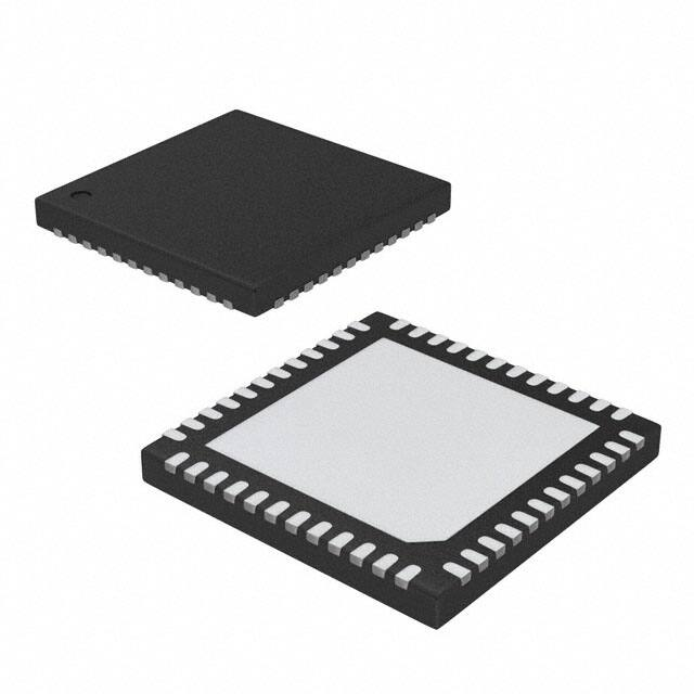


 工商网监
湘ICP备2023018690号
工商网监
湘ICP备2023018690号
