Click here to ask about the production status of specific part numbers.
MAX25301A/MAX25301B
1A Automotive Low-Noise LDO Linear
Regulator
General Description
Benefits and Features
The MAX25301A/B are low-noise automotive linear regulators that deliver up to 1A of output current with only
7µVRMS of output noise from 10Hz to 100kHz.
●
●
●
●
●
●
●
●
●
●
●
●
●
●
●
●
●
These regulators maintain ±1% output accuracy over a
wide input-voltage range, requiring only 100mV of inputto-output headroom at full load. The 1200µA no-load supply current is independent of dropout voltage.
The MAX25301A has nine pin-selectable output voltages:
1.2V, 1.5V, 1.8V, 2.5V, 3.0V, 3.1V, 3.3V, 4.0V, and 5V.
The MAX25301B output voltage can be adjusted to a value in the range of 0.6V to 5.3V using two external resistors. The MAX25301B also includes an active-high POK
signal for trouble-free load startup.
All versions include a programmable output soft-start rate
as well as output-overcurrent and thermal-overload protection.
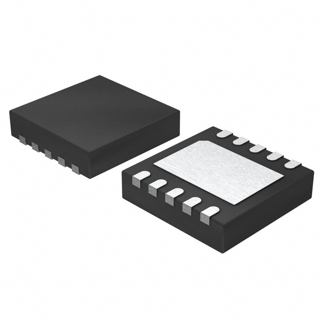
The MAX25301A/B are offered in a 10-pin TDFN (3mm x
3mm) package.
Applications
● Automotive Electronics
● Audio Systems
● High-Resolution Data Acquisition Systems
19-100783; Rev 0; 6/20
1.7V to 5.5V Input Voltage Range
0.6V to 5.3V Programmable Output Voltage
7µVRMS Output Noise, 10Hz to 100kHz
1200µA Operating Supply Current
70dB PSRR at 10kHz
1A Maximum Output Current
±1% DC Accuracy Over Load, Line, and Temperature
100mV Maximum Dropout at 1A Load
VOUT + 0.1V
Output Capacitance
COUT
For stability and proper operation
IQ
Supply Current
MIN
Guaranteed by output accuracy
4
IOUT = 0mA
1.6
MAX
UNITS
5.5
V
1.7
V
5.3
10
1200
2000
0.01
0.1
TJ = +125°C
0.1
VEN = 0V
Output Accuracy
(MAX25301A Only)
ACC25301A
IOUT from 0.1mA to 1A, VIN from VOUT +
0.3V to 5.5V, VIN > 1.7V
-1.0
Output Accuracy
(MAX25301B Only)
ACC25301B
IOUT from 0.1mA to 1A, VIN from VOUT +
0.3V to 5.5V, VIN > 1.7V
0.594
Load Regulation
IOUT from 0.1mA to 1A
Load Transient
IOUT = 50mA to 1A to 50mA, tRISE =
tFALL = 1µs
19-100783
0.6
V
µF
TJ = +25°C
ISHUTDOWN
www.maximintegrated.com
TYP
µA
μA
1.0
%
0.606
V
0.02
%/V
50
mV
Maxim Integrated | 5
�MAX25301A/MAX25301B
1A Automotive Low-Noise LDO Linear Regulator
Electrical Characteristics (continued)
(VIN = 3.6V, TJ = -40°C to +125°C, CBYP = 0.047μF, CIN = 10µF, COUT = 10µF, IOUT = 100mA, unless otherwise specified. Note 1.)
PARAMETER
SYMBOL
CONDITIONS
Line Regulation
VIN from VOUT + 0.3V to 5.5V, VIN >
1.7V
Line Transient
VIN = 4V to 5V to 4V, IOUT = 1A, tRISE =
tFALL = 5µs
Dropout Voltage (Note
2)
IOUT = 1A
Current Limit
VOUT = 95% of regulation
Output Noise
IOUT = 100mA, f =
10Hz to 100kHz
MIN
%/V
3
mV
50
100
80
160
150
300
1.4
1.6
1.15
CBYP = 47nF
7
f = 1kHz
70
f = 10kHz
70
f = 100kHz
60
PSRR
IOUT = 100mA
BYP Capacitor Range
CBYP
Regulator remains stable
f = 1MHz
VIN from 1.7V to
5.5V
EN falling
0.4
0.7
EN Input Leakage
Current
VEN from 1.7V to
5.5V
TJ = +25°C
-1
0.001
POK Threshold
(MAX25301B Only)
VOUT when POK
switches
VOUT rising
POK Voltage, Low
(MAX25301B Only)
IPOK = 1mA
POK Leakage Current
(MAX25301B Only)
VPOK = 5.5V
SELA/B Input
Capacitance
(MAX25301A Only)
CINSELA/B
dB
50
EN Input Threshold
0.8
TJ = +125°C
88
91
+1
94
88
-0.1
TJ = +125°C
10
100
0.001
+0.1
0.01
When shorted to GND or IN
500
1
10
VOUT = 3.6V, when VIN falls to 0V
Thermal Shutdown
Threshold
TJ when output
turns on/off
V
µA
%
mV
µA
Ω
MΩ
When Hi-Z
Input Reverse-Current
Threshold
µF
µA
1.2
0.01
VOUT falling
When Hi-Z
A
µVRMS
0.1
EN rising
RINSELA/B
mV
40
0.001
From BYP to GND during startup
TJ = +25°C
UNITS
0.05
VIN = 2.5V (Note 3)
Power Supply Rejection
Ratio
SELA/B Input
Resistance
(MAX25301A Only)
MAX
VIN = 3.6V
VIN = 1.7V
BYP Soft-Start Current
TYP
400
TJ rising
165
TJ falling
150
pF
mA
°C
Note 1: Limits over the specified operating temperature and supply voltage range are guaranteed by design and characterization, and
production tested at room temperature only.
Note 2: Dropout voltage is defined as (VIN - VOUT), when VIN = VOUT(NOMINAL) - 0.1V. For VOUT(NOMINAL) less than 1.7V, dropout
voltage is not guaranteed.
Note 3: Guaranteed by design and characterization.
www.maximintegrated.com
19-100783
Maxim Integrated | 6
�MAX25301A/MAX25301B
1A Automotive Low-Noise LDO Linear Regulator
Typical Operating Characteristics
(MAX25301B, VIN = 5.0V, VOUT = 3.3V, TA = 25°C, CIN = 10µF , COUT = 10µF, unless otherwise noted.)
www.maximintegrated.com
19-100783
Maxim Integrated | 7
�MAX25301A/MAX25301B
1A Automotive Low-Noise LDO Linear Regulator
Pin Configurations
MAX25301A
TOP VIEW (PAD-SIDE DOWN)
IN
1
10
OUT
IN
2
9
OUT
EXPOSED
PAD
GND
3
8
BYP
EN
4
7
OUTS
SELA
5
6
SELB
10-PIN TDFN 3mm x 3mm
www.maximintegrated.com
19-100783
Maxim Integrated | 8
�MAX25301A/MAX25301B
1A Automotive Low-Noise LDO Linear Regulator
MAX25301B
TOP VIEW (PAD-SIDE DOWN)
IN
1
10
OUT
IN
2
9
OUT
EXPOSED
PAD
GND
3
8
BYP
EN
4
7
FB
GS
5
6
POK
10-PIN TDFN 3mm x 3mm
Pin Description
PIN
NAME
FUNCTION
1, 2
IN
Regulator Supply Input. Connect to a voltage between 1.7V and 5.5V and bypass
with a 10µF capacitor from IN to GND.
3
3
GND
Regulator Ground. Connect IN and OUT bypass capacitor GND connections to
this pin for best performance.
4
4
EN
Enable Input. Connect this pin to a logic signal to enable (VEN high) or disable
(VEN low) the regulator output. Connect to IN to keep the output enabled
whenever a valid supply voltage is present.
5
---
SELA
Select Input A. Connect to GND, IN, or leave unconnected to select the output
voltage. This pin is read only at startup.
---
5
GS
6
---
SELB
Select Input B. Connect to GND, IN, or leave unconnected to select the output
voltage. This pin is read only at startup.
---
6
POK
Active-High Power-OK Output. Connect a pullup resistor from this pin to a supply
to create a reset signal that goes high after the regulator output has reached its
regulation voltage.
7
---
OUTS
MAX25301A
MAX25301B
1, 2
www.maximintegrated.com
Ground Sense. Connect GS to GND.
Output Voltage Sense Input. Connect to the load at a point where accurate
regulation is required to eliminate resistive metal drops.
19-100783
Maxim Integrated | 9
�MAX25301A/MAX25301B
1A Automotive Low-Noise LDO Linear Regulator
Pin Description (continued)
PIN
NAME
FUNCTION
MAX25301A
MAX25301B
---
7
FB
8
8
BYP
Bypass Capacitor Input. Connect a capacitor with a value from 0.001µF to 0.1µF
between OUT and BYP to reduce output noise and set the regulator soft-start rate.
9, 10
9, 10
OUT
Regulator Output. Sources up to 1A at the output regulation voltage. Bypass with
a 10µF (4µF minimum including voltage derating) low-ESR (


 工商网监
湘ICP备2023018690号
工商网监
湘ICP备2023018690号
