EVALUATION KIT AVAILABLE
MAX40007
General Description
The MAX40007 is a single operational amplifier that provides
a maximized ratio of gain bandwidth (GBW) to supply current
and is ideal for battery-powered applications such as portable
instrumentation, portable medical equipment, and wireless
handsets.
This CMOS op amp features an ultra-low supply current
of only 700nA (typ), ground-sensing inputs, and rail-torail outputs; operating from a single 1.7V to 5.5V supply,
allowing the amplifier to be powered by the same 1.8V,
2.5V, or 3.3V nominal supply that powers the microcontroller.
The MAX40007 amplifier is unity-gain stable with a 20kHz
GBW product.
The ultra-low supply current, low operating voltage, and
rail-to-rail output capabilities make this operational amplifier
ideal for use in single lithium ion (Li+), two-cell NiCd or
alkaline battery systems.
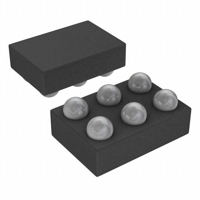
nanoPower Op Amp in Ultra-Tiny
WLP and SOT23 Packages
Benefits and Features
●● Ultra-Low-Power Preserves Battery Life
• 700nA Typical Supply Current
●● Single 1.7V to 5.5V Supply Voltage Range
• Amplifier Can be Powered From the Same
1.8V/2.5V/3.3V/5V System Rails
●● Tiny Packages Save Board Space
• 1.1mm x 0.76mm WLP-6 with 0.35mm Bump Pitch
• SOT23-6 Package
●● Precision Specifications for Buffer/Filter/Gain Stages
• Low 300μV Input Offset Voltage
• Rail-to-Rail Output Voltage
• 20kHz BW
• Low 40pA Input Bias Current
• Unity-Gain Stable
●● -40°C to 125°C Temperature Range
The MAX40007 is available in a 6-pin SOT23 package
and an ultra-tiny 6-bump, 1.1mm x 0.76mm wafer-level
package (WLP) with a bump pitch of 0.35mm. The
amplifier is specified over the -40°C to 125°C operating
temperature range.
Applications
●●
●●
●●
●●
●●
Fitness Wearables
Mobile Phones
Notebook and Tablet Computers
Portable Medical Devices
Portable Instrumentation
19-8735; Rev 1; 1/18
Ordering Information appears at end of data sheet.
�MAX40007
nanoPower Op Amp in Ultra-Tiny
WLP and SOT23 Packages
Absolute Maximum Ratings
VDD to VSS...............................................................-0.3V to +6V
IN+, IN- to VSS..................................... VSS -0.3V to VDD + 0.3V
IN+ to IN-............................................................................. ±VDD
OUT to VSS.......................................... VSS -0.3V to VDD + 0.3V
Continuous Current Into Any Input Pin..............................±10mA
Continuous Current Into Output Pin..................................±30mA
Output Short-Circuit Duration to VDD or VSS......................... 10s
Continuous Power Dissipation (TA = +70°C)
6-Bump WLP (derate 10.19mW/°C at 70°C)................816mW
SOT23-6 (derate 4.30mW/°C at 70°C)....................347.80mW
Operating Temperature Range.......................... -40°C to +125°C
Junction Temperature.......................................................+150°C
Storage Temperature Range............................. -65°C to +150°C
Lead Temperature (soldering, 10s).................................. +300°C
Soldering Temperature (reflow)........................................+260°C
Stresses beyond those listed under “Absolute Maximum Ratings” may cause permanent damage to the device. These are stress ratings only, and functional operation of the device at these
or any other conditions beyond those indicated in the operational sections of the specifications is not implied. Exposure to absolute maximum rating conditions for extended periods may affect
device reliability.
Package Thermal Characteristics (Note 1)
WLP
Junction-to-Ambient Thermal Resistance (θJA)......98.06°C/W
SOT23
Junction-to-Ambient Thermal Resistance (θJA).........230°C/W
Junction-to-Case Thermal Resistance (θJC)................76°C/W
Note 1: Package thermal resistances were obtained using the method described in JEDEC specification JESD51-7, using a four-layer
board. For detailed information on package thermal considerations, refer to www.maximintegrated.com/thermal-tutorial.
Electrical Characteristics
VDD = +3V, VSS = 0V, VCM = 0.5V, VOUT = VDD/2, RL = 1MΩ to VDD/2, TA = +25°C, unless otherwise noted. (Note 2)
PARAMETER
Supply Voltage Range
SYMBOL
VDD
CONDITIONS
Guaranteed by PSRR tests
MIN
TYP
1.7
MAX
UNITS
5.5
V
Supply Current
IDD
At 25°C
0.7
0.9
µA
Input Offset Voltage
VOS
VSS - 0.1V < CMIR < VDD - 1.1V
±0.3
±1.3
mV
IB
±40
±100
pA
IOS
±5
±50
pA
Input Bias Current (Note 3)
Input Offset Current
(Note 3)
Input Capacitance
Input Common-Mode
Voltage Range
Either input, over entire common mode range
VCM
Guaranteed by the CMRR test
DC, (VSS - 0.1) ≤ VCM ≤ (VDD - 1.1V)
1.5
VSS 0.1V
70
pF
VDD
-1.1
92
V
Common-Mode Rejection
Ratio
CMRR
Power-Supply Rejection
Ratio
PSRR
Large-Signal Voltage Gain
AVOL
RL = 1MΩ, VOUT = VSS + 25mV to
VDD - 25mV
VOH
Swing high specified as
VDD – VOUT
RL = 100kΩ
3.2
8
RL = 10kΩ
32
70
VOL
Swing low specified as
VOUT - VSS
RL = 100kΩ
2.9
8
RL = 10kΩ
27
70
GBW
AV = 1, CL = 20pF
15
kHz
CL = 20pF
56
°
Output Voltage Swing
Gain-Bandwidth Product
Phase Margin
www.maximintegrated.com
φM
AC, 100mVPP 1kHz, with output at VDD/2
DC, +1.7V ≤ VDD ≤ +5.5V
dB
72
75
AC, 100mVPP 1kHz, superimposed on VDD/2
100
dB
75
75
110
dB
mV
Maxim Integrated │ 2
�MAX40007
nanoPower Op Amp in Ultra-Tiny
WLP and SOT23 Packages
Electrical Characteristics (continued)
VDD = +3V, VSS = 0V, VCM = 0.5V, VOUT = VDD/2, RL = 1MΩ to VDD/2, TA = +25°C, unless otherwise noted. (Note 2)
PARAMETER
Slew Rate
SYMBOL
SR
Settling Time
CONDITIONS
MIN
TYP
MAX
UNITS
VOUT = 1VP-P step, AV = 1V/V
12
V/ms
100mV step, 0.1% settling, AV = 1
74
µs
Input Voltage Noise
en
f = 1kHz
513
nV/√Hz
Input Current Noise
in
f = 1kHz
0.004
pA/√Hz
Shorted to VSS (sourcing)
10
mA
Shorted to VDD (sinking)
10
mA
0.13
ms
20
pF
Output Short-Circuit
Current
Power-On Time
tON
Stable Capacitive Load
CL
No sustained oscillations
Electrical Characteristics
VDD = +3V, VSS = 0V, VCM = 0.5V, VOUT = VDD/2, RL = 1MΩ to VDD/2, TA = +40°C to +125°C, unless otherwise noted. (Note 2)
PARAMETER
Supply Voltage Range
SYMBOL
VDD
Supply Current
IDD
Input Offset Voltage
VOS
Input Offset Voltage
Temperature Coefficient
Input Bias Current
(Note 3)
Input Common-Mode
Voltage Range
CONDITIONS
Guaranteed by PSRR tests
MIN
TYP
1.7
MAX
UNITS
5.5
V
TA = -40°C to 85°C
1.2
TA = -40°C to 125°C
1.4
TA = -40°C to 125°C
±4.5
mV
µA
TCVOS
6.4
36.6
µV/°C
IB
0.7
7
nA
VDD
-1.1
V
VCM
Guaranteed by the CMRR test
VSS 0.1
Common-Mode Rejection
Ratio
CMRR
DC, (VSS - 0.1) ≤ VCM ≤ (VDD - 1.1V)
AC, 100mVP-P 1kHz, with output at VDD/2
70
Power-Supply Rejection
Ratio
PSRR
+1.7V ≤ VDD ≤ +5.5V, -40°C ≤ TA ≤ +125°C
AC, 100mVP-P 1kHz, superimposed on VDD
75
Large-Signal Voltage Gain
AVOL
VOUT = 50mV to VDD - 50mV, RL = 1MΩ
75
VOH
Swing high specified as
VDD - VOUT
RL = 100kΩ
8
RL = 10kΩ
70
VOL
Swing low specified as
VOUT - VSS
RL = 100kΩ
8
RL = 10kΩ
70
Output Voltage Swing
63
40
dB
dB
dB
mV
Note 2: All devices are production tested at TA = +25°C. All temperature limits are guaranteed by design.
Note 3: Guaranteed by design and bench characterization.
www.maximintegrated.com
Maxim Integrated │ 3
�MAX40007
nanoPower Op Amp in Ultra-Tiny
WLP and SOT23 Packages
Typical Operating Characteristics
(VDD = +3V, VSS = 0V, VCM = 0V, RL = 100kΩ to VDD/2, TA = +25°C, unless otherwise noted.)
SUPPLY CURRENT
vs. TEMPERATURE
SUPPLY CURRENT vs. SUPPLY VOLTAGE
toc01
QUIESCENT SUPPLY CURRENT (μ A)
1.8
1.6
TA = 125°C
1.4
1.2
TA = 85°C
1
0.8
0.6
0.4
TA = -40°C
0.2
toc02
1200
QUIESCENT SUPPLY CURRENT (nA)
2
1000
VDD = 3.3V
800
600
400
200
TA = 25°C
0
0
-40 -25 -10 5
0 0.5 1 1.5 2 2.5 3 3.5 4 4.5 5 5.5
INPUT BIAS CURRENTS vs.
INPUT COMMON MODE VOLTAGE
INPUT BIAS CURRENTS vs. TEMPERATURE
200
toc03
VDD = 3.0V
VDD = 3.0V
10
INPUT BIAS CURRENT (pA)
INPUT BIAS CURRENT (pA)
toc04
15
IB-
0
-200
-400
IB+
-600
-800
IB-
5
0
-5
-1000
-1200
IB+
-10
-40 -25 -10 5
20 35 50 65 80 95 110 125
0
0.5
TEMPERATURE (°C)
2
98
-30
96
-40
VDD = 5.5V
THD + N (dB)
-20
VDD = 3.0V
toc06
-10
100
92
1.5
TOTAL HARMONIC DISTORTIONPLUS NOISE
vs. FREQUENCY
toc05
102
94
1
INPUT COMMON MODE VOLTAGE (V)
DC CMRR vs. TEMPERATURE
DC CMRR (dB)
20 35 50 65 80 95 110 125
TEMPERATURE(°C)
SUPPLY VOLTAGE (V)
VOUT = 1.5 VPP
-50
-60
90
-70
88
-80
-90
86
-40 -25 -10 5
20 35 50 65 80 95 110 125
TEMPERATURE (°C)
www.maximintegrated.com
10
100
1000
10000
100000
FREQUENCY(kHz)
Maxim Integrated │ 4
�MAX40007
nanoPower Op Amp in Ultra-Tiny
WLP and SOT23 Packages
Typical Operating Characteristics (continued)
(VDD = +3V, VSS = 0V, VCM = 0V, RL = 100kΩ to VDD/2, TA = +25°C, unless otherwise noted.)
VOLTAGENOISE DENSITY vs. FREQUENCY
toc07
NOISE SPECTRAL DENSITY (µV/√Hz)
12
9
6
3
0
0.1
10
1000
100000
FREQUENCY(Hz)
www.maximintegrated.com
Maxim Integrated │ 5
�MAX40007
nanoPower Op Amp in Ultra-Tiny
WLP and SOT23 Packages
Typical Operating Characteristics (continued)
(VDD = +3V, VSS = 0V, VCM = 0V, RL = 100kΩ to VDD/2, TA = +25°C, unless otherwise noted.)
SMALL SIGNAL GAIN
vs. FREQUENCY
SMALL SIGNAL GAIN
vs. FREQUENCY
toc13
20
15
AVCL = 1V/V
VOUT = 100mVP-P
CLOAD = 10pF,RL = 1MΩ
15
10
GAIN (dB)
GAIN (dB)
10
toc14
20
AVCL = 1V/V
VOUT = 100mVP-P
CL = 10pF, RL = 100KΩ
5
0
5
0
-5
-5
-10
-10
-15
-15
-20
0.01
0.1
1
10
Frequency (kHz)
100
-20
1000
0.01
Thousands
0.1
LARGE SIGNAL GAIN
vs. FREQUENCY
1000
Thousands
AVCL = 1V/V
VOUT = 1VP-P
CL = 10pF, RL = 1MΩ
15
10
GAIN (dB)
10
GAIN (dB)
100
toc16
20
AVCL = 1V/V
VOUT = 1VP-P
CL = 10pF, RL = 100KΩ
15
10
LARGE SIGNAL GAIN
vs. FREQUENCY
toc15
20
1
Frequency (kHz)
5
0
5
0
-5
-5
-10
-10
-15
-15
-20
-20
0.01
0.1
1
10
Frequency (kHz)
www.maximintegrated.com
100
1000
Thousands
0.01
0.1
1
10
Frequency (kHz)
100
1000
Thousands
Maxim Integrated │ 6
�MAX40007
nanoPower Op Amp in Ultra-Tiny
WLP and SOT23 Packages
Pin Configurations
(TOP VIEW)
(TOP VIEW)
2
3
A
IN+
IN-
OUT
B
NC
VDD
VSS
OUT
1
VSS
2
IN+
3
+
6 VDD
+
1
MAX40007
6-WLP
MAX40007
5 NC
4 IN-
SOT23-6
Pin Description
BUMP (WLP)
6-SOT23
NAME
A1
3
IN+
Non-Inverting Amplifier Input.
A2
4
IN-
Inverting Amplifier Input.
A3
1
OUT
B1
5
NC
No Connection. Internally connected.
B2
6
VDD
Positive Power Supply Input.
B3
2
VSS
Negative Power Supply Input. Connect VSS to 0V in single-supply application.
www.maximintegrated.com
FUNCTION
Amplifier Output.
Maxim Integrated │ 7
�MAX40007
nanoPower Op Amp in Ultra-Tiny
WLP and SOT23 Packages
Functional (or Block) Diagram
VDD
IN-
12.5kΩ
OUT
MAX40007
IN+
12.5kΩ
NC
VSS
Detailed Description
The MAX40007 is an ultra-low-power op amp ideal for
battery-powered applications and features a maximized
ratio of GBW to supply current, low operating supply voltage,
and low input bias current. The MAX40007 is ideal for
general-purpose, low-current, low-voltage continuously
powered portable applications. The MAX40007 consumes
an ultra-low 700nA (typ) supply current and has a 0.3mV
(typ) offset voltage. This device is unity-gain stable with a
20kHz GBW product, driving capacitive loads up to 20pF.
Applications Information
Ground Sensing
The common-mode input range of the MAX40007 extends
down to VSS, and offers excellent common-mode rejection.
This op amp is guaranteed not to exhibit phase reversal
when either input is overdriven.
Power Supplies and Layout
The MAX40007 operates from a single +1.7V to +5.5V
power supply. Bypass the power supplies with a 0.1μF
ceramic capacitor placed close to VDD and VSS pins.
Adding a solid Ground plane improves performance
generally by decreasing the noise at the op amp’s inputs
However, in very high impedance circuits, it may be worth
removing the ground plane under the IN- pin to reduce the
stray capacitance and help avoid reducing the phase margin. To further decrease stray capacitance, minimize PCB
lengths and resistor leads, and place external components
close to the amplifier’s pins.
www.maximintegrated.com
Input Differential Voltage Protection
The MAX40007’s inputs are protected from large differential
voltages by the network shown in Figure 1. This is done
to prevent gradual degradation of the input offset voltage.
In normal operation, the amplifier inputs are at almost
the same voltage at all times so these components are
transparent to normal operation. Using this amplifier as
a comparator, however, is not recommended—the inputs
will start to draw “bias current’ when the differential voltage
exceeds about 1V. While this will not damage the
amplifier in any way, it is not usually a desirable feature for
a comparator. Maxim does make comparators with similar
speed and power performance as these amplifiers, such
as the MAX40002/3/4/5.
IN-
12.5kΩ
MAX40007
OUT
IN+
12.5kΩ
Figure 1. Input Protection Scheme
Maxim Integrated │ 8
�MAX40007
nanoPower Op Amp in Ultra-Tiny
WLP and SOT23 Packages
Stability
This MAX40007 maintains stability in its minimum gain configuration while driving capacitive loads up to 20pF or so.
Larger capacitive loading is achieved using the techniques
described in the Capacitive Load Stability section below.
Although this amplifier is primarily designed for lowfrequency applications, good layout can still be extremely
important, especially if very high-value resistors are being
used—as is likely in ultra-low-power circuitry. However,
some stray capacitance may be unavoidable; and it may
be necessary to add a 2pF to 10pF capacitor across the
feedback resistor, as shown in Figure 2. Select the smallest
capacitor value that ensures stability so that BW and
settling time are not significantly impacted.
Capacitive Load Stability
Driving large capacitive loads can cause instability in
amplifiers. The MAX40007 is stable with capacitive loads
up to 20pF. Stability with higher capacitive loads can be
achieved by adding an isolation resistor in series with the
op-amp output as shown in Figure 2 below. This resistor
improves the circuit’s phase margin by isolating the load
capacitor from the amplifier’s inverting input. The graph in
the Typical Operating Characteristics gives the stable operation
region for capacitive load versus isolation resistors.
VDD
IN+
VDD
MAX40007
OUT
IN+
IN-
MAX40007
OUT
RISO
IN-
VSS
R1
CL
RL
VSS
R2
2pF TO 10pF
Figure 2. Compensation for Feedback Node Capacitance
Figure 3. RISO Improving Capacitive Load Drive Capability of
Op Amp
Ordering Information
Package Information
PART
TEMP
RANGE
PIN
PACKAGE
TOP
MARK
MAX40007ANT+
-40°C to +125°C
6-WLP
+2
MAX40007AUT+
-40°C to +125°C
6-SOT23
+ACUV
+Denotes a lead(Pb)-free/RoHS-compliant package.
Chip Information
PROCESS: BiCMOS
www.maximintegrated.com
For the latest package outline information and land patterns
(footprints), go to www.maximintegrated.com/packages. Note
that a “+”, “#”, or “-” in the package code indicates RoHS status
only. Package drawings may show a different suffix character, but
the drawing pertains to the package regardless of RoHS status.
PACKAGE
TYPE
PACKAGE
CODE
OUTLINE
NO.
LAND
PATTERN NO.
6-WLP
N60D1+1
21-100086
Refer to
Application
Note 1891
6-SOT23
U6+1
21-0058
90-0175
Maxim Integrated │ 9
�MAX40007
nanoPower Op Amp in Ultra-Tiny
WLP and SOT23 Packages
Revision History
REVISION
NUMBER
REVISION
DATE
0
12/16
Initial release
—
1
1/18
Updated Ordering Informaiton table
9
DESCRIPTION
PAGES
CHANGED
For pricing, delivery, and ordering information, please contact Maxim Direct at 1-888-629-4642, or visit Maxim Integrated’s website at www.maximintegrated.com.
Maxim Integrated cannot assume responsibility for use of any circuitry other than circuitry entirely embodied in a Maxim Integrated product. No circuit patent licenses
are implied. Maxim Integrated reserves the right to change the circuitry and specifications without notice at any time. The parametric values (min and max limits)
shown in the Electrical Characteristics table are guaranteed. Other parametric values quoted in this data sheet are provided for guidance.
Maxim Integrated and the Maxim Integrated logo are trademarks of Maxim Integrated Products, Inc.
© 2018 Maxim Integrated Products, Inc. │ 10
�