19-2330; Rev 0; 1/02
Single-Supply 3V/5V, Voltage-Output, Dual,
Precision 12-Bit DACs
Features
♦ Guaranteed 1/2LSB INL (max)
The MAX5234/MAX5235 are fully specified over the
extended industrial temperature range (-40°C to +85°C)
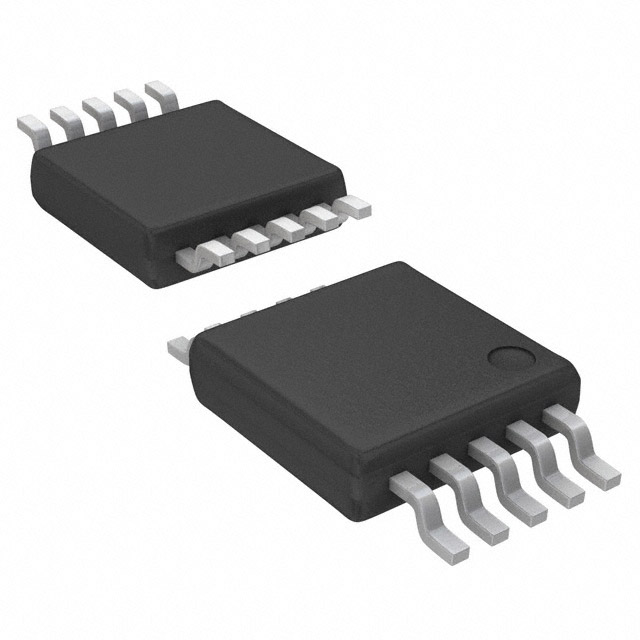
and are available in space-saving 10-pin µMAX packages.
♦ Programmable Shutdown Modes with 1kΩ or
200kΩ Internal Loads
Applications
Industrial Process Controls
♦ Low Supply Current
325µA (Normal Operation)
0.4µA (Full Power-Down Mode)
♦ Single-Supply Operation
3V (MAX5234)
5V (MAX5235)
♦ Space-Saving 10-Pin µMAX Package
♦ Output Buffers Swing Rail-to-Rail
♦ Power-On Reset Clears Registers and DACs
to Zero
♦ Resets to Zero
♦ 13.5MHz SPI/QSPI/MICROWIRE-Compatible,
3-Wire Serial Interface
♦ Buffered Output Drives 5kΩ || 100pF
Automatic Test Equipment
Digital Offset and Gain Adjustment
Ordering Information
Motion Control
µP-Controlled Systems
PART
TEMP
RANGE
PINPACKAGE
INL
(LSB)
±0.5
MAX5234AEUB
-40°C to +85°C
10 µMAX
MAX5234BEUB
-40°C to +85°C
10 µMAX
±1
MAX5235AEUB
-40°C to +85°C
10 µMAX
±0.5
MAX5235BEUB
-40°C to +85°C
10 µMAX
±1
Pin Configuration
TOP VIEW
OUTA 1
Rail-to-Rail is a registered trademark of Nippon Motorola, Ltd.
REFA
2
GND
3
LDAC
CS
10 OUTB
9
REFB
8
VDD
4
7
DIN
5
6
SCLK
MAX5234
MAX5235
SPI/QSPI are trademarks of Motorola, Inc.
MICROWIRE is a trademark of National Semiconductor Corp.
µMAX
________________________________________________________________ Maxim Integrated Products
For pricing, delivery, and ordering information, please contact Maxim/Dallas Direct! at
1-888-629-4642, or visit Maxim’s website at www.maxim-ic.com.
1
MAX5234/MAX5235
General Description
The MAX5234/MAX5235 precision, dual-output, 12-bit
digital-to-analog converters (DACs) consume only 360µA
from a single 5V (MAX5235) or 325µA from a single 3V
(MAX5234) supply. These devices feature output buffers
that swing Rail-to-Rail®. The internal gain amplifiers maximize the dynamic range of the DAC output.
The MAX5234/MAX5235 feature a 13.5MHz 3-wire serial interface compatible with SPI™, QSPI™, and
MICROWIRE™. Each DAC input is organized as an
input register followed by a DAC register. A 16-bit shift
register loads data into the input registers. Input registers update the DAC registers independently or simultaneously. In addition, programmable control bits allow
power-down with 1kΩ or 200kΩ internal loads.
�MAX5234/MAX5235
Single-Supply 3V/5V, Voltage-Output, Dual,
Precision 12-Bit DACs
ABSOLUTE MAXIMUM RATINGS
VDD to GND .............................................................-0.3V to +6V
Digital Inputs to GND ..............................................-0.3V to +6V
REF_, OUT_ to GND ................................-0.3V to (VDD + 0.3V)
Maximum Current into Any Pin............................................50mA
Continuous Power Dissipation (TA = +70°C)
10-Pin µMAX (derate 5.60mW/°C above +70°C) .........444mW
Operating Temperature Range ...........................-40°C to +85°C
Storage Temperature Range .............................-65°C to +150°C
Lead Temperature (soldering, 10s) .................................+300°C
Stresses beyond those listed under “Absolute Maximum Ratings” may cause permanent damage to the device. These are stress ratings only, and functional
operation of the device at these or any other conditions beyond those indicated in the operational sections of the specifications is not implied. Exposure to
absolute maximum rating conditions for extended periods may affect device reliability.
ELECTRICAL CHARACTERISTICS—MAX5235
(VDD = +4.5V to +5.5V, GND = 0, VREFA = VREFB = +2.5V, RL= 5kΩ, CL = 100pF, TA = TMIN to TMAX, unless otherwise noted. Typical
values are at TA = +25°C.)
PARAMETER
SYMBOL
CONDITIONS
MIN
TYP
MAX
UNITS
STATIC PERFORMANCE
Resolution
N
Integral Nonlinearity
INL
Differential Nonlinearity
DNL
Offset Error
VOS
12
Bits
MAX5235A (Note 1)
±0.5
MAX5235B (Note 1)
±1
±1
(Note 2)
Gain Error
Full-Scale Voltage
VFS
Full-Scale Temperature
Coefficient
TCVFS
Offset Temperature Coefficient
TCVOS
Power-Supply Rejection
PSR
DC Crosstalk
Code = FFF hex, TA = +25°C (Note 3)
4.087
Normalized to 4.095V
4.5V ≤ VDD ≤ 5.5V
4.095
LSB
LSB
±5
mV
±3
LSB
4.103
V
2
ppm/°C
±8
µV/°C
15
(Note 4)
200
µV
100
µV
REFERENCE INPUT
Reference Input Range
VREF
(Note 5)
Reference Input Resistance
RREF
Minimum with code 555 hex and AAA hex
Reference Current in Shutdown
IREF
0.25
28
2.60
37
V
kΩ
±1
µA
MULTIPLYING MODE PERFORMANCE
Reference -3dB Bandwidth,
Slew-Rate Limited
Input code = FFF hex, VREF_ = 0.5VP-P +
1.5VDC
350
kHz
Reference Feedthrough
Input code = 000 hex, VREF_ = 3.6VP-P +
1.8VDC, f = 1kHz
-80
dB
Input code = FFF hex, VREF_ = 2VP-P +
1.5VDC, f = 10kHz
79
dB
Signal-to-Noise plus Distortion
Ratio
2
SINAD
_______________________________________________________________________________________
�Single-Supply 3V/5V, Voltage-Output, Dual,
Precision 12-Bit DACs
(VDD = +4.5V to +5.5V, GND = 0, VREFA = VREFB = +2.5V, RL= 5kΩ, CL = 100pF, TA = TMIN to TMAX, unless otherwise noted. Typical
values are at TA = +25°C.)
PARAMETER
SYMBOL
CONDITIONS
MIN
TYP
MAX
UNITS
DIGITAL INPUT
Input High Voltage
VIH
Input Low Voltage
VIL
Input Hysteresis
0.7 x
VDD
0.3 x
VDD
VHYS
Input Leakage Current
V
200
mV
±1
Digital inputs = 0 or VDD
Input Capacitance
V
µA
8
pF
0.6
V/µs
10
µs
0 to
VDD
V
DYNAMIC PERFORMANCE
Voltage-Output Slew Rate
SR
Voltage-Output Settling Time
To ±0.5LSB, VSTEP = ±4V,
0.25V < VOUT < (VDD - 0.25V)
Output-Voltage Swing
(Note 6)
Time Required for Output to Settle
After Turning on VDD
(Note 7)
70
µs
Time Required for Output to
Settle After Exiting Full PowerDown
(Note 7)
70
µs
Time Required for Output to
Settle After Exiting DAC PowerDown
(Note 7)
60
µs
Digital Feedthrough
CS = VDD, fSCLK = 100kHz, VSCLK = 5VP-P
Major-Carry Glitch Energy
5
nV-s
40
nV-s
POWER SUPPLIES
Power-Supply Voltage
VDD
Power-Supply Current
IDD
Power-Supply Current in PowerDown and Shutdown Modes
ISHDN
4.5
5.5
V
(Note 8)
360
450
µA
Full power-down mode
One DAC shutdown mode
Both DACs shutdown mode
1
190
26
5
215
42
µA
_______________________________________________________________________________________
3
MAX5234/MAX5235
ELECTRICAL CHARACTERISTICS—MAX5235 (continued)
�MAX5234/MAX5235
Single-Supply 3V/5V, Voltage-Output, Dual,
Precision 12-Bit DACs
ELECTRICAL CHARACTERISTICS—MAX5234
(VDD = +2.7V to +3.6V, GND = 0, VREFA = VREFB = +1.25V, RL = 5kΩ, CL = 100pF, TA = TMIN to TMAX, unless otherwise noted.
Typical values are at TA = +25°C.)
PARAMETER
SYMBOL
CONDITIONS
MIN
TYP
MAX
UNITS
STATIC PERFORMANCE
Resolution
N
Integral Nonlinearity
INL
Differential Nonlinearity
DNL
Offset Error
VOS
Gain Error
GE
Full-Scale Voltage
VFS
Temperature Coefficient
TCVFS
Offset Temperature Coefficient
TCVOS
Power-Supply Rejection
PSR
DC Crosstalk
12
Bits
MAX5234A (Note 1)
±0.5
MAX5234B (Note 1)
±1
±1
(Note 2)
Code = FFF hex, TA = +25°C (Note 3)
2.041
Normalized to 2.0475V
2.7V ≤ VDD ≤ 3.6V
2.0475
LSB
LSB
±5
mV
±6
LSB
2.054
V
4
ppm/°C
±8
µV/°C
18
(Note 4)
280
µV
100
µV
REFERENCE INPUT
Reference Input Range
VREF
(Note 5)
Reference Input Resistance
RREF
Minimum with code 555 hex and AAA hex
Reference Current in Shutdown
IREF
0.25
28
1.50
37
V
kΩ
±1
µA
MULTIPLYING MODE PERFORMANCE
Reference -3dB Bandwidth, SlewRate Limited
Input code = FFF hex, VREF_ = 0.5VP-P +
0.75VDC
350
kHz
Reference Feedthrough
Input code = 000 hex, VREF_ = 1.6VP-P +
0.8VDC, f = 1kHz
-80
dB
Input code = FFF hex, VREF_ = 0.6VP-P +
0.9VDC, f = 10kHz
79
dB
Signal-to-Noise plus Distortion
Ratio
SINAD
DIGITAL INPUTS
Input High Voltage
VIH
Input Low Voltage
VIL
Input Hysteresis
0.7 x
VDD
0.3 x
VDD
VHYS
Input Leakage Current
V
200
mV
±1
Digital inputs = 0 or VDD
Input Capacitance
V
µA
8
pF
0.6
V/µs
10
µs
0 to
VDD
V
DYNAMIC PERFORMANCE
Voltage-Output Slew Rate
SR
Voltage-Output Settling Time
To ±0.5LSB, VSTEP = ±2V,
0.25V < VOUT < (VDD - 0.25V)
Output-Voltage Swing
(Note 6)
4
_______________________________________________________________________________________
�Single-Supply 3V/5V, Voltage-Output, Dual,
Precision 12-Bit DACs
(VDD = +2.7V to +3.6V, GND = 0, VREFA = VREFB = +1.25V, RL = 5kΩ, CL = 100pF, TA = TMIN to TMAX, unless otherwise noted.
Typical values are at TA = +25°C.)
PARAMETER
SYMBOL
CONDITIONS
MIN
TYP
MAX
UNITS
Time Required for Output to Settle
After Turning on VDD
(Note 7)
60
µs
Time Required for Output to
Settle After Exiting Full PowerDown
(Note 7)
60
µs
Time Required for Output to
Settle After Exiting DAC PowerDown
(Note 7)
50
µs
Digital Feedthrough
CS = VDD, fSCLK = 100kHz, VSCLK = 3VP-P
Major Carry Glitch Energy
5
nV-s
115
nV-s
POWER SUPPLIES
Power-Supply Voltage
VDD
Power-Supply Current
IDD
Power-Supply Current in PowerDown and Shutdown Modes
ISHDN
2.7
3.6
V
µA
(Note 8)
325
430
Full power-down mode
0.4
5
One DAC shutdown mode
175
200
Both DACs shutdown mode
25
40
µA
TIMING CHARACTERISTICS—MAX5235 (FIGURES 1 AND 2)
(VDD = +4.5V to +5.5V, GND = 0, TA = TMIN to TMAX, unless otherwise noted. Typical values are at TA = +25°C.)
PARAMETER
SYMBOL
CONDITIONS
MIN
TYP
MAX
UNITS
SCLK Clock Period
tCP
74
ns
SCLK Pulse Width High
tCH
30
ns
ns
SCLK Pulse Width Low
tCL
30
CS Fall to SCLK Rise Setup Time
tCSS
30
ns
SCLK Rise to CS Rise Hold Time
tCSH
0
ns
DIN Setup Time
tDS
30
ns
DIN Hold Time
tDH
0
ns
SCLK Rise to CS Fall Delay
tCS0
10
ns
CS Rise to SCLK Rise Hold Time
tCS1
30
ns
CS Pulse Width High
tCSW
75
ns
LDAC Pulse Width Low
tLDL
30
ns
40
ns
CS Rise to LDAC Rise Hold Time
tCSLD
(Note 9)
_______________________________________________________________________________________
5
MAX5234/MAX5235
ELECTRICAL CHARACTERISTICS—MAX5234 (continued)
�MAX5234/MAX5235
Single-Supply 3V/5V, Voltage-Output, Dual,
Precision 12-Bit DACs
TIMING CHARACTERISTICS—MAX5234 (FIGURES 1 AND 2)
(VDD = +2.7V to +3.6V, GND = 0, TA = TMIN to TMAX, unless otherwise noted. Typical values are at TA = +25°C.)
PARAMETER
SYMBOL
CONDITIONS
MIN
TYP
MAX
UNITS
SCLK Clock Period
tCP
74
ns
SCLK Pulse Width High
tCH
30
ns
SCLK Pulse Width Low
tCL
30
ns
CS Fall to SCLK Rise Setup Time
tCSS
30
ns
SCLK Rise to CS Rise Hold Time
ns
tCSH
0
DIN Setup Time
tDS
30
ns
DIN Hold Time
tDH
0
ns
SCLK Rise to CS Fall Delay
tCS0
10
ns
CS Rise to SCLK Rise Hold Time
tCS1
30
ns
CS Pulse Width High
tCSW
75
ns
30
ns
75
ns
LDAC Pulse Width Low
tLDL
CS Rise to LDAC Rise Hold Time
tCSLD
(Note 9)
Note 1: Accuracy is guaranteed in the following way:
VDD
VREF_
ACCURACY GUARANTEED FROM CODE
TO CODE
3
1.250
20
4095
5
2.500
10
4095
Note 2: Offset is measured at the code closest to 10mV.
Note 3: Gain from VREF_ to VOUT_ is typically 1.638 x CODE/4096.
Note 4: DC crosstalk is measured as follows: set DAC A to midscale, and DAC B to zero, and measure DAC A output; then change
DAC B to full scale and measure ∆VOUT for DAC A. Repeat the same measurement with DAC A and DAC B interchanged.
DC crosstalk is the maximum ∆VOUT measured.
Note 5: The DAC output voltage is derived by gaining up VREF by 1.638 x CODE/4096. This gain factor may cause VOUT to try to
exceed the supplies. The maximum value of VREF in the reference input range spec prevents this from happening at full
scale. The minimum VREF value of 0.25V is determined by linearity constraints, not DAC functionality.
Note 6: Accuracy is better than 1LSB for VOUT = 10mV to VDD - 180mV.
Note 7: Guaranteed by design. Not production tested.
Note 8: RLOAD = ∞ and digital inputs are at either VDD or GND. VOUT = full-scale output voltage.
Note 9: This timing requirement applies only to CS rising edges, which execute commands modifying the DAC input register contents.
6
_______________________________________________________________________________________
�Single-Supply 3V/5V, Voltage-Output, Dual,
Precision 12-Bit DACs
INTEGRAL NONLINEARITY
vs. DIGITAL CODE (MAX5235)
0.20
0.15
0.10
0.1
0.05
0
-0.1
-0.3
-0.15
-0.4
-0.20
-0.5
-0.25
0.1
0
-0.1
-0.2
-0.3
-0.4
0
500 1000 1500 2000 2500 3000 3500 4000
500 1000 1500 2000 2500 3000 3500 4000
0
500 1000 1500 2000 2500 3000 3500 4000
DIGITAL INPUT CODE
DIGITAL INPUT CODE
DIGITAL INPUT CODE
DIFFERENTIAL NONLINEARITY
vs. DIGITAL INPUT CODE (MAX5235)
MAX5234
SUPPLY CURRENT vs. TEMPERATURE
MAX5235
SUPPLY CURRENT vs. TEMPERATURE
0.10
0.05
0
-0.05
-0.10
300
250
200
150
350
100
-0.15
300
250
200
150
100
50
-0.20
MAX5234 toc06
350
SUPPLY CURRENT (µA)
0.15
400
SUPPLY CURRENT (µA)
0.20
MAX5234 toc05
400
MAX5234 toc04
0.25
50
NO LOAD
-0.25
0
NO LOAD
0
500 1000 1500 2000 2500 3000 3500 4000
0
-40
-15
10
35
60
85
-40
-15
10
35
60
85
DIGITAL INPUT CODE
TEMPERATURE (°C)
TEMPERATURE (°C)
MAX5234
SUPPLY CURRENT vs. SUPPLY VOLTAGE
MAX5235
SUPPLY CURRENT vs. SUPPLY VOLTAGE
MAX5234
FULL POWER-DOWN SUPPLY CURRENT
vs. TEMPERATURE
SUPPLY CURRENT (µA)
300
250
200
150
300
250
200
150
100
100
50
50
2.8
2.9
3.0
3.1
SUPPLY VOLTAGE (V)
3.2
3.3
0.40
0.35
0.30
0.25
0.20
0.15
0.10
NO LOAD
0
0
2.7
0.45
0.05
NO LOAD
NO LOAD
0
MAX5234 toc09
350
SUPPLY CURRENT (µA)
350
0.50
MAX5234 toc08
400
MAX5234 toc07
400
SUPPLY CURRENT (µA)
0
-0.10
0
0.2
-0.05
-0.2
0.3
DNL (LSB)
0.2
INL (LSB)
INL (LSB)
0.3
0.4
MAX5234 toc02
0.4
DNL (LSB)
0.25
MAX5234 toc01
0.5
DIFFERENTIAL NONLINEARITY
vs. DIGITAL INPUT CODE (MAX5234)
MAX5234 toc03
INTEGRAL NONLINEARITY vs. DIGITAL
INPUT CODE (MAX5234)
4.5 4.6 4.7 4.8 4.9 5.0 5.1 5.2 5.3 5.4 5.5
SUPPLY VOLTAGE (V)
-40
-15
10
35
60
85
TEMPERATURE (°C)
_______________________________________________________________________________________
7
MAX5234/MAX5235
Typical Operating Characteristics
(VDD = +5V (MAX5235) VDD = +3V (MAX5234), RL = 5kΩ, CL = 100pF, VREF = +1.25V (MAX5234), VREF = +2.5V (MAX5235), CREF
= 0.1µF ceramic || 2.2µF electrolytic, both DACs on, VOUT = full scale, TA = +25°C, unless otherwise noted.)
�Typical Operating Characteristics (continued)
(VDD = +5V (MAX5235) VDD = +3V (MAX5234), RL = 5kΩ, CL = 100pF, VREF = +1.25V (MAX5234), VREF = +2.5V (MAX5235), CREF
= 0.1µF ceramic || 2.2µF electrolytic, both DACs on, VOUT = full scale, TA = +25°C, unless otherwise noted.)
178
25
24
23
177
0.8
176
175
174
173
0.7
0.6
0.5
0.4
0.3
22
172
0.2
21
171
0.1
NO LOAD
60
85
-40
TEMPERATURE (°C)
MAX5235
BOTH DACs SHUTDOWN SUPPLY
CURRENT vs. TEMPERATURE
MAX5235
ONE DAC SHUTDOWN SUPPLY CURRENT
vs. TEMPERATURE
180
170
SUPPLY CURRENT (µA)
27
26
25
24
23
85
4.0955
4.0950
4.0945
4.0940
4.0935
2.0454
2.0452
NO LOAD
-15
2.0449
10
35
TEMPERATURE (°C)
60
85
-40
MAX5234
FULL-SCALE ERROR vs. RESISTIVE LOAD
2.00
1.75
FULL-SCALE ERROR (LSB)
4.0960
2.0455
2.0450
NO LOAD
-40
MAX5234 toc16
4.0965
85
2.0451
120
MAX5235
FULL-SCALE OUTPUT vs. TEMPERATURE
4.0970
60
2.0453
90
60
10
35
TEMPERATURE (°C)
130
110
10
35
TEMPERATURE (°C)
-15
MAX5234
FULL-SCALE OUTPUT vs. TEMPERATURE
140
100
-15
-40
160
22
NO LOAD
85
150
21
-40
60
190
MAX5234 toc13
28
NO LOAD
0
10
35
TEMPERATURE (°C)
29
-15
VOUT (V)
35
30
20
NO LOAD
170
10
1.50
1.25
1.00
0.75
0.50
0.25
-15
10
35
TEMPERATURE (°C)
60
85
MAX5235
FULL-SCALE ERROR vs. RESISTIVE LOAD
4.0
3.5
FULL-SCALE ERROR (LSB)
-15
MAX5234 toc14
-40
MAX5234 toc17
20
MAX5234 toc18
26
0.9
SUPPLY CURRENT (µA)
27
1.0
MAX5234 toc12
179
SUPPLY CURRENT (µA)
SUPPLY CURRENT (µA)
28
MAX5235
FULL POWER-DOWN SUPPLY CURRENT
vs. TEMPERATURE
MAX5234 toc11
29
SUPPLY CURRENT (µA)
180
MAX5234 toc10
30
MAX5234
ONE DAC SHUTDOWN SUPPLY CURRENT
vs. TEMPERATURE
MAX5234 toc15
MAX5234
BOTH DACs SHUTDOWN SUPPLY
CURRENT vs. TEMPERATURE
VOUT (V)
MAX5234/MAX5235
Single-Supply 3V/5V, Voltage-Output, Dual,
Precision 12-Bit DACs
3.0
2.5
2.0
1.5
1.0
0.5
NO LOAD
4.0930
0
-40
8
-15
10
35
TEMPERATURE (°C)
60
85
0
2.5 3.0 3.5 4.0 4.5 5.0 5.5 6.0 6.5 7.0 7.5
RL (kΩ)
2.5 3.0 3.5 4.0 4.5 5.0 5.5 6.0 6.5 7.0 7.5
RL (kΩ)
_______________________________________________________________________________________
�Single-Supply 3V/5V, Voltage-Output, Dual,
Precision 12-Bit DACs
MAX5234
DYNAMIC RESPONSE RISE TIME
MAX5235
DYNAMIC RESPONSE RISE TIME
MAX5234 toc19
MAX5234
DYNAMIC RESPONSE FALL TIME
MAX5234 toc20
MAX5234 toc21
CS
1V/div
CS
1V/div
CS
2V/div
OUT_
1V/div
OUT_
2V/div
OUT_
1V/div
2µs/div
4µs/div
MAX5235
DYNAMIC RESPONSE FALL TIME
MAX5234
CROSSTALK
MAX5235
CROSSTALK
MAX5234 toc23
MAX5234 toc22
CS
2V/div
2µs/div
MAX5234 toc24
OUTB
2V/div
OUTB
5V/div
OUTA
1mV/div
SHUTDOWN
OUTA
1mV/div
SHUTDOWN
OUT_
2V/div
2µs/div
2ms/div
40µs/div
MAX5234
DIGITAL FEEDTHROUGH
MAX5235
DIGITAL FEEDTHROUGH
MAX5234
MAJOR-CARRY GLITCH
MAX5234 toc25
SCLK
2V/div
OUT_
1mV/div
40µs/div
MAX5234 toc26
MAX5234 toc27
SCLK
5V/div
CS
1V/div
OUT_
1mV/div
OUT_
50mV/div
AC -COUPLED
40µs/div
1µs/div
_______________________________________________________________________________________
9
MAX5234/MAX5235
Typical Operating Characteristics (continued)
(VDD = +5V (MAX5235) VDD = +3V (MAX5234), RL = 5kΩ, CL = 100pF, VREF = +1.25V (MAX5234), VREF = +2.5V (MAX5235), CREF
= 0.1µF ceramic || 2.2µF electrolytic, both DACs on, VOUT = full scale, TA = +25°C, unless otherwise noted.)
�Typical Operating Characteristics (continued)
(VDD = +5V (MAX5235) VDD = +3V (MAX5234), RL = 5kΩ, CL = 100pF, VREF = +1.25V (MAX5234), VREF = +2.5V (MAX5235), CREF
= 0.1µF ceramic || 2.2µF electrolytic, both DACs on, VOUT = full scale, TA = +25°C, unless otherwise noted.)
2.00
1.75
4.0
3.5
3.0
VOUT (V)
1.50
OUT_
50mV/div
AC-COUPLED
1.25
1.00
2.5
2.0
0.75
1.5
0.50
1.0
0.25
0.5
0
0
2µs/div
0
0.25
0.50
0.75
VREF (V)
Pin Description
PIN
NAME
1
OUTA
DAC A Output
FUNCTION
2
REFA
Reference for DAC A
3
GND
Ground
4
LDAC
Load DACs A and B
5
CS
6
SCLK
7
DIN
Serial Data Input
8
VDD
Positive Supply
9
REFB
Reference for DAC B
10
OUTB
DAC B Output
Chip Select Input
Shift Register Serial Clock Input
Detailed Description
The MAX5234/MAX5235 12-bit, voltage-output DACs
are easily configured with a 3-wire SPI, QSPI,
MICROWIRE serial interface. The devices include a 16bit data-in/data-out shift register and have an input consisting of an input register and a DAC register. In
addition, these devices employ precision trimmed internal resistors to produce a gain of 1.6384V/V, maximizing
the output voltage swing, and a programmable shutdown output impedance of 1kΩ or 200kΩ. The full-scale
output voltage is 4.095V for the MAX5235 and 2.0475V
for the MAX5234. These devices produce a weighted
10
4.5
MAX5234 toc29
2.25
MAX5234 toc30
MAX5234 toc28
CS
2V/div
MAX5235
FULL-SCALE OUTPUT VOLTAGE
vs. REFERENCE VOLTAGE
MAX5234
FULL-SCALE OUTPUT VOLTAGE
vs. REFERENCE VOLTAGE
MAX5235
MAJOR-CARRY GLITCH
VOUT (V)
MAX5234/MAX5235
Single-Supply 3V/5V, Voltage-Output, Dual,
Precision 12-Bit DACs
1.00
1.25
0
0.5
1.0
1.5
2.0
2.5
VREF (V)
output voltage proportional to the digital input code with
an inverted rail-to-rail ladder network (Figure 3).
External Reference
The reference inputs accept both AC and DC values
with a voltage range extending from 0.25V to 2.6V for
the MAX5235 and 0.25V to 1.5V for the MAX5234. For
proper operation do not exceed the input voltage
range limits. Determine the output voltage using the following equation:
VOUT_ = (VREF_ x NB / 4096) x 1.6384V/V
where NB is the numeric value of the DACs binary input
code (0 to 4095), VREF_ is the reference voltage, and
1.6384V/V is the gain of the internal output amplifier.
The code-dependent reference input impedance
ranges from a minimum of 28kΩ to several GΩ at code
0. The code-dependent reference input capacitance is
typically 23pF.
Output Amplifier
The output amplifiers have internal resistors that provide for a gain of 1.6384V/V. These trimmed resistors
minimize gain error. The output amplifiers have a typical slew rate of 0.6V/µs and settle to 1/2LSB within 10µs
(typ) with a load of 5kΩ in parallel with 100pF. Use the
serial interface to set the shutdown output impedance
of the amplifiers to 1kΩ or 200kΩ.
______________________________________________________________________________________
�Single-Supply 3V/5V, Voltage-Output, Dual,
Precision 12-Bit DACs
MAX5234/MAX5235
COMMAND EXECUTED
CS
SCLK
1
DIN
C2
8
C1
C0
D11 D10
D9
D8
9
D7
D6
16
D5
D4
D3
D2
D1
D0
(1)
S0
Figure 1. Serial Interface Timing
tLDL
tCSLD
LDAC
tCSW
CS
tCSO
tCSS
tCSH
tCS1
SCLK
tCH
tCL
tCP
DIN
tDS
tDH
Figure 2. Detailed Serial Interface Timing
Serial Interface
The 3-wire serial interface (SPI, QSPI, and MICROWIRE
compatible) used in the MAX5234/MAX5235 allows for
complete control of DAC operations (Figures 4 and 5).
Figures 1 and 2 show the timing for the serial interface.
The serial word consists of 3 control bits followed by 12
data bits (MSB first) and 1 sub-bit as described in
Tables 1, 2, and 3. When the 3 control bits are all zero
or all 1, D11–D8 are used as additional control bits,
allowing for greater DAC functionality.
The digital inputs allow any of the following: loading the
input register(s) without updating the DAC register(s),
updating the DAC register(s) from the input register(s),
or updating the input and DAC register(s) simultane-
ously. The control bits and D11–D8 allow the DACs to
operate independently.
Send the 16-bit data as one 16-bit word (QSPI) or two
8-bit packets (SPI and MICROWIRE), with CS low during this period. The control bits and D11–D8 determine
which registers update and the state of the registers
when exiting shutdown. The 3-bit control and D11–D8
determine the following:
• Registers to be updated
• Selection of the power-down modes
The general timing diagram of Figure 1 illustrates data
acquisition. Driving CS low enables the device to
receive data. Otherwise, the interface control circuitry is
disabled. With CS low, data at DIN is clocked into the
______________________________________________________________________________________
11
�MAX5234/MAX5235
Single-Supply 3V/5V, Voltage-Output, Dual,
Precision 12-Bit DACs
Table 1. Serial Data Format
MSB
LSB
3 Control Bits
MSB......12 Data Bits.....LSB
Sub Bit
C2...C0
D11................................D0
S0
register on the rising edge of SCLK. As CS goes high,
data is latched into the input and/or DAC registers,
depending on the control bits and D11–D8. The maximum clock frequency guaranteed for proper operation
is 13.5MHz. Figure 2 depicts a more detailed timing
diagram of the serial interface.
Power-Down and Shutdown Modes
As described in Tables 2 and 3, several serial interface
commands put one or both of the DACs into shutdown
mode. Shutdown modes are completely independent
for each DAC. In shutdown, the amplifier output
becomes high impedance, and OUT_ terminates to
GND through the 200kΩ (typ) gain resistors. Optionally
(see Tables 2 and 3), OUT_ can have a termination of
1kΩ to GND.
Full power-down mode shuts down the main bias generator and both DACs. The shutdown impedance of the
DAC outputs can still be controlled independently, as
described in Tables 2 and 3.
A serial interface command exits shutdown mode and
updates a DAC register. Each DAC can exit shutdown
at the same time or independently (see Tables 2 and
3). For example, if both DACs are shut down, updating
the DAC A register causes DAC A to power up, while
DAC B remains shut down. In full power-down mode,
powering up either DAC also powers up the main bias
generator. To change from full power-down to both
DACs shutdown mode requires the waking of at least
one DAC between states.
When powering up the MAX5234/MAX5235 (powering
VDD), allow 60µs (MAX5234) or 70µs (MAX5235) for the
output to stabilize. When exiting full power-down mode,
allow 60µs max (MAX5234) or 70µs max (MAX5235) for
the output to stabilize. When exiting DAC shutdown
mode, allow 50µs max (MAX5234) or 60µs max
(MAX5235) for the output to stablize.
Load DAC Input (LDAC)
Asserting LDAC asynchronously loads the DAC registers from their corresponding input registers (DACs that
are shut down remain shut down). The LDAC input is
totally asynchronous and does not require any activity
on CS, SCLK, or DIN in order to take effect. If LDAC is
asserted coincident with a rising edge of CS, which
executes a serial command modifying the value of
12
either DAC input register, then LDAC must remain
asserted for at least 30ns following the CS rising edge.
This requirement applies only for serial commands that
modify the value of the DAC input registers.
Applications Information
Definitions
Integral Nonlinearity (INL)
Integral nonlinearity (Figure 6a) is the deviation of the
values on an actual transfer function from a straight
line. This straight line can be either a best-straight-line
fit (closest approximation to the actual transfer curve)
or a line drawn between the endpoints of the transfer
function, once offset and gain errors have been nullified. For a DAC, the deviations are measured at every
single step.
Differential Nonlinearity (DNL)
Differential nonlinearity (Figure 6b) is the difference
between an actual step height and the ideal value of
1LSB. If the magnitude of the DNL is less than 1LSB, the
DAC guarantees no missing codes and is monotonic.
Offset Error
The offset error (Figure 6c) is the difference between
the ideal and the actual offset point. For a DAC, the offset point is the step value when the digital input is zero.
This error affects all codes by the same amount and
can usually be compensated for by trimming.
Gain Error
Gain error (Figure 6d) is the difference between the
ideal and the actual full-scale output voltage on the
transfer curve, after nullifying the offset error. This error
alters the slope of the transfer function and corresponds to the same percentage error in each step.
Settling Time
The settling time is the amount of time required from the
start of a transition until the DAC output settles to its new
output value within the converter’s specified accuracy.
Digital Feedthrough
Digital feedthrough is noise generated on the DAC’s
output when any digital input transitions. Proper board
layout and grounding significantly reduces this noise,
but there is always some feedthrough caused by the
DAC itself.
Unipolar Output
Figure 7 shows the MAX5234/MAX5235 configured for
unipolar, rail-to-rail operation with a gain of 1.6384V/V.
The MAX5235 produces a 0 to 4.095V output with 2.5V
reference while the MAX5234 produces a range of 0 to
______________________________________________________________________________________
�Single-Supply 3V/5V, Voltage-Output, Dual,
Precision 12-Bit DACs
16-BIT SERIAL WORD
FUNCTION
C2
C1
C0
D11..............D0
S0*
0
0
1
12-bit DAC data
0
0
1
0
12-bit DAC data
0
Load input register A; all DAC registers are updated.
Load input register A; DAC registers are unchanged.
0
1
1
12-bit DAC data
0
Load all DAC registers from the shift register (start up both DACs
with new data, and load the input registers).
1
0
0
XXXXXXXXXXXX
0
Update both DAC registers from their respective input registers
(start up both DACs with data previously stored in the input
registers).
1
0
1
12-bit DAC data
0
Load input register B; DAC registers are unchanged.
1
1
0
12-bit DAC data
0
Load input register B; all DAC registers are updated.
1
1
1
P1A P1B X X X X X X X X X X
0
Power down both DACs respectively according to bits P1A and
P1B (see Table 3). Internal bias remains active.
0
0
0
001XXXXXXXXX
0
Update DAC register A from input register A (start up DAC A with
data previously stored in input register A).
0
0
0
0 1 1 P1A P1B X X X X X X X
0
Full power-down. Power down the main bias generator and
power down both DACs respectively according to bits P1A and
P1B (see Table 3).
0
0
0
101XXXXXXXXX
0
Update DAC register B from input register B (start up DAC B with
data previously stored in input register B).
0
0
0
1 1 0 P1A X X X X X X X X
0
Power down DAC A according to bit P1A (see Table 3).
0
0
0
1 1 1 P1B X X X X X X X X
0
Power down DAC B according to bit P1B (see Table 3).
X = Don’t care.
* = S0 must be zero for proper operation.
2.0475V output with a 1.25V reference. Table 4 lists the
unipolar output codes.
Bipolar Output
The MAX5234/MAX5235 can be configured for a bipolar output, as shown in Figure 8. The output voltage is
given by the equation:
VOUT = VREF [((1.6348 x NB) / 4096) - 1]
where NB represents the numeric value of the DAC’s
binary input code. Table 5 shows digital codes and the
corresponding output voltage for Figure 8’s circuit.
Using an AC Reference
In applications where the reference has an AC signal
component, the MAX5234/MAX5235 have multiplying
capabilities within the reference input voltage range
specifications. Figure 9 shows a technique for applying
a sinusoidal input to REF_, where the AC signal is offset
before being applied to the reference input.
Table 3. P1 Shutdown Modes
P1(A/B)
SHUTDOWN MODE
0
Shut down with internal 1kΩ load to GND
1
Shut down with internal 200kΩ load to GND
Digital Calibration and
Threshold Selection
Figure 10 shows the MAX5234/MAX5235 in a digital
calibration application. With a bright light value applied
to the photodiode (on), the DAC is digitally ramped until
it trips the comparator. The microprocessor (µP) stores
this “high” calibration value. Repeat the process with a
dim light (off) to obtain the dark current calibration. The
µP then programs the DAC to set an output voltage at
the midpoint of the two calibrated values. Applications
include tachometers, motion sensing, automatic readers, and liquid clarity analysis.
______________________________________________________________________________________
13
MAX5234/MAX5235
Table 2. Serial Interface Programming Commands
�MAX5234/MAX5235
Single-Supply 3V/5V, Voltage-Output, Dual,
Precision 12-Bit DACs
Table 4. Unipolar Code Table
(Gain = 1.6384)
DAC CONTENTS
MSB
LSB
121kΩ
ANALOG OUTPUT
77.25kΩ
1111 1111 1 111 (0)
4095
+ VREF
× 1.6384
4096
1000 0000 0 001 (0)
2049
+ VREF
× 1.6384
4096
1000 0000 0 000 (0)
2048
+ VREF
× 1.6384 = VREF
4096
R
2R
R
OUT_
R
2R
2R
2R
2R
D0
D9
D10
D11
1kΩ
REF_
GND
SHOWN FOR ALL ONES ON DAC
0111 1111 1 111 (0)
2047
+ VREF
× 1.6384
4096
0000 0000 0001 (0)
1
+ VREF
× 1.6384
4096
0000 0000 0 000 (0)
0V
Figure 3. Simplified DAC Circuit Diagram
5V
SS
Note: () are for the sub-bit.
Table 5. Bipolar Code Table
DAC CONTENTS
MSB
LSB
ANALOG OUTPUT
1111 1111 1 111 (0)
2047
+ VREF
2048
1000 0000 0 001 (0)
1
+ VREF
2048
1000 0000 0 000 (0)
0V
0111 1111 111 (0)
1
-VREF
2048
0000 0000 001 (0)
0000 0000 000 (0)
MOSI
DIN
2047
-VREF
2048
2048
-VREF
= - VREF
2048
MAX5234
MAX5235
SCLK
SCK
CS
I/O
Figure 4. SPI/QSPI Interface Connections
MAX5234
MAX5235
SCLK
SK
DIN
SO
CS
I/O
Figure 5. Connections for MICROWIRE
Note: () are for the sub-bit.
14
SPI/QSPI
PORT
______________________________________________________________________________________
MICROWIRE
PORT
�Single-Supply 3V/5V, Voltage-Output, Dual,
Precision 12-Bit DACs
MAX5234/MAX5235
7
ANALOG OUTPUT VALUE (LSB)
ANALOG OUTPUT VALUE (LSB)
6
6
5
4
AT STEP
011 (1/2LSB )
3
2
AT STEP
001 (1/4LSB )
1
1LSB
5
DIFFERENTIAL LINEARITY
ERROR (-1/4LSB)
4
3
1LSB
2
DIFFERENTIAL
LINEARITY ERROR (+1/4LSB)
1
0
0
000
001
010
011
100
101
110
111
000
001
DIGITAL INPUT CODE
Figure 6a. Integral Nonlinearity
ACTUAL
OFFSET
OFFSET ERROR
POINT
(+1 1/4LSB)
IDEAL OFFSET
POINT
000
001
010
ANALOG OUTPUT VALUE (LSB)
ANALOG OUTPUT VALUE (LSB)
IDEAL DIAGRAM
0
101
GAIN ERROR
(-1 1/4LSB)
6
IDEAL DIAGRAM
ACTUAL
FULL-SCALE
OUTPUT
5
4
0
011
000 100
DIGITAL INPUT CODE
Figure 6c. Offset Error
100
IDEAL FULL-SCALE OUTPUT
7
2
1
011
Figure 6b. Differential Nonlinearity
ACTUAL
DIAGRAM
3
010
DIGITAL INPUT CODE
101
110
111
DIGITAL INPUT CODE
Figure 6d. Gain Error
______________________________________________________________________________________
15
�MAX5234/MAX5235
Single-Supply 3V/5V, Voltage-Output, Dual,
Precision 12-Bit DACs
5V/3V
REF_
5V/3V
REF_
VDD
MAX5234
MAX5235
10kΩ
10kΩ
VDD
MAX5234
MAX5235
121kΩ
121kΩ
V+
77.25kΩ
77.25kΩ
VOUT
0.06384R
OUT_
DAC_
DAC_
OUT_
R
1kΩ
V-
1kΩ
GND
GND
GAIN = 1.6384V/V
Figure 7. Unipolar Output Circuit (Rail-to-Rail)
Figure 8. Bipolar Output Circuit
5V/3V
V+
5V/3V
26kΩ
AC
REFERENCE
INPUT
PHOTODIODE
VDD
MAX5234
MAX5235
MAX495
500mVP-P
5V/3V
REF_
10kΩ
REF_
VDD
121kΩ
V+
121kΩ
77.25kΩ
77.25kΩ
OUT_
DAC_
µP
DAC_
V-
DIN
MAX5234
MAX5235
VOUT
OUT_
1kΩ
1kΩ
RPULLDOWN
GND
GND
Figure 9. External Reference with AC Components
Figure 10. Digital Calibration
Digital Control of Gain and Offset
Sharing a Common DIN Line
The two DACs can be used to control the offset and
gain for curve-fitting nonlinear functions, such as transducer linearization or analog compression/expansion
applications. The input signal is used as the reference
for the gain-adjust DAC, whose output is summed with
the output from the offset-adjust DAC. The relative
weight of each DAC output is adjusted by R1, R2, R3,
and R4 (Figure 11).
Several MAX5234/MAX5235 may share one common
DIN signal line (Figure 12). In this configuration, the
data bus is common to all devices; data is not shifted
through a daisy-chain. The SCLK and DIN lines are
shared by all devices, but each IC needs its own dedicated CS line.
16
Power-Supply Considerations
On power-up, the input and DAC registers clear (set to
zero code). Bypass the power supply with a 4.7µF
______________________________________________________________________________________
�Single-Supply 3V/5V, Voltage-Output, Dual,
Precision 12-Bit DACs
MAX5234/MAX5235
VDD
121kΩ
VIN
REFA
MAX5234
MAX5235
77.25kΩ
OUTA
R1
CS
SCLK
DIN
VREF
SHIFT
REGISTER
INPUT
REG A
DAC
REG A
DAC A
INPUT
REG B
DAC
REG B
DAC B
R2
OUTB
VOUT
R3
REFB
R4
77.25kΩ
121kΩ
VOUT = (GAIN) (OFFSET)
R2
= VIN 2NA
1 + R4 – VREF 2NB R4
4096 R1 + R2
R3
4096 R3
NA IS THE NUMERIC VALUE OF THE INPUT CODE FOR DAC A.
NB IS THE NUMERIC VALUE OF THE INPUT CODE FOR DAC B.
GND
Figure 11. Digital Control of Gain and Offset
DIN
SCLK
CS1
CS2
TO OTHER
SERIAL DEVICES
CS3
CS
CS
MAX5234
MAX5235
CS
MAX5234
MAX5235
MAX5234
MAX5235
SCLK
SCLK
SCLK
DIN
DIN
DIN
Figure 12. Multiple MAX5234/MAX5235 Sharing a Common DIN Line
capacitor in parallel with a 0.1µF capacitor to GND.
Minimize lead lengths to reduce lead inductance.
Grounding and Layout Considerations
Digital and AC transient signals on GND can create
noise at the output. Connect GND to the highest quality
ground available. Use proper grounding techniques,
such as a multilayer board with a low-inductance
ground plane or star connect all ground return paths
back to the MAX5234/MAX5235 GND. Carefully lay out
the traces between channels to reduce AC cross-coupling and crosstalk. Wire-wrapped boards and sockets
are not recommended. If noise becomes an issue,
shielding may be required.
Chip Information
TRANSISTOR COUNT: 4184
PROCESS: BiCMOS
______________________________________________________________________________________
17
�Single-Supply 3V/5V, Voltage-Output, Dual,
Precision 12-Bit DACs
MAX5234/MAX5235
Functional Diagram
GND
VDD
REFA
121kΩ
DECODE CONTROL
LDAC
77.25kΩ
OUTA
INPUT
REG A
16-BIT
SHIFT
REGISTER
DAC
REG A
DAC A
1kΩ
SR
CONTROL
MAX5234
MAX5235
121kΩ
77.25kΩ
OUTB
INPUT
REG B
CS
18
DIN
SCLK
DAC
REG B
DAC B
1kΩ
REFB
______________________________________________________________________________________
�Single-Supply 3V/5V, Voltage-Output, Dual,
Precision 12-Bit DACs
10LUMAX.EPS
Maxim cannot assume responsibility for use of any circuitry other than circuitry entirely embodied in a Maxim product. No circuit patent licenses are
implied. Maxim reserves the right to change the circuitry and specifications without notice at any time.
Maxim Integrated Products, 120 San Gabriel Drive, Sunnyvale, CA 94086 408-737-7600 ____________________ 19
© 2002 Maxim Integrated Products
Printed USA
is a registered trademark of Maxim Integrated Products.
MAX5234/MAX5235
Package Information
�