EVALUATION KIT AVAILABLE
Click here for production status of specific part numbers.
16-Bit, 5.9Gsps Interpolating and
Modulating RF DAC with JESD204B Interface
General Description
The MAX5871 high-performance interpolating and modu
lating 16-bit 5.9Gsps RF DAC can directly synthesize
up to 600MHz of instantaneous bandwidth from DC to
frequen
cies greater than 2.8GHz. The device enables
multi-standard and multi-band transmitters in wireless
communications applications. The device meets spectral
mask requirements for a broad set of communication
standards including multicarrier GSM, UMTS, and LTE.
The device integrates interpolation filters, a digital quadra
ture modulator, a numerically controlled oscillator (NCO),
clock multiplying PLL+VCO and a 14-bit RF DAC core.
The user-configurable 5x, 6x, 6.67x, 8x, 10x, 12x, 13.33x,
16x, 20x or 24x, linear phase interpola
tion filters simplify reconstruction filtering, while enhancing passband
dynamic performance, and reduce the input data bandwidth required from an FPGA/ASIC. The NCO allows for
fully agile modulation of the input baseband signal for
direct RF synthesis.
The MAX5871 accepts 16-bit input data via a four-lane
JESD204B SerDes data input interface that is Subclass-0
and Subclass-1 compliant. The interface can be configured for 1, 2, or 4 lanes and supports data rates up to
10Gbps per lane allowing flexibility to optimize the I/O
count and speed.
The MAX5871 clock input has a flexible clock interface
and accepts a differential sine-wave, or square-wave
input clock signal. A bypassable clock multiplying PLL
and VCO can be used to generate a high-frequency sampling clock. The device outputs a divided reference clock
to ensure synchronization of the system clock and DAC
clock. In addition, multiple devices can be synchronized
using JESD204B Subclass-1.
The MAX5871 uses a differential current-steering archi
tecture and can produce a 0dBm full-scale output signal
level with a 50Ω load. Operating from 1.8V and 1.0V
power supplies, the device consumes 2.5W at 4.9Gsps.
The device is offered in a compact 144-pin, 10mm x
10mm, FCCSP package and is specified for the extended
industrial temperature range (-40°C to +85°C).
Benefits and Features
●● Simplifies RF Design and Enables New Wireless
Communication Architectures
• Eliminates I/Q Imbalance and LO Feedthrough
• Enables Multi-Band RF Modulation
●● Direct RF Synthesis of 600MHz Bandwidth Up to 2.8GHz
• 5.898Gsps DAC Output Update Rate
• High-Performance 14-Bit RF DAC Core
• Digital Quadrature Modulator and NCO with
1Hz/10Hz/100Hz/1kHz/10kHz Resolution
• 5x/6x/6.67x/8x/10x/12x/13.33x/16x/20x/24x
Interpolation
• Integrated Clock Multiplying PLL+VCO
●● Highly Flexible and Configurable
• 1, 2, or 4-Lane JESD204B Input Data Interface
▫▫ Subclass-0 and Subclass-1 Compliant
▫▫ Up to 10Gbps Per Lane
• Reference Clock for System Synchronization
• Multiple DAC Synchronization (Subclass-1)
• SPI Interface for Device Configuration
Applications
●● Cellular Base-Station Transmitters
• 2.5G/3G - GSM/TDMA/CDMA/UMTS
• 4G LTE and WiMAX
●● Multi-Standard and Multi-Band Transmitters
●● Point-to-Point Microwave Links
●● Wireless Backhaul
Simplified Block Diagram
PLL_COMP
CLKP
CLKN
VCOBYP
PLL
MOD
SYSREFP
SYSREFN
DP[3:0]
DN[3:0]
MAX5871
CLOCK
DISTRIBUTION
MUX
MAX5871
16
4
MUTE
R
14-BIT
5.9Gsps
RF DAC
14
JESD
204B
SYNC
16
OUTP
OUTN
R
SYNCNP
SYNCNN
SYNC
REFERENCE
SYSTEM
SPI PORT
SDI
SDO
CSB
SCLK
FSADJ
DACREF
CSBP
REFIO
VDD
AVDD
AVCLK
GND
SYNCOP
SYNCON
INTB
QUADRATURE
NCO
Ordering Information appears at end of data sheet.
19-7462; Rev 1; 7/19
RCLKP
RCLKN
RESETB
�MAX5871
16-Bit, 5.9Gsps Interpolating and
Modulating RF DAC with JESD204B Interface
TABLE OF CONTENTS
General Description . . . . . . . . . . . . . . . . . . . . . . . . . . . . . . . . . . . . . . . . . . . . . . . . . . . . . . . . . . . . . . . . . . . . . . . . . . . . 1
Benefits and Features . . . . . . . . . . . . . . . . . . . . . . . . . . . . . . . . . . . . . . . . . . . . . . . . . . . . . . . . . . . . . . . . . . . . . . . . . . . 1
Applications . . . . . . . . . . . . . . . . . . . . . . . . . . . . . . . . . . . . . . . . . . . . . . . . . . . . . . . . . . . . . . . . . . . . . . . . . . . . . . . . . . . 1
Simplified Block Diagram . . . . . . . . . . . . . . . . . . . . . . . . . . . . . . . . . . . . . . . . . . . . . . . . . . . . . . . . . . . . . . . . . . . . . . . . 1
Absolute Maximum Ratings . . . . . . . . . . . . . . . . . . . . . . . . . . . . . . . . . . . . . . . . . . . . . . . . . . . . . . . . . . . . . . . . . . . . . . 6
Package Thermal Characteristics . . . . . . . . . . . . . . . . . . . . . . . . . . . . . . . . . . . . . . . . . . . . . . . . . . . . . . . . . . . . . . . . . . 6
Electrical Characteristics . . . . . . . . . . . . . . . . . . . . . . . . . . . . . . . . . . . . . . . . . . . . . . . . . . . . . . . . . . . . . . . . . . . . . . . . . 6
Typical Operating Characteristics . . . . . . . . . . . . . . . . . . . . . . . . . . . . . . . . . . . . . . . . . . . . . . . . . . . . . . . . . . . . . . . . . 13
Pin Configuration . . . . . . . . . . . . . . . . . . . . . . . . . . . . . . . . . . . . . . . . . . . . . . . . . . . . . . . . . . . . . . . . . . . . . . . . . . . . . . 18
Pin Description . . . . . . . . . . . . . . . . . . . . . . . . . . . . . . . . . . . . . . . . . . . . . . . . . . . . . . . . . . . . . . . . . . . . . . . . . . . . . . . 19
Functional Diagram . . . . . . . . . . . . . . . . . . . . . . . . . . . . . . . . . . . . . . . . . . . . . . . . . . . . . . . . . . . . . . . . . . . . . . . . . . . . 21
Detailed Description . . . . . . . . . . . . . . . . . . . . . . . . . . . . . . . . . . . . . . . . . . . . . . . . . . . . . . . . . . . . . . . . . . . . . . . . . . . 22
JESD204B Interface . . . . . . . . . . . . . . . . . . . . . . . . . . . . . . . . . . . . . . . . . . . . . . . . . . . . . . . . . . . . . . . . . . . . . . . . 23
JESD204B Data Interface Features . . . . . . . . . . . . . . . . . . . . . . . . . . . . . . . . . . . . . . . . . . . . . . . . . . . . . . . . . . 24
High-Speed Input Receiver (Rx) . . . . . . . . . . . . . . . . . . . . . . . . . . . . . . . . . . . . . . . . . . . . . . . . . . . . . . . . . . . . . 24
JESD204B Receiver Equalization . . . . . . . . . . . . . . . . . . . . . . . . . . . . . . . . . . . . . . . . . . . . . . . . . . . . . . . . . . . 26
Synchronization with SYSREF . . . . . . . . . . . . . . . . . . . . . . . . . . . . . . . . . . . . . . . . . . . . . . . . . . . . . . . . . . . . . . 27
Link Layer (LINK) . . . . . . . . . . . . . . . . . . . . . . . . . . . . . . . . . . . . . . . . . . . . . . . . . . . . . . . . . . . . . . . . . . . . . . . . 29
Lane Skew Requirement . . . . . . . . . . . . . . . . . . . . . . . . . . . . . . . . . . . . . . . . . . . . . . . . . . . . . . . . . . . . . . . . . . . 30
Mapping of Physical to Logical Channels . . . . . . . . . . . . . . . . . . . . . . . . . . . . . . . . . . . . . . . . . . . . . . . . . . . . . . 30
Serial Control Interface . . . . . . . . . . . . . . . . . . . . . . . . . . . . . . . . . . . . . . . . . . . . . . . . . . . . . . . . . . . . . . . . . . . . . . 31
Interrupt and Mute . . . . . . . . . . . . . . . . . . . . . . . . . . . . . . . . . . . . . . . . . . . . . . . . . . . . . . . . . . . . . . . . . . . . . . . . . . 36
Digital Control Pins . . . . . . . . . . . . . . . . . . . . . . . . . . . . . . . . . . . . . . . . . . . . . . . . . . . . . . . . . . . . . . . . . . . . . . . . . 38
Frequency Planning . . . . . . . . . . . . . . . . . . . . . . . . . . . . . . . . . . . . . . . . . . . . . . . . . . . . . . . . . . . . . . . . . . . . . . . . . 38
Signal Bandwidth . . . . . . . . . . . . . . . . . . . . . . . . . . . . . . . . . . . . . . . . . . . . . . . . . . . . . . . . . . . . . . . . . . . . . . . . . . . 39
Complex Modulator and NCO . . . . . . . . . . . . . . . . . . . . . . . . . . . . . . . . . . . . . . . . . . . . . . . . . . . . . . . . . . . . . . . . . 39
Analog Interface . . . . . . . . . . . . . . . . . . . . . . . . . . . . . . . . . . . . . . . . . . . . . . . . . . . . . . . . . . . . . . . . . . . . . . . . . . . . 41
Reference Interface . . . . . . . . . . . . . . . . . . . . . . . . . . . . . . . . . . . . . . . . . . . . . . . . . . . . . . . . . . . . . . . . . . . . . . 41
Analog Output . . . . . . . . . . . . . . . . . . . . . . . . . . . . . . . . . . . . . . . . . . . . . . . . . . . . . . . . . . . . . . . . . . . . . . . . . . . . . 41
DAC Clock PLL . . . . . . . . . . . . . . . . . . . . . . . . . . . . . . . . . . . . . . . . . . . . . . . . . . . . . . . . . . . . . . . . . . . . . . . . . . . . 42
VCO Band Select . . . . . . . . . . . . . . . . . . . . . . . . . . . . . . . . . . . . . . . . . . . . . . . . . . . . . . . . . . . . . . . . . . . . . . . . 44
Lock Detect . . . . . . . . . . . . . . . . . . . . . . . . . . . . . . . . . . . . . . . . . . . . . . . . . . . . . . . . . . . . . . . . . . . . . . . . . . . . . 44
PLL External Components . . . . . . . . . . . . . . . . . . . . . . . . . . . . . . . . . . . . . . . . . . . . . . . . . . . . . . . . . . . . . . . . . 44
Interpolation Filters . . . . . . . . . . . . . . . . . . . . . . . . . . . . . . . . . . . . . . . . . . . . . . . . . . . . . . . . . . . . . . . . . . . . . . . . . 44
www.maximintegrated.com
Maxim Integrated │ 2
�MAX5871
16-Bit, 5.9Gsps Interpolating and
Modulating RF DAC with JESD204B Interface
TABLE OF CONTENTS (CONTINUED)
Register Definition and Description . . . . . . . . . . . . . . . . . . . . . . . . . . . . . . . . . . . . . . . . . . . . . . . . . . . . . . . . . . . . . . . 52
Register Bank Name, Bytes, Type, Address and Description . . . . . . . . . . . . . . . . . . . . . . . . . . . . . . . . . . . . . . . . . 52
Global Configuration Registers Definition and Description . . . . . . . . . . . . . . . . . . . . . . . . . . . . . . . . . . . . . . . . . . . 55
DSP and DAC Configuration Registers Definition and Description . . . . . . . . . . . . . . . . . . . . . . . . . . . . . . . . . . . . 58
Link Layer Configuration Registers Definition and Description . . . . . . . . . . . . . . . . . . . . . . . . . . . . . . . . . . . . . . . . 67
SERDES Common Registers Definition and Description . . . . . . . . . . . . . . . . . . . . . . . . . . . . . . . . . . . . . . . . . . . . 90
Applications Information . . . . . . . . . . . . . . . . . . . . . . . . . . . . . . . . . . . . . . . . . . . . . . . . . . . . . . . . . . . . . . . . . . . . . . . . 95
Typical Configuration . . . . . . . . . . . . . . . . . . . . . . . . . . . . . . . . . . . . . . . . . . . . . . . . . . . . . . . . . . . . . . . . . . . . . . . . 95
MAX5871 Flow Chart . . . . . . . . . . . . . . . . . . . . . . . . . . . . . . . . . . . . . . . . . . . . . . . . . . . . . . . . . . . . . . . . . . . . . . . . 95
Power Up . . . . . . . . . . . . . . . . . . . . . . . . . . . . . . . . . . . . . . . . . . . . . . . . . . . . . . . . . . . . . . . . . . . . . . . . . . . . . . 95
Chip Reset . . . . . . . . . . . . . . . . . . . . . . . . . . . . . . . . . . . . . . . . . . . . . . . . . . . . . . . . . . . . . . . . . . . . . . . . . . . . . 95
Clock Setup . . . . . . . . . . . . . . . . . . . . . . . . . . . . . . . . . . . . . . . . . . . . . . . . . . . . . . . . . . . . . . . . . . . . . . . . . . . . . 95
FIFO Reset . . . . . . . . . . . . . . . . . . . . . . . . . . . . . . . . . . . . . . . . . . . . . . . . . . . . . . . . . . . . . . . . . . . . . . . . . . . . . 96
Mode Setup . . . . . . . . . . . . . . . . . . . . . . . . . . . . . . . . . . . . . . . . . . . . . . . . . . . . . . . . . . . . . . . . . . . . . . . . . . . . . 97
Interrupt Mode Enables . . . . . . . . . . . . . . . . . . . . . . . . . . . . . . . . . . . . . . . . . . . . . . . . . . . . . . . . . . . . . . . . . . . . 97
Start Data . . . . . . . . . . . . . . . . . . . . . . . . . . . . . . . . . . . . . . . . . . . . . . . . . . . . . . . . . . . . . . . . . . . . . . . . . . . . . . 97
Clear and Check Statuses . . . . . . . . . . . . . . . . . . . . . . . . . . . . . . . . . . . . . . . . . . . . . . . . . . . . . . . . . . . . . . . . . 97
Unmute DAC . . . . . . . . . . . . . . . . . . . . . . . . . . . . . . . . . . . . . . . . . . . . . . . . . . . . . . . . . . . . . . . . . . . . . . . . . . . . 97
JESD204B Rx Link and DSP Clocking . . . . . . . . . . . . . . . . . . . . . . . . . . . . . . . . . . . . . . . . . . . . . . . . . . . . . . . . . . 98
Subclass-0 with Device Clock . . . . . . . . . . . . . . . . . . . . . . . . . . . . . . . . . . . . . . . . . . . . . . . . . . . . . . . . . . . . . . 98
Subclass-0 without Device Clock . . . . . . . . . . . . . . . . . . . . . . . . . . . . . . . . . . . . . . . . . . . . . . . . . . . . . . . . . . . . 99
Subclass-1 with Device Clock . . . . . . . . . . . . . . . . . . . . . . . . . . . . . . . . . . . . . . . . . . . . . . . . . . . . . . . . . . . . . . . 99
Subclass-1 without Device Clock . . . . . . . . . . . . . . . . . . . . . . . . . . . . . . . . . . . . . . . . . . . . . . . . . . . . . . . . . . . . 99
MAX5871 Configuration . . . . . . . . . . . . . . . . . . . . . . . . . . . . . . . . . . . . . . . . . . . . . . . . . . . . . . . . . . . . . . . . . . . . . 100
MAX5871 Example Configuration Option-1 . . . . . . . . . . . . . . . . . . . . . . . . . . . . . . . . . . . . . . . . . . . . . . . . . . . 100
JESD204B Subclass-1 SYSREF Signal Functionality . . . . . . . . . . . . . . . . . . . . . . . . . . . . . . . . . . . . . . . . . . . . . . 103
Synchronous SYSREF Mode . . . . . . . . . . . . . . . . . . . . . . . . . . . . . . . . . . . . . . . . . . . . . . . . . . . . . . . . . . . . . . 103
Asynchronous SYSREF Mode . . . . . . . . . . . . . . . . . . . . . . . . . . . . . . . . . . . . . . . . . . . . . . . . . . . . . . . . . . . . . 104
Applications Guidelines . . . . . . . . . . . . . . . . . . . . . . . . . . . . . . . . . . . . . . . . . . . . . . . . . . . . . . . . . . . . . . . . . . . . . 105
www.maximintegrated.com
Maxim Integrated │ 3
�MAX5871
16-Bit, 5.9Gsps Interpolating and
Modulating RF DAC with JESD204B Interface
TABLE OF CONTENTS (CONTINUED)
Power Sequence . . . . . . . . . . . . . . . . . . . . . . . . . . . . . . . . . . . . . . . . . . . . . . . . . . . . . . . . . . . . . . . . . . . . . . . . 105
Power Supply AVCLK . . . . . . . . . . . . . . . . . . . . . . . . . . . . . . . . . . . . . . . . . . . . . . . . . . . . . . . . . . . . . . . . . . . . 105
Power-On RESETB and SPI Configuration . . . . . . . . . . . . . . . . . . . . . . . . . . . . . . . . . . . . . . . . . . . . . . . . . . . 105
Delay Time TD_DivRst Estimation . . . . . . . . . . . . . . . . . . . . . . . . . . . . . . . . . . . . . . . . . . . . . . . . . . . . . . . . . . 105
Pin DACREF Consideration . . . . . . . . . . . . . . . . . . . . . . . . . . . . . . . . . . . . . . . . . . . . . . . . . . . . . . . . . . . . . . . 105
DAC PLL Consideration . . . . . . . . . . . . . . . . . . . . . . . . . . . . . . . . . . . . . . . . . . . . . . . . . . . . . . . . . . . . . . . . . . 105
Pin SDO Consideration . . . . . . . . . . . . . . . . . . . . . . . . . . . . . . . . . . . . . . . . . . . . . . . . . . . . . . . . . . . . . . . . . . . 105
Clock Requirement . . . . . . . . . . . . . . . . . . . . . . . . . . . . . . . . . . . . . . . . . . . . . . . . . . . . . . . . . . . . . . . . . . . . . . 105
NCO Frequency . . . . . . . . . . . . . . . . . . . . . . . . . . . . . . . . . . . . . . . . . . . . . . . . . . . . . . . . . . . . . . . . . . . . . . . . 106
Latency . . . . . . . . . . . . . . . . . . . . . . . . . . . . . . . . . . . . . . . . . . . . . . . . . . . . . . . . . . . . . . . . . . . . . . . . . . . . . . . 106
Turn off JESD204B Transmitter . . . . . . . . . . . . . . . . . . . . . . . . . . . . . . . . . . . . . . . . . . . . . . . . . . . . . . . . . . . . 106
PRBS Sequence . . . . . . . . . . . . . . . . . . . . . . . . . . . . . . . . . . . . . . . . . . . . . . . . . . . . . . . . . . . . . . . . . . . . . . . . 106
DSP FIFO Reading . . . . . . . . . . . . . . . . . . . . . . . . . . . . . . . . . . . . . . . . . . . . . . . . . . . . . . . . . . . . . . . . . . . . . . 106
DAC Output Impedance Model and
Matching Network . . . . . . . . . . . . . . . . . . . . . . . . . . . . . . . . . . . . . . . . . . . . . . . . . . . . . . . . . . . . . . . . . . . . . . . 106
Thermal Considerations . . . . . . . . . . . . . . . . . . . . . . . . . . . . . . . . . . . . . . . . . . . . . . . . . . . . . . . . . . . . . . . . . . 107
Ordering Information . . . . . . . . . . . . . . . . . . . . . . . . . . . . . . . . . . . . . . . . . . . . . . . . . . . . . . . . . . . . . . . . . . . . . . . . . . 107
Package Information . . . . . . . . . . . . . . . . . . . . . . . . . . . . . . . . . . . . . . . . . . . . . . . . . . . . . . . . . . . . . . . . . . . . . . . . . . 107
Revision History . . . . . . . . . . . . . . . . . . . . . . . . . . . . . . . . . . . . . . . . . . . . . . . . . . . . . . . . . . . . . . . . . . . . . . . . . . . . . 108
LIST OF FIGURES
Figure 1. Simplified Diagram of JESD204B Internal to MAX5871 . . . . . . . . . . . . . . . . . . . . . . . . . . . . . . . . . . . . . . . . 23
Figure 2. JESD204B Rx Physical Layer Simplified Block Diagram . . . . . . . . . . . . . . . . . . . . . . . . . . . . . . . . . . . . . . . 24
Figure 3. VGA Gain Range . . . . . . . . . . . . . . . . . . . . . . . . . . . . . . . . . . . . . . . . . . . . . . . . . . . . . . . . . . . . . . . . . . . . . . 25
Figure 4. Receiver Equalization Eye Diagram Before and After Lane Training (9.8304Gbps, 30in Nelco Trace) . . . . 26
Figure 5. Channel Loss Curve (30in) . . . . . . . . . . . . . . . . . . . . . . . . . . . . . . . . . . . . . . . . . . . . . . . . . . . . . . . . . . . . . . 26
Figure 6. SYSREF Usage for Sample Clock (DLCK/2) Generation and Synchronization . . . . . . . . . . . . . . . . . . . . . . 27
Figure 7. SYSREF Usage for Sample Clock (From DACCLK) Generation and Synchronization . . . . . . . . . . . . . . . . 28
Figure 8. Interface Timing for Subclass-0 (See JEDEC Standard No. 204B.01, Figure 11) . . . . . . . . . . . . . . . . . . . . 28
Figure 9. JESD204B Receive Link Layer Block Diagram . . . . . . . . . . . . . . . . . . . . . . . . . . . . . . . . . . . . . . . . . . . . . . . 29
Figure 10. JESD204B Receive Lane Block Diagram . . . . . . . . . . . . . . . . . . . . . . . . . . . . . . . . . . . . . . . . . . . . . . . . . . 29
Figure 11. Octet To Sample Conversion vs. Modes and Lanes . . . . . . . . . . . . . . . . . . . . . . . . . . . . . . . . . . . . . . . . . . 30
Figure 12. Single SPI Write Transaction with MSB-First . . . . . . . . . . . . . . . . . . . . . . . . . . . . . . . . . . . . . . . . . . . . . . . 31
Figure 13. Single SPI Read Transaction with MSB-First . . . . . . . . . . . . . . . . . . . . . . . . . . . . . . . . . . . . . . . . . . . . . . . 32
Figure 14. Single SPI Write Transaction with LSB-First . . . . . . . . . . . . . . . . . . . . . . . . . . . . . . . . . . . . . . . . . . . . . . . . 32
www.maximintegrated.com
Maxim Integrated │ 4
�MAX5871
16-Bit, 5.9Gsps Interpolating and
Modulating RF DAC with JESD204B Interface
LIST OF FIGURES (CONTINUED)
Figure 15. Single SPI Read Transaction with LSB-First . . . . . . . . . . . . . . . . . . . . . . . . . . . . . . . . . . . . . . . . . . . . . . . . 33
Figure 16. Burst SPI Write Transaction with MSB-First . . . . . . . . . . . . . . . . . . . . . . . . . . . . . . . . . . . . . . . . . . . . . . . . 33
Figure 17. Burst SPI Read Transaction with MSB-First . . . . . . . . . . . . . . . . . . . . . . . . . . . . . . . . . . . . . . . . . . . . . . . . 34
Figure 18. Burst SPI Write Transaction with LSB-First . . . . . . . . . . . . . . . . . . . . . . . . . . . . . . . . . . . . . . . . . . . . . . . . . 34
Figure 19. Burst SPI Read Transaction with LSB-First . . . . . . . . . . . . . . . . . . . . . . . . . . . . . . . . . . . . . . . . . . . . . . . . . 35
Figure 20. MAX5871 Interrupt Tree . . . . . . . . . . . . . . . . . . . . . . . . . . . . . . . . . . . . . . . . . . . . . . . . . . . . . . . . . . . . . . . 36
Figure 21. MAX5871 DAC Mute Generation . . . . . . . . . . . . . . . . . . . . . . . . . . . . . . . . . . . . . . . . . . . . . . . . . . . . . . . . . 38
Figure 22. Example of Multiband Transmission and Dominant Harmonic Locations . . . . . . . . . . . . . . . . . . . . . . . . . . 38
Figure 23. Complex NCO and Modulator . . . . . . . . . . . . . . . . . . . . . . . . . . . . . . . . . . . . . . . . . . . . . . . . . . . . . . . . . . . 39
Figure 24. NCO Block Diagram . . . . . . . . . . . . . . . . . . . . . . . . . . . . . . . . . . . . . . . . . . . . . . . . . . . . . . . . . . . . . . . . . . 40
Figure 25a. Reference Architecture, Internal Reference Configuration . . . . . . . . . . . . . . . . . . . . . . . . . . . . . . . . . . . . 41
Figure 25b. Reference Architecture, External Reference Configuration . . . . . . . . . . . . . . . . . . . . . . . . . . . . . . . . . . . 41
Figure 26. Typical DAC Output Configuration . . . . . . . . . . . . . . . . . . . . . . . . . . . . . . . . . . . . . . . . . . . . . . . . . . . . . . . . 42
Figure 27. Output Configuration for Low-Frequency Operation . . . . . . . . . . . . . . . . . . . . . . . . . . . . . . . . . . . . . . . . . . 42
Figure 29. DAC Clock PLL External Components . . . . . . . . . . . . . . . . . . . . . . . . . . . . . . . . . . . . . . . . . . . . . . . . . . . . 44
Figure 30. 5x Filter Baseband Frequency Response Normalized to DAC Output Update Rate . . . . . . . . . . . . . . . . . 49
Figure 31. 6x Filter Baseband Frequency Response Normalized to DAC Output Update Rate . . . . . . . . . . . . . . . . . 49
Figure 32. 6.67x Filter Baseband Frequency Response Normalized to DAC Output Update Rate . . . . . . . . . . . . . . . 50
Figure 34. 10x Filter Baseband Frequency Response Normalized to DAC Output Update Rate . . . . . . . . . . . . . . . . 50
Figure 33. 8x Filter Baseband Frequency Response Normalized to DAC Output Update Rate . . . . . . . . . . . . . . . . . 50
Figure 35. 12x Filter Baseband Frequency Response Normalized to DAC Output Update Rate . . . . . . . . . . . . . . . . 50
Figure 36. 13.33x Filter Baseband Frequency Response Normalized to DAC Output Update Rate . . . . . . . . . . . . . . 51
Figure 38. 20x Filter Baseband Frequency Response Normalized to DAC Output Update Rate . . . . . . . . . . . . . . . . 51
Figure 37. 16x Filter Baseband Frequency Response Normalized to DAC Output Update Rate . . . . . . . . . . . . . . . . . 51
Figure 39. 24x Filter Baseband Frequency Response Normalized to DAC Output Update Rate . . . . . . . . . . . . . . . . 51
Figure 40. Rx Link and DSP Clocking . . . . . . . . . . . . . . . . . . . . . . . . . . . . . . . . . . . . . . . . . . . . . . . . . . . . . . . . . . . . . 98
Figure 41. Asynchronous SYSREF Mode with One-Shot Pulse . . . . . . . . . . . . . . . . . . . . . . . . . . . . . . . . . . . . . . . . . 104
Figure 42. Asynchronous SYSREF Mode with Continuous Pulses . . . . . . . . . . . . . . . . . . . . . . . . . . . . . . . . . . . . . . 104
LIST OF TABLES
Table 1. JESD204B Receiver Power Dissipation . . . . . . . . . . . . . . . . . . . . . . . . . . . . . . . . . . . . . . . . . . . . . . . . . . . . . 23
Table 2. MAX5871 Status Register Bits . . . . . . . . . . . . . . . . . . . . . . . . . . . . . . . . . . . . . . . . . . . . . . . . . . . . . . . . . . . . 36
Table 3. PLL Configuration Settings and Overall Multiplication Factor . . . . . . . . . . . . . . . . . . . . . . . . . . . . . . . . . . . . 43
Table 4. Digital Filter Coefficients for 8x and 10x Interpolation Ratios . . . . . . . . . . . . . . . . . . . . . . . . . . . . . . . . . . . . . 45
www.maximintegrated.com
Maxim Integrated │ 5
�MAX5871
16-Bit, 5.9Gsps Interpolating and
Modulating RF DAC with JESD204B Interface
Absolute Maximum Ratings
VDD2, AVCLK2, AVDD2, AVDD2PLL,
VDD2PLL...........................................................-0.3V to +2.1V
OUTP, OUTN ...................................... -0.3V to (VAVDD2 + 0.5V)
MUTE, RESETB, CSB, SCLK, SDO, SDI,
INTB,TDA ....................... -0.3V to (VVDD2 + 0.3V, MAX 2.1V)
SYSREFP, SYSREFN, SYNCIP, SYNCIN, SYNCOP, SYNCON,
RCLKP, RCLKN .............. -0.3V to (VVDD2 + 0.3V, MAX 2.1V)
DP0, DN0, DP1, DN1, DP2, DN2, DP3,
DN3................................. -0.3V to (VVDD2 + 0.3V, MAX 2.1V)
JRES, CAPT, SYSREFEN .............................. (VVSSPLL - 0.3V)
............................................. to (VVDD2PLL + 0.3V, MAX 2.1V)
VCOBYP...........................-0.3V to (VAVCLK2 + 0.3V, MAX 2.1V)
PLL_COMP .................-0.3V to (VAVDD2PLL + 0.3V, MAX 2.1V)
VSSPLL, TDC, DACREF...........(VGND - 0.3V) to (VGND + 0.3V)
VDD, AVDD, AVCLK, AVDD1PLL .........................-0.3V to +1.2V
REFIO, FSADJ, CSBP...... -0.3V to (VAVDD2 + 0.3V, MAX 2.1V)
CLKP, CLKN.................-0.3V to (VAVDD1PLL + 0.3V, MAX 1.2V)
SDO, INTB Maximum Continuous Current...........................8mA
Continuous Power Dissipation (TA = +85°C).......................4.0W
Maximum Junction Temperature......................................+150°C
Storage Temperature Range............................. -60°C to +150°C
Junction Operating Temperature Range (TJ).....-40°C to +110°C
Operating Temperature Range (TA).................... -40°C to +85°C
Soldering Temperature (reflow)........................................ +260°C
Stresses beyond those listed under “Absolute Maximum Ratings” may cause permanent damage to the device. These are stress ratings only, and functional operation of the device at these
or any other conditions beyond those indicated in the operational sections of the specifications is not implied. Exposure to absolute maximum rating conditions for extended periods may affect
device reliability.
Package Thermal Characteristics (Note 1)
FCCSP
Junction-to-Ambient Thermal Resistance (θJA)........16.2°C/W
Junction-to-Case Thermal Resistance (θJC)...............2.5°C/W
Note 1: Package thermal resistances were obtained using the method described in JEDEC specification JESD51-7, using a four-layer
board. For detailed information on package thermal considerations, refer to www.maximintegrated.com/thermal-tutorial.
Electrical Characteristics
(VDD = VAVCLK = VAVDD= VAVDD1PLL = 1V, VDD2 = VAVCLK2 = VAVDD2 = VAVDD2PLL = VVDD2PLL = 1.8V, PCLK = +7dBm,
fCLK = 983.04MHz, fDAC = 4915.2Msps, 6.67x interpolation, 4-lanes, 7372.8Mbps per lane, external reference at 1.20V and
RSET = 1.3kΩ between FSADJ and DACREF, IOUTFS = 29.5385mA, output is 50Ω double-terminated and transformer coupled (see
Figure 26), PLL ON. TA ≥ -40°C and TJ ≤ +110°C (Note 2), unless otherwise noted. Typical values are at TJ = +65.)
PARAMETER
SYMBOL
CONDITIONS
MIN
TYP
MAX
UNITS
STATIC PERFORMANCE
Input Data Word Width
N
DAC Resolution
16
Bits
14
Bits
Differential Nonlinearity
DNL
Figure 27
±1.5
LSB
Integral Nonlinearity
INL
Figure 27
±3
LSB
Offset Voltage Error
OS
0.003
%FS
Full-Scale Output Current
IOUTFS
Output Voltage Gain Error
GEFS
fOUT = DC, Figure 27
±3
%FS
Output Power
POUT
fOUT = 100MHz
0
dBm
Maximum Output Compliance
VAVDD2 + 0.4V
V
Minimum Output Compliance
VAVDD2 - 0.4V
V
50
Ω
Output Resistance
www.maximintegrated.com
ROUT
10
Differential DAC output resistance
30
mA
Maxim Integrated │ 6
�MAX5871
16-Bit, 5.9Gsps Interpolating and
Modulating RF DAC with JESD204B Interface
Electrical Characteristics (continued)
(VDD = VAVCLK = VAVDD= VAVDD1PLL = 1V, VDD2 = VAVCLK2 = VAVDD2 = VAVDD2PLL = VVDD2PLL = 1.8V, PCLK = +7dBm,
fCLK = 983.04MHz, fDAC = 4915.2Msps, 6.67x interpolation, 4-lanes, 7372.8Mbps per lane, external reference at 1.20V and
RSET = 1.3kΩ between FSADJ and DACREF, IOUTFS = 29.5385mA, output is 50Ω double-terminated and transformer coupled (see
Figure 26), PLL ON. TA ≥ -40°C and TJ ≤ +110°C (Note 2), unless otherwise noted. Typical values are at TJ = +65.)
PARAMETER
SYMBOL
CONDITIONS
MIN
TYP
MAX
UNITS
DYNAMIC PERFORMANCE
Maximum DAC Sample Rate
Adjusted DAC Update Rate
Maximum Input Sample Rate
In-Band SFDR
(Notes 5 and 6)
fDAC
AURDAC
fS_IN
SFDR
Smallest interpolation factor = 5x
3686.4
Smallest interpolation factor = 6x
4423.68
Smallest interpolation factor = 6.67x
(Note 3)
4915.2
PLL ON, fCLK = 1474.56MHz,
PCLK = -3dBm, smallest interpolation factor
or greater = 8x, fSER_IN = 7372.8Mbps
5898.24
(Note 4)
737.28
For the complex I/Q data set
CW tone at 1842.5MHz
CW tone at 1842.5MHz
1.4MHz LTE carrier at
2140MHz; Measured
in a 1.4MHz bandwidth
around the harmonic/
spur location
HD2, HD3, fDAC/2-fOUT,
Measured in 1st Nyquist Zone
Intermodulation Distortion
(Note 6)
3rd Order Intermodulation
Distortion (Difference
Products Only)
Four-Carrier ACLR for
WCDMA, Test Model 1
www.maximintegrated.com
IMD
IM3
ACLR
Msps
Two-tone signal,
f1 = 1842MHz and
f2 = 1843MHz
Msps
737.28
MHz
-15dBFS
68
dBc
-19dBFS
82
-33dBFS
76
-3dBFS
-71
dBc
-18dBFS
-65
dBc
-33dBFS
-87
dBFS
Average total
power -15dBFS
-74
dBc
Average total
power -33dBFS
-80
dBFS
-74
dBc
70
dBc
Two-Carrier GSM (GMSK) signal, 600kHz
spacing, ‑13dBFS per carrier at DAC
input, f1 = 1842.2MHz, f2 = 1842.8MHz,
Both carrier and intermodulation products
measured with RBW = 30kHz (Note 7)
Each a single 5MHz UMTS carrier,
f1 = 2131MHz, f2 = 2137MHz,
f3 = 2143MHz, f4 = 2149MHz, ‑15dBFS
average total power at DAC input
-65
dBFS
Maxim Integrated │ 7
�MAX5871
16-Bit, 5.9Gsps Interpolating and
Modulating RF DAC with JESD204B Interface
Electrical Characteristics (continued)
(VDD = VAVCLK = VAVDD= VAVDD1PLL = 1V, VDD2 = VAVCLK2 = VAVDD2 = VAVDD2PLL = VVDD2PLL = 1.8V, PCLK = +7dBm,
fCLK = 983.04MHz, fDAC = 4915.2Msps, 6.67x interpolation, 4-lanes, 7372.8Mbps per lane, external reference at 1.20V and
RSET = 1.3kΩ between FSADJ and DACREF, IOUTFS = 29.5385mA, output is 50Ω double-terminated and transformer coupled (see
Figure 26), PLL ON. TA ≥ -40°C and TJ ≤ +110°C (Note 2), unless otherwise noted. Typical values are at TJ = +65.)
PARAMETER
SYMBOL
0dBFS CW tone
at DAC input,
fOUT = 2140MHz
Output Power (CW)
Noise Density
CONDITIONS
ND
MIN
TYP
Excludes loss from
cables and matching
network at DAC output
(Note 8)
-1.6
Excludes loss from
cables and matching
network at DAC output,
includes sin(x)/x roll-off
-4.5
CW tone at 1842.5MHz, -15dBFS,
measured at 10MHz offset from carrier in
200kHz bandwidth
Output Settling Time for FullScale Input Step (Note 9)
To -0.024% of output full-scale,
5x interpolation, fDAC = 3686.4Msps
Output Bandwidth
fDAC = 5898.24Msps, -1dB bandwidth,
Excludes loss from cables and matching
network at DAC output (Note 8)
MAX
UNITS
dBm
-160
dBm/Hz
20
ns
2600
MHz
DAC RESPONSE CHARACTERISTIC
Gain Flatness In-Band
(Note 6)
Over 80MHz bandwidth, fDAC =
4915.2Msps, includes 0.2dB sinc(x) roll-off
0.6
Over 300MHz bandwidth, fDAC =
4915.2Msps, includes 0.8dB sinc(x) roll-off
2.2
dB
INTERPOLATION FILTERS
Interpolation Rates
(Note 3)
5x,
6x,
6.67x,
8x,
10x,
12x,
13.33x,
16x,
20x,
24x
R
Passband Width
Ripple < 0.01dB
Stopband Rejection
0.593 x fS_IN
www.maximintegrated.com
0.407 x fS_IN
90
dB
Maxim Integrated │ 8
�MAX5871
16-Bit, 5.9Gsps Interpolating and
Modulating RF DAC with JESD204B Interface
Electrical Characteristics (continued)
(VDD = VAVCLK = VAVDD= VAVDD1PLL = 1V, VDD2 = VAVCLK2 = VAVDD2 = VAVDD2PLL = VVDD2PLL = 1.8V, PCLK = +7dBm,
fCLK = 983.04MHz, fDAC = 4915.2Msps, 6.67x interpolation, 4-lanes, 7372.8Mbps per lane, external reference at 1.20V and
RSET = 1.3kΩ between FSADJ and DACREF, IOUTFS = 29.5385mA, output is 50Ω double-terminated and transformer coupled (see
Figure 26), PLL ON. TA ≥ -40°C and TJ ≤ +110°C (Note 2), unless otherwise noted. Typical values are at TJ = +65.)
PARAMETER
SYMBOL
Data Latency (Excluding
JESD204B Latency)
CONDITIONS
MIN
TYP
5x interpolation
371
6x interpolation
403
6.67x interpolation (Note 3)
455
8x interpolation
438
10x interpolation
662
12x interpolation
749
13.33x interpolation (Note 3)
1260
16x interpolation
689
20x interpolation
923
24x interpolation
1105
MAX
UNITS
DAC
Update
Cycles
NCO
Maximum Frequency
Frequency Control Word
Resolution
fDAC/2
Hz
33
Bits
SNR
(Note 10)
85.5
dB
SFDR
(Note 10)
90
dBc
REFERENCE
Reference Input Range
1.10
Reference Output Voltage
VREFIO
Reference Input Resistance
RREFIO
Internal reference
1.10
Reference Voltage Drift
1.30
1.20
1.30
V
V
10
kΩ
±110
ppm/
°C
CMOS LOGIC INPUTS/OUTPUTS (SCLK, CSB, MUTE, RESETB, SDI, SDO, INTB)
Input High Voltage
VIH
Input Low Voltage
VIL
Input Current
IIN
RESETB Input Current
0.7 x
VDD2
Excluding RESETB
IINRB
CIN
Output High Voltage
VOH
ILOAD = 200μA, INTB has a 1kΩ external
pullup resistor to VDD2
Output Low Voltage
VOL
ISINK = 200μA, INTB has a 1kΩ external
pullup resistor to VDD2
www.maximintegrated.com
±0.1
-1
Input Capacitance
Output Leakage Current
-1
V
0.3 x
VDD2
V
+1
µA
55
µA
3
Three-state, SDO pin
pF
0.8 x
VDD2
-4
V
±2.5
0.2 x
VDD2
V
+4
µA
Maxim Integrated │ 9
�MAX5871
16-Bit, 5.9Gsps Interpolating and
Modulating RF DAC with JESD204B Interface
Electrical Characteristics (continued)
(VDD = VAVCLK = VAVDD= VAVDD1PLL = 1V, VDD2 = VAVCLK2 = VAVDD2 = VAVDD2PLL = VVDD2PLL = 1.8V, PCLK = +7dBm,
fCLK = 983.04MHz, fDAC = 4915.2Msps, 6.67x interpolation, 4-lanes, 7372.8Mbps per lane, external reference at 1.20V and
RSET = 1.3kΩ between FSADJ and DACREF, IOUTFS = 29.5385mA, output is 50Ω double-terminated and transformer coupled (see
Figure 26), PLL ON. TA ≥ -40°C and TJ ≤ +110°C (Note 2), unless otherwise noted. Typical values are at TJ = +65.)
PARAMETER
SYMBOL
CONDITIONS
MIN
TYP
MAX
UNITS
JESD204B INPUTS (DP3–DP0, DN3–DN0)
Differential Input Return Loss
RLDIFF
8
dB
Common-Mode Input Return
Loss
RLCM
6
dB
Receiver Differential
Impedance
ZRDIFF
Minimum Differential Input
Voltage
Vmin_IN
110
mVP-P
Maximum Differential Input
Voltage
Vmax_IN
1050
mVP-P
Discrete Serial Data Rate per
Lane
At DC
80
Also supports ½ and ¼ fractional data rates
fSER_IN
120
Ω
9830.4
7372.8
Also supports ½ fractional data rates
Mbps
6144.0
LVDS LOGIC INPUT/OUTPUT (SYNCNP, SYNCNN, SYSREFP, SYSREFN, SYNCIP, SYNCIN, SYNCOP, SYNCON, RCLKP,
RCLKN)
Differential Input Logic High
VIH
Differential Input Logic Low
VIL
100
Input Common-Mode Voltage
VICM
0.675
Differential Input Resistance
RIN
87.5
mV
100
-100
mV
1.375
V
132.5
Ω
Differential Input Capacitance
CINLVDS
Differential Output Logic High
VOH
RLOAD = 100Ω differential
250
450
mV
Differential Output Logic Low
VOL
RLOAD = 100Ω differential
-450
-250
mV
1.375
V
Output Common-Mode
Voltage
VOCM
Output Maximum Frequency
fRCLK
1
1.125
RLOAD = 100Ω differential, CLOAD = 8pF
1.25
737.28
pF
MHz
CLOCK INPUT (CLKP, CLKN)
Power Level at Differential
CLKP/CLKN Clock Input
(Note 11)
PCLK
Common-Mode Voltage
VCOM
Differential Input Resistance
RCLK
www.maximintegrated.com
Sine-wave input, PLL OFF,
fCLK = 4915.2MHz
>0
Sine-wave input, PLL OFF,
fCLK = 5898.24MHz
>5
Sine-wave input, PLL ON
> –3
AC-coupled, internally biased
0.5
V
100
Ω
dBm
(50Ω)
Maxim Integrated │ 10
�MAX5871
16-Bit, 5.9Gsps Interpolating and
Modulating RF DAC with JESD204B Interface
Electrical Characteristics (continued)
(VDD = VAVCLK = VAVDD= VAVDD1PLL = 1V, VDD2 = VAVCLK2 = VAVDD2 = VAVDD2PLL = VVDD2PLL = 1.8V, PCLK = +7dBm,
fCLK = 983.04MHz, fDAC = 4915.2Msps, 6.67x interpolation, 4-lanes, 7372.8Mbps per lane, external reference at 1.20V and
RSET = 1.3kΩ between FSADJ and DACREF, IOUTFS = 29.5385mA, output is 50Ω double-terminated and transformer coupled (see
Figure 26), PLL ON. TA ≥ -40°C and TJ ≤ +110°C (Note 2), unless otherwise noted. Typical values are at TJ = +65.)
PARAMETER
SYMBOL
CONDITIONS
MIN
TYP
MAX
UNITS
INTERNAL DAC CLOCK PLL
Low-band VCO minimum frequency
Internal DAC Clock PLL
Frequency Range
fPLL
Low-band VCO maximum frequency
4915.2
High-band VCO minimum frequency
High-band VCO maximum frequency
PLL Input Frequencies
4423.68
5898.24
MHz
6144.0
fCLK
fPLL/MLT
MHz
Minimum PLL Input
Frequency Multiplier
MLTmin
(Note 12)
2
Hz/Hz
Maximum PLL Input
Frequency Multiplier
MLTmax
(Note 12)
60
Hz/Hz
Phase Noise at 6MHz Offset
fDAC = 4915.2Msps, measured at PLL
output, does not include DAC core phase
noise
-142
dBc/Hz
Cycle-to-Cycle Jitter
fDAC = 4915.2Msps, measured at PLL
output, does not include DAC core jitter
245
fs
350000
fCLK
Cycles
RESET TIMING
RESET to Ready Delay
tRRDY
SERIAL PORT INTERFACE TIMING (Note 7)
SCLK Frequency
fSCLK
SCLK to CSB Setup Time
tCSS
10
ns
SCLK to CSB Hold Time
tCSH
0
ns
SDI to SCLK Hold Time
tSDH
Data-write
0
ns
SDI to SCLK Setup Time
tSDS
Data-write
5
ns
Data-read, 10pF load from SDO to Ground
1.5
ns
Data-read, 100pF load from SDO to Ground
3.5
ns
Data-read, 10pF load from SDO to Ground
8
Data-read, 100pF load from SDO to Ground
11
Minimum SCLK to SDO Data
Delay
tSDD_MIN
Maximum SCLK to SDO Data
Delay
tSDD_MAX
1/tSCLK
25
MHz
ns
POWER SUPPLY
VDD,
VAVDD,
1.0V Supply Voltage Range
VAVCLK
www.maximintegrated.com
0.95
1.0
1.05
fDAC sample rate ≤ 4.9152Gsps
0.95
1.0
1.05
fDAC sample rate > 4.9152Gsps and
≤ 5.89824Gsps
1.00
1.02
1.05
VAVDD1PLL
V
Maxim Integrated │ 11
�MAX5871
16-Bit, 5.9Gsps Interpolating and
Modulating RF DAC with JESD204B Interface
Electrical Characteristics (continued)
(VDD = VAVCLK = VAVDD= VAVDD1PLL = 1V, VDD2 = VAVCLK2 = VAVDD2 = VAVDD2PLL = VVDD2PLL = 1.8V, PCLK = +7dBm,
fCLK = 983.04MHz, fDAC = 4915.2Msps, 6.67x interpolation, 4-lanes, 7372.8Mbps per lane, external reference at 1.20V and
RSET = 1.3kΩ between FSADJ and DACREF, IOUTFS = 29.5385mA, output is 50Ω double-terminated and transformer coupled (see
Figure 26), PLL ON. TA ≥ -40°C and TJ ≤ +110°C (Note 2), unless otherwise noted. Typical values are at TJ = +65.)
PARAMETER
SYMBOL
CONDITIONS
MIN
TYP
MAX
UNITS
1.71
1.8
1.89
V
1.8V Supply Voltage Range
VDD2,
VAVCLK2,
VAVDD2,
VAVDD2PLL,
VDD2PLL
1.0V Digital Supply Current
IVDD
530
940
mA
1.8V Digital Supply Current
IVDD2
390
445
mA
1.0V Clock Supply Current
IAVCLK
360
510
mA
1.8V Clock Supply Current
IAVCLK2
57
70
mA
1.0V Analog Supply Current
IAVDD
237
345
mA
1.8V Analog Supply Current
IAVDD2
248
292
mA
8
15
mA
fDAC = 4915.2Msps, fOUT = 1842.5MHz,
6.67x interpolation, PLL ON, JESD204B
Lanes = 4
1.0V Clock PLL Supply
Current
IAVDD1PLL
1.8V Clock PLL Supply
Current
IAVDD2PLL
28
34
mA
1.8V JESD204B PLL Supply
Current
IVDD2PLL
30
36
mA
PTOTAL
2490
3389
mW
Total Power Dissipation
Note 2: All specifications are guaranteed via test at TJ = +60°C and TJ = +115°C to an accuracy of ±10°C. Specifications at
TJ < +60°C are guaranteed by design and characterization. Timing specifications are guaranteed by design and characterization.
Note 3: The 6.67x and 13.33x interpolation rates are precisely (20 ÷ 3)x and (40 ÷ 3)x, respectively.
Note 4: Adjusted DAC update rate is defined as the maximum DAC update rate divided by the smallest interpolating factor. Note
this is a mathematically derived specification.
Note 5: SFDR is the minimum ratio in carrier power to the power measured in specified bandwidth (RBW) that is offset from the carrier and swept over a particular band. The carrier power is measured with a 30kHz bandwidth. The spur RBW is 30kHz or
100kHz depending on the frequency distance from the center of the carrier. In the case of multicarrier SFDR, the frequency
distance/offset is measured from the center of either edge carrier. The spur RBW is 30kHz for frequency offsets from 0 to
1.8MHz and 100kHz for frequency offsets greater than 1.8MHz.
Note 6: In-band is considered to be 1710MHz to 2170MHz, inclusive.
Note 7: Specification guaranteed by design and characterization, and functionally tested during production.
Note 8: Excludes sin(x)/x roll-off.
Note 9: Settling time is dominated by the interpolation filter step response.
Note 10: Typical values specified based on worst-case simulation with margin.
Note 11: Input power is referenced to a 50Ω load.
Note 12: DAC PLL reference input frequency multiplier, MLT, is defined by the ratio of the PLL feedback divide value, M, and the
input reference divide value, N.
MLT = M ÷ N
where M can be {16, 20, 24, 28, 32, 36, 40, 44, 48, 52, 56, or 60} and where N can be {1, 2, 4, or 8}.
www.maximintegrated.com
Maxim Integrated │ 12
�MAX5871
16-Bit, 5.9Gsps Interpolating and
Modulating RF DAC with JESD204B Interface
Typical Operating Characteristics
(VDD = VAVCLK = VAVDD = VAVDD1PLL = 1V, VDD2 = VAVCLK2, = VAVDD2, VAVDD2PLL = VDD2PLL = 1.8V, PCLK = 0dBm, signal
power is referred to the DAC core input, fCLK = 983.04MHz, fDAC= 4915.2Msps, 6.67x interpolation, 4 lanes, 7.3728Gbps
per lane. External reference at 1.2V and RSET = 1.3kΩ, IOUTFS = 29.5385mA, output is 50Ω double-terminated and transformer coupled (see Figure 26), and TA = +25°C, unless otherwise noted.) (Note 6)
SINGLE-CARRIER GSM (GMSK) NARROW-BAND SPECTRUM
(fOUT = 1.82GHz, fCLK = 1.47456GHz,
INPUT AMPLITUDE = -15dBFS, TJ = 110°C)
SINGLE-CARRIER GSM (GMSK) NARROW-BAND SPECTRUM
(fOUT = 1.82GHz, fCLK = 1.47456GHz,
INPUT AMPLITUDE = -15dBFS, TA = +25°C)
10dB/div
10dB/div
toc1
Ref = -20dBm
1
-30
-50
-50
-70
-70
-90
-110
5
4∆1
Center 1.82GHz
Res BW 30kHz
MKR#
6
8
3∆1
7
-110
5
FREQUENCY
BAND
POWER
POWER
INTEGRATION
BANDWIDTH
UNITS
MKR#
2∆1
4∆1
Center 1.82GHz
Res BW 30kHz
Span 25MHz
Sweep 281.7ms (1780pts)
VBW 3.0kHz
MEASUREMENT
TYPE
toc2
1
-90
2∆1
3∆1
7
Ref = -20dBm
-30
6
VBW 3.0kHz
MEASUREMENT
TYPE
8
Span 25MHz
Sweep 281.7 ms (1780pts)
FREQUENCY
BAND
POWER
POWER
INTEGRATION
BANDWIDTH
UNITS
1
Absolute
1.82GHz
-24.48
30kHz
dBm
1
Absolute
1.82GHz
-24.27
30kHz
dBm
2
Delta to Mkr#1
+600kHz
-73.36
30kHz
dBc
2
Delta to Mkr#1
+600kHz
-72.89
30kHz
dBc
3
Delta to Mkr#1
-600kHz
-73.31
30kHz
dBc
3
Delta to Mkr#1
-600kHz
-72.89
30kHz
dBc
4
Delta to Mkr#1
-5.598MHz
-80.5
100kHz
dBc
4
Delta to Mkr#1
-5.598MHz
-80.22
100kHz
dBc
5
Absolute
1.814GHz
-157.84
100kHz
dBm/Hz
5
Absolute
1.814GHz
-158.29
100kHz
dBm/Hz
6
Absolute
1.826GHz
-158.57
100kHz
dBm/Hz
6
Absolute
1.826GHz
-158.44
100kHz
dBm/Hz
7
Absolute
1.810GHz
-158.56
200kHz
dBm/Hz
7
Absolute
1.810GHz
-158.94
200kHz
dBm/Hz
8
Absolute
1.830GHz
-159.48
200kHz
dBm/Hz
8
Absolute
1.830GHz
-159.48
200kHz
dBm/Hz
SINGLE-CARRIER GSM (GMSK) NARROW-BAND SPECTRUM
(fOUT = 1.82GHz, fCLK = 1.47456GHz, 8x INTERPOLATION,
INPUT AMPLITUDE = -15dBFS, TJ = +110°C)
10dB/div
Ref = -20dBm
toc3
1
-30
-50
-70
-90
3∆1
7
-110
5
Res BW 30kHz
Center 1.82GHz
6
8
Sweep 281.7ms (1780 pts)
Span 25MHz
VBW 3.0kHz
MEASUREMENT
TYPE
FREQUENCY
BAND
POWER
POWER
INTEGRATION
BANDWIDTH
UNITS
1
Absolute
1.82GHz
-23.85
30kHz
dBm
2
Delta to Mkr#1
+600kHz
-72.85
30kHz
dBc
3
Delta to Mkr#1
-600kHz
-72.69
30kHz
dBc
4
Delta to Mkr#1
-5.598MHz
-84.32
100kHz
dBc
5
Absolute
1.814GHz
-158.81
100kHz
dBm/Hz
6
Absolute
1.826GHz
-158.56
100kHz
dBm/Hz
7
Absolute
1.810GHz
-157.62
200kHz
dBm/Hz
8
Absolute
1.830GHz
-159.48
200kHz
dBm/Hz
MKR#
www.maximintegrated.com
2∆1
4∆1
Maxim Integrated │ 13
�MAX5871
16-Bit, 5.9Gsps Interpolating and
Modulating RF DAC with JESD204B Interface
Typical Operating Characteristics (continued)
(VDD = VAVCLK = VAVDD = VAVDD1PLL = 1V, VDD2 = VAVCLK2, = VAVDD2, VAVDD2PLL = VDD2PLL = 1.8V, PCLK = 0dBm, signal
power is referred to the DAC core input, fCLK = 983.04MHz, fDAC= 4915.2Msps, 6.67x interpolation, 4 lanes, 7.3728Gbps
per lane. External reference at 1.2V and RSET = 1.3kΩ, IOUTFS = 29.5385mA, output is 50Ω double-terminated and transformer coupled (see Figure 26), and TA = +25°C, unless otherwise noted.) (Note 6)
10dB/div
SIX-CARRIER GSM (fOUT = 1.8425GHz) and
4-CARRIER WCDMA (fOUT = 2.14GHz),
WIDE-BAND SPECTRUM
(INPUT AMPLITUDE = -1dBFS)
Ref = -24dBm
-34
SIX-CARRIER GSM (fOUT = 1.8425GHz) and
4-CARRIER WCDMA (fOUT = 2.14GHz),
NARROW-BAND GSM SPECTRUM
(INPUT AMPLITUDE = -1dBFS)
toc4
10dB/div
1
2
-54
1
-81
3
-94
-101
-114
-121
Span 1.000GHz
Sweep 11.26s (1001pts)
VBW 3.0kHz
toc5
2
-61
-74
Center 1.99GHz
Res BW 30kHz
Ref = -31dBm
-41
MKR#
FREQUENCY
POWER
1
1.841GHz
-47.13dBm
2
2.140GHz
-54.87dBm
3
2.4576GHz
-90.56dBm
3∆1
5
4∆1
Center 1.8425GHz
Res BW 30kHz
VBW 3.0kHz
6
Span 20MHz
Sweep 225.3ms (1780pts)
MKR#
MEASUREMENT
TYPE
FREQUENCY
POWER
POWER
INTEGRATION
BANDWIDTH
UNITS
1
Absolute
1.841GHz
-41.17
30kHz
dBm
2
Absolute
1.844GHz
-40.98
30kHz
dBm
3
Delta to Mkr#1
-600kHz
-68.83
30KHz
dBc
4
Delta to Mkr#1
+3.600MHz
-68.38
30kHz
dBc
5
Absolute
1.835GHz
-158.24
100kHz
dBm/Hz
6
Absolute
1.850GHz
-158.00
100kHz
dBm/Hz
SIX-CARRIER GSM (fOUT = 1.8425GHz) and
4-CARRIER WCDMA (fOUT = 2.14GHz),
NARROW-BAND WCDMA SPECTRUM
(INPUT AMPLITUDE = -1dBFS)
10dB/div
toc6
Ref = -23 dBm
-24.3
dBm
-33
-24.3
dBm
-24.0
dBm
-23.8
dBm
-53
-73
-69.1
dBc
-68.0
dBc
-67.2
dBc
-68.8
dBc
-93
-113
Center 2.140GHz
Res BW 30kHz
www.maximintegrated.com
VBW 3.0kHz
Span 38.84MHz
Sweep 1.072s
Maxim Integrated │ 14
�MAX5871
16-Bit, 5.9Gsps Interpolating and
Modulating RF DAC with JESD204B Interface
Typical Operating Characteristics (continued)
(VDD = VAVCLK = VAVDD = VAVDD1PLL = 1V, VDD2 = VAVCLK2, = VAVDD2, VAVDD2PLL = VDD2PLL = 1.8V, PCLK = 0dBm, signal
power is referred to the DAC core input, fCLK = 983.04MHz, fDAC= 4915.2Msps, 6.67x interpolation, 4 lanes, 7.3728Gbps
per lane. External reference at 1.2V and RSET = 1.3kΩ, IOUTFS = 29.5385mA, output is 50Ω double-terminated and transformer coupled (see Figure 26), and TA = +25°C, unless otherwise noted.) (Note 6)
IN-BAND SFDR vs. CW FREQUENCY
MEASUREMENT BAND = 1990MHz ±250MHz
OUTPUT FREQUENCY RANGE = 1805MHz to1880MHz
-1dBFS INPUT AMPLITUDE
IN-BAND SFDR vs. CW FREQUENCY
MEASUREMENT BAND = 1990MHz ±250MHz
OUTPUT FREQUENCY RANGE = 2110MHz to 2170MHz
-1dBFS INPUT AMPLITUDE
toc08
79.0
TJ = 0°C
77.0
IN-BAND SFDR (dBc)
76.0
75.0
74.0
TJ = 65°C
TJ = 110°C
73.0
85.0
81.0
80.0
79.0
75.0
77.0
71.0
69.0
67.0
70.0
1800
65.0
2100
1840
1860
fOUT (MHz)
1880
1900
toc10
-67.0
-69.0
-71.0
-71.0
TJ = 0°C
IM3 (dBc)
-73.0
-75.0
-77.0
1820
2120
2140
2160
2180
1860
www.maximintegrated.com
fOUT = 2140MHz
55.0
-20
toc11
1880
1900
0
toc12
-65.0
fOUT = 2140MHz
-70.0
-75.0
-77.0
-85.0
2100
-15
-10
-5
INPUT AMPLITUDE (dBFS)
TWO-TONE IM3 vs. INPUT AMPLITUDE
fSPACE = 1MHz
-60.0
TJ = 110°C
TJ = 0°C
-73.0
-83.0
fOUT (MHz)
60.0
40.0
2200
-75.0
-80.0
-81.0
TJ = 65°C
1840
65.0
45.0
TJ = 0°C
-79.0
-79.0
-85.0
1800
70.0
50.0
-65.0
-69.0
TJ = 110°C
fOUT = 1840MHz
TWO-TONE IM3 vs. CW FREQUENCY
OUTPUT FREQUENCY RANGE = 2110MHz to 2170MHz
fSPACE = 1MHz, -1dBFS INPUT AMPLITUDE
-67.0
-83.0
toc09
fOUT (MHz)
-65.0
-81.0
TJ = 110°C
73.0
71.0
1820
TJ = 65°C
75.0
72.0
TWO-TONE IM3 vs. CW FREQUENCY
OUTPUT FREQUENCY RANGE = 1805MHz to 1880MHz
fSPACE = 1MHz, -1dBFS INPUT AMPLITUDE
IM3 (dBc)
90.0
83.0
IM3 (dBc)
IN-BAND SFDR (dBc)
78.0
85.0
IN-BAND SFDR (dBc)
toc07
80.0
IN-BAND SFDR vs. INPUT AMPLITUDE
MEASUREMENT BAND = 1990MHz ±250MHz
-85.0
fOUT = 1840MHz
TJ = 65°C
2120
2140
2160
fOUT (MHz)
2180
2200
-90.0
-25
-20
-15
-10
-5
0
INPUT AMPLITUDE (dBFS)
Maxim Integrated │ 15
�MAX5871
16-Bit, 5.9Gsps Interpolating and
Modulating RF DAC with JESD204B Interface
Typical Operating Characteristics (continued)
(VDD = VAVCLK = VAVDD = VAVDD1PLL = 1V, VDD2 = VAVCLK2, = VAVDD2, VAVDD2PLL = VDD2PLL = 1.8V, PCLK = 0dBm, signal
power is referred to the DAC core input, fCLK = 983.04MHz, fDAC= 4915.2Msps, 6.67x interpolation, 4 lanes, 7.3728Gbps
per lane. External reference at 1.2V and RSET = 1.3kΩ, IOUTFS = 29.5385mA, output is 50Ω double-terminated and transformer coupled (see Figure 26), and TA = +25°C, unless otherwise noted.) (Note 6)
IN-BAND SFDR vs. CW FREQUENCY
MEASUREMENT BAND = 1990MHz ±250MHz
OUTPUT FREQUENCY RANGE = 2110MHz to 2170MHz
-1dBFS INPUT AMPLITUDE toc14
IN-BAND SFDR vs. CW FREQUENCY
MEASUREMENT BAND = 1990MHz ±250MHz
OUTPUT FREQUENCY RANGE = 1805MHz to 1880MHz
-1dBFS INPUT AMPLITUDE
toc13
90.0
90.0
fDAC = 5.89824Gsps
8x INTERPOLATION
88.0
86.0
TJ = 65°C
IN-BAND SFDR (dBc)
IN-BAND SFDR (dBc)
85.0
80.0
TJ = 0°C
75.0
70.0
1820
TJ = 65°C
TJ = 0°C
84.0
82.0
80.0
78.0
76.0
TJ = 110°C
74.0
TJ = 110°C
65.0
1800
fDAC = 5.89824Gsps
8x INTERPOLATION
72.0
1840
1860
1880
70.0
2100
1900
2120
fDAC = 5.89824Gsps
8x INTERPOLATION
-67.0
80.0
-69.0
75.0
-71.0
70.0
-73.0
65.0
fOUT = 2140MHz
60.0
-79.0
-81.0
45.0
-83.0
40.0
-10
-5
INPUT AMPLITUDE (dBFS)
www.maximintegrated.com
0
toc16
fDAC = 5.89824Gsps
8x INTERPOLATION
TJ = 0°C
-77.0
50.0
-15
2200
-75.0
55.0
-20
2180
-65.0
fOUT = 1840MHz
IM3 (dBc)
IN-BAND SFDR (dBc)
85.0
2160
TWO-TONE IM3 vs. CW FREQUENCY
FREQUENCY RANGE = 1805MHz to 1880MHz
fSPACE = 1MHz, -1dBFS INPUT AMPLITUDE
IN-BAND SFDR vs. INPUT AMPLITUDE
BAND = 1990MHz ±250MHz
toc15
90.0
2140
fOUT (MHz)
fOUT (MHz)
-85.0
1800
TJ = 110°C
1820
TJ = 65°C
1840
1860
fOUT (MHz)
1880
1900
Maxim Integrated │ 16
�MAX5871
16-Bit, 5.9Gsps Interpolating and
Modulating RF DAC with JESD204B Interface
Typical Operating Characteristics (continued)
(VDD = VAVCLK = VAVDD = VAVDD1PLL = 1V, VDD2 = VAVCLK2, = VAVDD2, VAVDD2PLL = VDD2PLL = 1.8V, PCLK = 0dBm, signal
power is referred to the DAC core input, fCLK = 983.04MHz, fDAC= 4915.2Msps, 6.67x interpolation, 4 lanes, 7.3728Gbps
per lane. External reference at 1.2V and RSET = 1.3kΩ, IOUTFS = 29.5385mA, output is 50Ω double-terminated and transformer coupled (see Figure 26), and TA = +25°C, unless otherwise noted.) (Note 6)
TWO-TONE IM3 vs. CW FREQUENCY
FREQUENCY RANGE = 2110MHz to 2170MHz
fSPACE = 1MHz, -1dBFS INPUT AMPLITUDE
toc17
-55
-60
-60.0
fDAC = 5.89824Gsps
8x INTERPOLATION
TJ = 0°C
IM3 (dBc)
IM3 (dBc)
fOUT = 2140MHz
-70.0
TJ = 110°C
-75.0
-75
-80.0
-80
-85.0
TJ = 65°C
-85
2100
fDAC = 5.89824Gsps
8x INTERPOLATION
-65.0
-65
-70
TWO-TONE IM3 vs. INPUT AMPLITUDE
fSPACE = 1MHz
toc18
2120
2140
2160
2180
2200
fOUT = 1840MHz
-90.0
-25
-20
-15
-10
-5
0
INPUT AMPLITUDE (dBFS)
fOUT (MHz)
OUTPUT FREQUENCY RESPONSE
INCLUDING SIN(X)/X ROLL-OFF
0.0
9.83Gbps DATA EYE AFTER EQUALIZATION
APPLIED JITTER: 250MUI OF BUJ. 14.53UI (RMS) OF RJ
PATTERN = PRBS7
toc19
GCDF: 10G_BASEJITTER_PHY0_VTH1_ECP1
-300
TOC20
-1.0
-200
-3.0
-100
-4.0
VOLTAGE [0:1:63]
OUTPUT POWER (dBm)
-2.0
-5.0
-6.0
-7.0
100
-8.0
-9.0
-10.0
1700
200
1800
1900
2000
fOUT (MHz)
www.maximintegrated.com
0
2100
2200
300
0
50
100
150
PhaseECP [0:1:255]
200
250
Maxim Integrated │ 17
�MAX5871
16-Bit, 5.9Gsps Interpolating and
Modulating RF DAC with JESD204B Interface
Pin Configuration
TOP VIEW
DIE
CRITICAL
ANALOG
AND RF
SUPPLIES
GND
RF DATA
AND
CLOCK
ANALOG,
DIGITAL IO
NO
CONNECT
AVCLK
GND
PLL_COMP
A9
A10
A11
A12
AVDD2
AVDD2
GND
VCOBYP
AVCLK2
B7
B8
B9
B10
B11
B12
GND
GND
GND
GND
GND
GND
GND
C5
C6
C7
C8
C9
C10
C11
C12
GND
GND
GND
GND
GND
GND
GND
AVDD2PLL
CLKP
D3
D4
D5
D6
D7
D8
D9
D10
D11
D12
CSB
GND
AVDD
GND
GND
GND
GND
AVDD
GND
AVDD1PLL
CLKN
E1
E2
E3
E4
E5
E6
E7
E8
E9
E10
E11
E12
SDI
RESETB
GND
GND
VDD
VDD
VDD
VDD
GND
GND
GND
GND
F1
F2
F3
F4
F5
F6
F7
F8
F9
F10
F11
F12
SDO
INTB
MUTE
VDD2
VDD
GND
GND
VDD
VDD2
GND
GND
GND
G1
G2
G3
G4
G5
G6
G7
G8
G9
G10
G11
G12
SYNCNP
NC
SYNCOP
VDD2
GND
GND
GND
GND
VDD2
GND
NC
H1
H2
H3
H4
H5
H6
H7
H8
H9
H10
H11
H12
SYNCNN
NC
SYNCON
VDD2
GND
GND
GND
GND
VDD2
GND
NC
SYSREFN
/SYNCIN
J1
J2
J3
J4
J5
J6
J7
J8
J9
J10
J11
J12
GND
GND
GND
GND
GND
RCLKP
RCLKN
GND
GND
GND
TDA
GND
K1
K2
K3
K4
K5
K6
K7
K8
K9
K10
K11
K12
DP0
GND
DP1
GND
SYSREFEN
NC
NC
VDD2PLL
GND
DP2
GND
DP3
L1
L2
L3
L4
L5
L6
L7
L8
L9
L10
L11
L12
DN0
GND
DN1
GND
JRES
GND
VSSPLL
CAPT
GND
DN2
TDC
DN3
M1
M2
M3
M4
M5
M6
M7
M8
M9
M10
M11
M12
REFIO
CSBP
AVCLK
AVDD2
AVDD2
OUTP
OUTN
A1
A2
A3
A4
A5
A6
A7
A8
FSADJ
GND
AVDD2
AVDD2
AVDD2
B1
B2
B3
B4
B5
B6
GND
AVDD2
AVDD2
GND
GND
C1
C2
C3
C4
GND
GND
GND
D1
D2
SCLK
DACREF
www.maximintegrated.com
AVDD2
AVDD2
AVDD2
SYSREFP
/SYNCIP
Maxim Integrated │ 18
�MAX5871
16-Bit, 5.9Gsps Interpolating and
Modulating RF DAC with JESD204B Interface
Pin Description
PIN
NAME
FUNCTION
A1
REFIO
Reference Voltage Input/Output. REFIO outputs an internal 1.2V bandgap reference voltage.
REFIO has a 10kΩ series resistance and can be driven using an external 1.2V reference voltage.
Connect a 1μF capacitor between REFIO and DACREF.
A2
CSBP
DAC current source bypass. Connect 1.0µF capacitor between CSBP and DACREF.
B1
DACREF
Internal DAC Reference Ground Used for DAC Current Source Bypass Ground. Do not connect to
board ground (GND).
B2
FSADJ
Analog Input for DAC Full-Scale Output Current Adjustment. A resistor from FSADJ to DACREF
sets the full-scale output current of the DAC. To obtain a 29.5385mA full-scale output current using
the internal reference voltage, connect a 1.3kΩ resistor between FSADJ and DACREF ground.
A4, A5, A8,
A9, B4-B9,
C2, C3
AVDD2
Analog 1.8V Supply Input
A6
OUTP
Positive Terminal of Differential DAC Output
A7
OUTN
Negative Terminal of Differential DAC Output
A11, B3, B10,
C1, C4-C12,
D1-D10, E3,
E5-E8, E10,
F3-F4, F9F12, G6-G7,
G10-G12,
H5-H8, H10,
J5-J8, J10,
K1-K5, K8K10, K12, L2,
L4, L9, L11,
M2, M4, M6,
M9
GND
A12
PLL_COMP
Analog I/O for DAC PLL Loop Filter Connection
D11
AVDD2PLL
1.8V DAC Clock PLL Supply
E11
AVDD1PLL
1.0V DAC Clock PLL Supply
B12
AVCLK2
1.8V Supply Input for Clock
Ground
CLKP
Clock Positive Input. Multipurpose pin that generates following internal clocks based on use case:
1) PLL use cases
a) PLL OFF (Bypassed): Clock for RF DAC core (DACCLK)
b) PLL ON (Enabled): Reference clock for DAC PLL which in turn generates the DACCLK
2) Device clock (DCLK) for JESD204B interface when frequency is ≤ 1474.56MHz (twice the maximum input sample rate of 737.28MHz)
An internal 100Ω termination resistor connects CLKP to CLKN.
E12
CLKN
Clock Negative Input
B11
VCOBYP
A3, A10
AVCLK
1.0V Supply Input for Clock
E4, E9
AVDD
Analog 1.0V Supply Input
D12
www.maximintegrated.com
Pin for VCO Loop Filter
Maxim Integrated │ 19
�MAX5871
16-Bit, 5.9Gsps Interpolating and
Modulating RF DAC with JESD204B Interface
Pin Description (continued)
PIN
NAME
F5-F8, G5,
G8
FUNCTION
VDD
1.0V Supply Input for Digital Core
E1
SCLK
Digital CMOS Input for Serial Port Interface Clock
E2
CSB
Digital CMOS Input for Serial Port Interface Chip Selection Bar. MAX5871 is selected when CSB =
low.
F1
SDI
Digital CMOS Input for Serial Port Interface Data Input in 4-Wire SPI Interface Mode. Serial port
data is latched on the rising edge of SCLK. Digital CMOS Input/Output for Serial Port Interface
data Input and Output in 3-wire SPI interface mode. Equivalent to SDIO pin in a typical 3-wire SPI
interface mode. Serial port data is latched on the rising edge of SCLK.
G1
SDO
Digital CMOS Output for Serial Port Interface Data Output. Serial port data is clocked out from
MAX5871 on the falling edge of SCLK.
G2
INTB
Digital CMOS Output for Interrupt, open-drain output. Needs external pullup resistor, 1kΩ
recommended.
G3
MUTE
Digital CMOS Input. MUTE = high puts the device into mute mode. MUTE = low puts the device into
normal operation mode.
F2
RESETB
K11
TDA
Temperature Sensor Diode Anode. Connect TDC and TDA to ground if not used.
Temperature Sensor Diode Cathode. Connect TDC and TDA to ground if not used.
Digital CMOS Input with Internal Pulldown to Ground. Device is reset when RESETB = low. Set
RESETB low during device startup. RESETB must be set high for normal operation after startup.
M11
TDC
G4, H4, J4,
G9, H9, J9
VDD2
K6, K7
RCLKP,
RCLKN
L6, L7, J2,
H2, J11, H11
NC
H1, J1
SYNCNP,
SYNCNN
LVDS Output. Active low JESD204B error reporting signal (SYNC~) from Rx to Tx.
H12, J12
SYSREFP,
SYSREFN
LVDS clock input used for JESD204B Subclass-1 operation (deterministic latency). Signal is synchronous to the device clock (DCLK = CLKP/CLKN) for all transmit and receive devices. Alternate
function for multi-purpose pin SYNCIP, SYNCIN.
H12, J12
SYNCIP,
SYNCIN
LVDS Input. Required for Multi-DAC Synchronization (Subclass-1). Alternate function for multipurpose pin SYSREFP, SYSREFN.
H3, J3
SYNCOP,
SYNCON
LVDS Output used for Multi-DAC Synchronization under JESD204B Subclass-1. Multiple DAC synchronization is not supported in Subclass-0. If not used, terminate with 100Ω resistor differentially.
JESD204B PLL 1.8V Power Supply
1.8V Supply Input for Digital I/O
LVDS Reference Clock Output for Sample Rate Synchronization to Internal DACCLK at RF DAC
Core. Equals DACCLK frequency at RF DAC core divided by DAC interpolation ratio (R). If not
used, terminate with a 100Ω resistor differentially.
No Connect
L8
VDD2PLL
M7
VSSPLL
L1, L3, L10,
L12
DP0–DP3
Analog Input. JESD204B Serial Data Positive Input, Lanes 0-3
M1, M3, M10,
M12
DN0–DN3
Analog Input. JESD204B Serial Data Negative Input, Lanes 0-3
M5
JRES
M8
CAPT
L5
SYSREFEN
www.maximintegrated.com
Clock Multiplier Unit (CMU) PLL Ground
Analog Input. JESD204B Current Biasing.
Analog Input. JESD204B PLL Loop Filter Input.
Hardwired SYSREF Enable CMOS Input. Use instead of SPI for improved timing control.
Maxim Integrated │ 20
�MAX5871
16-Bit, 5.9Gsps Interpolating and
Modulating RF DAC with JESD204B Interface
4x
1x
2x
1x
2x
4x
1x
2x
1x
1.25x
1.5x
1.67x
FSADJ
DACREF
CSBP
REFIO
VDD
AVDD
AVCLK
VDD2
AVDD2
AVCLK2
GND
SYNCO P/N
14-BIT
5.9Gsps
RF DAC
OUTP
OUTN
1x
2x
REFERENCE
SYSTEM
SYNCN P/N
MUTE
QUADRATURE
NCO
SPI PORT
CSB
16
Rx CONTROLLER
SYSREF P/N or
SYNCI P/N
JRES
CAPT
VSSPLL
VDD2PLL
www.maximintegrated.com
MOD
1x
1.25x
1.5x
1.67x
14
DCLK
CLOCK
MULTIPLIER
UNIT
16
Code Group Sync
8B/10B Decoder
Frame Sync / Monitoring
Inter Lane Alignment
Character Replacement
Descrambler (Optional)
Rx FIFO
Rx Mapper
Demux
Rx LINK
Clock+Data
Recovery
4
VGA
DP[3:0]
DN[3:0]
Decision Feedback
Equalizer
Rx PHY
SDI
JESD204B INTERFACE (4 LANES)
INTB
RESETB
SDO
SYSREF
RCLKP
RCLKN
MAX5871
CLOCK
GENERATION
AND DISTRIBUTION
SCLK
MUX
PLL
CLKP
CLKN
VCOBYP
AVDD2PLL
PLL_COMP
AVDD1PLL
Functional Diagram
Maxim Integrated │ 21
�MAX5871
16-Bit, 5.9Gsps Interpolating and
Modulating RF DAC with JESD204B Interface
Detailed Description
The MAX5871 is a high-performance interpolating and
modulating 16-bit, 5.9Gsps RF DAC designed for wire
less communications applications such as cellular base
stations, multistandard and multiband transmitters, and
point-to-point microwave links. The device can synthesize
up to 600MHz of instantaneous bandwidth at frequencies
up to the Nyquist bandwidth (fDAC/2) of the DAC. The
major functional blocks of the device include a four-lane
JESD204B interface which accepts 16-bit input data (I
and Q), a cascade of interpolation filters, a digital quadrature modulator and NCO, clock multiplying PLL+VCO and
a 14-bit, 5.9Gsps RF DAC core. The supporting functional
blocks include the clock distribution system, reference
system, and SPI interface. See the detailed Functional
Diagram.
The 16-bit input data enhances the accuracy of the interpolation and modulation functions and ensures true 14-bit
data is presented to the RF DAC core. The 16-bit input
baseband data (I and Q) is supplied to the device using
up to four lanes of JESD204B (DP[3:0]/DN[3:0]). The
JESD204B interface can be configured for Subclass-1 for
applications requiring deterministic delay and Subclass-0
for normal operation. The interface can be configured
for 1, 2, or 4 lanes and supports serial data rates up to
10Gbps providing flexibility to optimize the I/O count,
speed, and power to support the required frequency plan.
The four-lane JESD204B interface has the following
major components:
●● A high-speed input receiver (Rx) consisting of a physical (PHY) layer for each of the 4 lanes and a common
clock multiplier unit (CMU). The PHY layer contains a
variable gain amplifier (VGA) which receives the incoming signal and decision feedback equalizer (DFE)
to suppress inter-symbol interference. The PHY layer
also includes a clock and data recovery (CDR) unit to
latch the incoming single-bit data and a Demux to deserialize the data and convert it to a 20-bit parallel data
bus.
●● A receiver link layer (Rx Link) which takes the 20 bits
from the PHY and restores the 16-bit DAC data for I
and Q channel each. The Rx link consists of four Rx
lanes, four Rx FIFOs, a Rx mapper and a Rx controller. The four Rx lanes perform code group synchronization, 8B/10B decoding, frame synchronization and
monitoring, interlane alignment and monitoring, character replacement, and optional descrambling. The
four lanes are fed into Rx FIFOs where data is aligned
by the Rx controller. Using the Rx mapper, data from
each physical channel is mapped to a logical channel.
www.maximintegrated.com
The DSP path consists of a chain of configurable inter
polation filters for I and Q channel each. Interpolation
rates of 5x, 6x, 6.67x, 8x, 10x, 12x, 13.33x, 16x, 20x,
or 24x can be selected by bypassing one or more of the
interpolation filters. Interpolation reduces the required
input data rate to the device relaxing the requirements
on the FPGA or ASIC. In addition, interpolation increases
the separation between the desired signal and its aliased
image easing filter design requirements.
After passing through the interpolation stages, the complex signal is modulated using the LO signal generated by
the NCO and the digital quadrature modulator. The NCO
allows for fully agile modulation of the input baseband
signal for direct RF synthesis with 32 bits of frequencysetting resolution. Placing the modulator at the output of
the interpolator chain allows for fully agile placement of
the output carrier frequency within the Nyquist bandwidth
of the DAC. The quadrature modulator produces a real
signal at its output, which is in turn fed into the 14-bit
DAC core where it is converted to an analog RF signal.
The analog output produces a full-scale current between
10mA and 30mA driving loads up to 50Ω differential.
The clock distribution system provides a low-noise dif
ferential input buffer for the external master DAC clock
(CLKP/CLKN) and delivers all necessary clocks to all the
DAC blocks. The master DAC clock input accepts a differential sine-wave or square-wave signal. An integrated
clock multiplying PLL and VCO can be used to generate a
high-frequency clock in the range from 4.4GHz to 4.9GHz
or at 5.9GHz. The PLL can be bypassed allowing use of
an external clock source. The device outputs a divided
reference clock (RCLKP/RCLKN) that is equal to the
DAC clock frequency divided by the DAC interpolation
ratio to ensure synchronization with the system clock.
The SYSREF clock input is used for Subclass-1 operation
(deterministic latency) and is synchronous to the device
clock (DCLK = CLKP/CLKN) for all transmit and receive
devices. The SYNCN output is used for error reporting
from the receiving device (MAX5871) to the transmitting
device (FPGA or ASIC). The SYNCO output is used to
synchronize multiple MAX5871 devices.
The reference system delivers the reference current to
the DAC current source array and all bias currents neces
sary for the circuit operation. The reference system also
includes a band-gap reference, which can be used as a
reference for the DAC full-scale current. The SPI port is
a bidirectional interface and is used for configuring the
device and reading/writing status and control registers.
The device operates from 1.8V and 1.0V power-supply
voltages and consumes 2.5W at 4.9Gsps.
Maxim Integrated │ 22
�MAX5871
16-Bit, 5.9Gsps Interpolating and
Modulating RF DAC with JESD204B Interface
JESD204B Interface
takes the 20 bits from the PHY and restores the original
16-bit DAC data for the I and Q channels. See Figure 1.
The MAX5871 JESD204B interface consists of four lanes
of physical layer (PHY) with a common clock multiplier
unit (CMU). Each lane takes a serial 1-bit stream and
converts it to a parallel 20 bit bus. The link layer (LINK)
The MAX5871 JESD204B receiver specifications are
compliant with the LV-OIF-6G-SR and LV-OIF-11G-SR
specifications from the JESD204B standard.
SYNCO P/N
SYNCN P/N
PHY
PHY
DP[3:0]
DN[3:0]
4
PHY
PHY
Div
1/2/4
CMU
20b
20b
LINK
20b
16b
DSP AND
NCO
RF DAC
OUTN
20b
SYNC LOGIC
CLOCK
GENERATION
RCLK
( DACCLK/R )
R = INTERPOLATION
RATE
OUTP
14b
DACCLK
MUX
DCLK
( DEVICE CLOCK )
PLL
MULTIPURPOSE INPUT
SYSREF P/N or SYNCI P/N
CLK P/N
EXTERNAL DAC CLOCK
SOURCE AND
SYSTEM CLOCK
GENERATION
Figure 1. Simplified Diagram of JESD204B Internal to MAX5871
Table 1. JESD204B Receiver Power Dissipation
BLOCK
NO. of JESD LANES
(7.3728Gbps/LANE)
TOTAL ESTIMATED POWER
(PHY+CMU+LINK) (mW)
LINK RX-1
1
200
LINK RX-2
2
322
LINK RX-4
4
563
www.maximintegrated.com
Maxim Integrated │ 23
�MAX5871
16-Bit, 5.9Gsps Interpolating and
Modulating RF DAC with JESD204B Interface
JESD204B Data Interface Features
A summary of the MAX5871 SerDes PHY (Rx) and link
features are provided below.
Rx PHY Key Features
●● Detection of following 8b10b control characters:
K28.0, K28.3, K28.4, K28.5, K28.7
●● Detection of following errors/conditions
●● Code Group Synchronization
• 8b10b Running Disparity Error
• 8b10b Not-in-table Error
• Unexpected Control Character Detection
• Code Group Synchronization Error
• Frame Realignment Detection
• Lane Realignment Detection
• ILA Failure Detection
• Link Configuration Error
• ILA Sequence Error
●● Various errors can be enabled to trigger resynchronization through SYNC~ interface
●● Inter Lane Alignment (ILA)
●● Continuous /K/ and continuous ILA sequence detection
●● 1 + x14 + x15 Polynomial Scrambling
●● Error reporting via the SYNC~ interface
●● Character Replacement
●● Data repetition from previous frame/sample on not-intable error detection
●● Programmable Gain
●● Decision Feedback Equalizer. Fully configurable as
to which coefficients to enable/disable.
●● Auto adaptation available for all DFE coefficients,
gain, boost.
Link Key Features:
●● 8b10b decoding
●● Dynamic on-the-fly frame/lane realignment if the
elastic buffer allows it
●● Sample PRBS data for debug
●● Multiple Converter Device Alignment-Multiple Lanes
(MCDA-ML) device
●● SerDes PRBS data for debug
High-Speed Input Receiver (Rx)
●● Subclass-0 and Subclass-1 support
As shown in Figure 2, the high-speed input receiver consists of a variable gain amplifier (VGA), decision feedback
equalizer (DFE), clock and data recovery (CDR) unit
and deserializer (DEMUX). The VGA and DFE provide
autonomous adaptive effective equalization to optimize
the input receiver filter coefficients to best recover the
data dependent jitter introduced by the incoming channel. The initial receiver gain and equalization settings are
shadowed by internal registers and may be overridden
and driven by the user.
●● Number of lanes (L): 1, 2, 4
●● Number of data converters or I and Q paths (M): 2
●● Number of octets per frame (F): 1, 2, 4
●● Number of samples per frame (S): 1, 2
Other Features:
●● Scrambling disable mode
●● Elastic buffer depth of 320 serial bit periods
DFE COEFFICIENT
EQUALIZER
COEFFICIENT
CONTROLS
DEMUX
DFE
CDR
20b
VGA COEFFICIENT
RxP
RxN
VGA
Figure 2. JESD204B Rx Physical Layer Simplified Block Diagram
www.maximintegrated.com
Maxim Integrated │ 24
�MAX5871
16-Bit, 5.9Gsps Interpolating and
Modulating RF DAC with JESD204B Interface
The VGA is a high-speed input receiver that has high
gain, which allows for excellent input sensitivity while still
preserving the linearity required for optimal performance
of the DFE. The receiver expects the incoming high-speed
signal to be differentially driven and AC-coupled to the
transmitter. The receiver common-mode voltage is set
by a self-biasing network, eliminating the need for any
external board circuitry. The receiver provides on-chip termination between the true and complement input signals,
RxP and RxN (typically 100Ω differential). The VGA gain
settings are set based on the amplitude of the incoming
high-speed signal and the optimal setting to the DFE circuitry and the VGA gain range is (±20dB). In addition to
the gain function, there is also a boost function in the VGA
to compensate for the high-speed frequency loss in the
channel as shown in Figure 3.
The PHY receiver provides a sophisticated level of
equalization to suppress inter-symbol interference (ISI)
±20dB RANGE
caused by a dispersive channel known as decision feedback equalization. The DFE makes use of previously
determined data to estimate the current bit. Any trailing
ISI caused by a previous bit is reconstructed and then
subtracted. This technique allows for the recovery of
very lossy backplane and connector channels. The PHY
equalizer is designed to meet or exceed the JESD204B
standard.
The clock and data recovery unit is responsible for the
centering of the incoming data eye for optimal sampling
and error-free operation. The PHY clock and data recovery unit has multiple loop bandwidth settings to aid in
optimal performance for jitter tolerance.
The recovered clock generated from CDR is used to latch in
the single-bit data, then the DEMUX block deserializes the
single bit to 20-bit parallel data bus to be used by Rx Link.
3GHz
UNITY-GAIN BANDWIDTH
40
GAIN (dB)
20
0
-20
-40
HIGH-FREQUENCY
BOOST
-60
-80
107
108
109
1010
FREQUENCY (Hz)
1011
1012
Figure 3. VGA Gain Range
www.maximintegrated.com
Maxim Integrated │ 25
�MAX5871
16-Bit, 5.9Gsps Interpolating and
Modulating RF DAC with JESD204B Interface
JESD204B Receiver Equalization
Device Configuration
This section demonstrates the JESD204B receiver equalization capability over a long length of cable (30in); however, use of cables of this length is not recommended.
The MAX5871 is designed for and meets the JESD204B
20cm trace length requirement with a given set of internal
configurations.
Serial Data Rate: 9.8304Gbps
Xilinx® VC707 FPGA Data Source
Channel: 30in Nelco 4000-13SI plus cables and FMC
connector
30in Nelco Traces = -14.7dB loss at 4.914GHz
Cables and connector ~ 3dB loss at 4.914GHz
After
Before
Figure 4. Receiver Equalization Eye Diagram Before and After Lane Training (9.8304Gbps, 30in Nelco Trace)
0
4.914GHz, -14.687dB
-10
Loss (dB)
-20
-30
-40
-50
0
2
4
6 8 10 12 14 16 18 20
Frequency ( GHz)
Figure 5. Channel Loss Curve (30in)
www.maximintegrated.com
Maxim Integrated │ 26
�MAX5871
16-Bit, 5.9Gsps Interpolating and
Modulating RF DAC with JESD204B Interface
Synchronization with SYSREF
A JESD204B Subclass-1 device achieves deterministic
delay through a clock-and-sync interface as specified in
the standard. The SYSREF input is synchronous to the
device clock (DCLK=CLKP/N) input for all the receive and
transmit devices. SYSREF is sampled on the rising edge
and then used to reset the phase of the divided clock(s).
One of the divided clocks is configured as the sample
clock. An extended version of the sampled SYSREF is
used to reset the octet and frame counters running on
the sample clock. Deterministic delay is achieved by
synchronizing the phase of all sample clocks and octet/
frame counters and configuring the same point in time for
the FIFO read start across all the devices. The transmit
logic device (FPGA or ASIC) generates data at the same
time for all the receive devices (multiple DACs). After this
resynchronization, the data read out of the FIFOs in all the
receive devices is triggered at the same time achieving
deterministic delay.
The timing diagram (Figure 6) shows the SYSREF signal
usage for a JESD204B Subclass-1 device. DCLK is the
device clock, SAMCLK is the sample clock, OCNT is
the octet counter holding the octet count in a frame and
FCNT is the frame counter holding the frame count in a
multiframe (as specified in the JESD204B standard). The
SYSREF signal essentially sets the phase of the frame
and multiframe clocks implemented as octet and frame
counters.
The maximum device clock (DCLK) frequency is twice the
specified maximum input sample rate of 737.28MHz. This
means the SYSREF timing window, for the transmit logic
device and the receive device together, is 500ps. This
results in tight setup and holds constraints on the DCLK/
SYSREF timing, even though it is a source synchronous
interface. To enable sufficient margins for sampling of
SYSREF on DCLK, a programmable delay on SYSREF
needs to be implemented with steps of 10's of ps so that
the timing can be adjusted at each of the receive device
inputs.
DCLK
SETUP
HOLD
SYSREF
SAMCLK
OCNT
FCNT
XX
XX
0
1
Figure 6. SYSREF Usage for Sample Clock (DLCK/2) Generation and Synchronization
www.maximintegrated.com
Maxim Integrated │ 27
�MAX5871
16-Bit, 5.9Gsps Interpolating and
Modulating RF DAC with JESD204B Interface
An additional mode to replace the device clock source
is to generate the sample clock by dividing down the
DACCLK in the DSP section. In this mode, there will
not be a device clock and the SYSREF input will be an
asynchronous signal. For multi-DAC synchronization, the
JESD204B link will not have a deterministic delay but the
overall skew within one DAC clock cycle. The SYSREF
signal will be passed through to the DSP block where it
is used to reset the clock-divider circuit and generate a
synchronous signal to RCLK (reference clock at sample
rate). This synchronization will occur with one DAC clock
uncertainty. The synchronous signal RSYNC is used by
the Rx Link block to reset its frame counters. See Figure
7 for the timing diagram for this mode.
SYSREF
UNCERTAINTY OF ONE DAC CLOCK
RCLK
RSYNC
OCNT
FCNT
XX
XX
XX
0
Figure 7. SYSREF Usage for Sample Clock (From DACCLK) Generation and Synchronization
JESD204B SIGNALS AT Rx (RF DAC)
INTERNAL
FRAME
CLOCK AT Rx
HARMONIC DEVICE
CLOCK AT Rx
tDS_R(max)
tDS_R(min)
SYNC~ OUTPUT AT Rx
LAUNCH FROM
DEVICE CLOCK
JESD204B SIGNALS AT Tx (FPGA or ASIC)
FRAME CLOCK PERIOD TFRAME
INTERNAL
FRAME CLOCK
AT Tx
CAPTURE
HERE
DEVICE
CLOCK AT
Tx
tSU_T(min)
SYNC~ INPUT AT Tx
CAPTURE ON
FRAME CLOCK
tH_T(min)
VALID
Figure 8. Interface Timing for Subclass-0 (See JEDEC Standard No. 204B.01, Figure 11)
www.maximintegrated.com
Maxim Integrated │ 28
�MAX5871
16-Bit, 5.9Gsps Interpolating and
Modulating RF DAC with JESD204B Interface
Link Layer (LINK)
The Rx link layer for the MAX5871 consists of 4 lanes
interfacing to the 4 PHYs. The data from the 4 lanes is
passed through FIFOs controlled by a Rx controller used
to align the data on all the configured number of lanes in
both JESD204B Subclass-0 and Subclass-1 modes. The
Rx controller also handles the Subclass-1 deterministic
latency using the input device clock (DCLK=CLKP/N)
and SYSREF signals. The Rx controller also generates
the SYNCN signal for error reporting as specified by the
JESD204B standard. The data from the FIFOs, used
to absorb the lane skews, is then mapped into I and Q
sample data for the DSP to process.
Each of the 4 lanes in the Rx link operates independently
and includes code group synchronization operating on the
20-bit input from the PHY, 8b10b decoding, frame synchronization and monitoring, lane alignment and monitoring, character replacement and optional descrambling. All
these functions are specified in the JESD204B standard.
In addition to extracting the octets, which are later combined into I and Q samples, the Rx Lane also monitors and
acts on various error conditions. Most error conditions can
be enabled to trigger a resynchronization request from the
transmit logic sevice through the SYNCN signal. See Link
Layer Configuration Registers for more detail.
Rx LINK
PHY 1
Rx LANE 1
Rx FIFO 1
PHY 2
Rx LANE 2
Rx FIFO 2
PHY 3
Rx LANE 3
Rx FIFO 3
PHY 4
Rx LANE 4
Rx FIFO 4
RX
MAPPER
OCTETS
TO
SAMPLES
DCLK
(DEVICE CLOCK)
DATAQ1[15:0]
SAMCLK
Rx CONTROLLER
(# LANES CONFIGURABLE)
SYSREF
DATAI1[15:0]
VALID
SYNC~
Figure 9. JESD204B Receive Link Layer Block Diagram
Rx LANE
CODE
GROUP
SYNC
8b10b
DECODING
FRAME
SYNC/
MONITORING
Data_In[19:0]
CLOCK
RESET
LANE
ALIGNMENT/
MONITORING
CHARACTER
REPLACEMENT
OPTIONAL
DESCRAMBLING
Data_Out[15:0]
FRAME START
MULTIFRAME START
Figure 10. JESD204B Receive Lane Block Diagram
On the input side of the Rx lane are 20-bit data and the clock from the PHY along with a synchronous reset. On the
output side are 16-bit data (two octets) and frame/multiframe start signals marking the two bytes of data.
www.maximintegrated.com
Maxim Integrated │ 29
�MAX5871
16-Bit, 5.9Gsps Interpolating and
Modulating RF DAC with JESD204B Interface
Lane Skew Requirement
The skew between the various lanes is absorbed within
the FIFOs and through the initial lane alignment process.
The FIFO depth determines the amount of lane skew that
can be absorbed for a particular Rx Link configuration.
A FIFO depth of 32 bytes would account for up to 320
SerDes bit periods of skew between the various lanes.
In actuality, the maximum supported skew is smaller than
this due to multiple bytes written to and read from the
FIFO in a single write/read clock cycle in various modes.
The maximum supported skew is also reduced due to the
write clock to read clock synchronization uncertainty. A
minimum and maximum FIFO depth can be set and the
overflow/underflow configured to trigger resynchroniza-
tion from the transmit logic device. The configured FIFO
range determines the actual lane skew supported by the
MAX5871.
Mapping of Physical to Logical Channels
Each physical channel can be mapped to any logical
channel before the octet to sample conversion. The octet
to sample conversion for various modes as determined by
the number of lanes (L), number of octets per frame (F)
per JESD204B, and the number of samples per frame (S)
is according to the formats shown below.
Non-JESD204B
I0[7:0]
I1[15:8]
I1[7:0]
I1[7:0]
I2[7:0]
I3[7:0]
Q0[15:8]
Q0[7:0]
Q1[15:8]
Q1[7:0]
Q0[15:8]
Q1[15:8]
Q2[15:8]
Q3[15:8]
Q3[7:0]
Q0[7:0]
Q1[7:0]
Q2[7:0]
Q3[7:0]
Q0[7:0]
I0[15:8]
I0[7:0]
Q3[15:8]
Q2[7:0]
Q0[15:8]
I3[15:8]
I3[7:0]
Q2[15:8]
Q1[7:0]
I2[15:8]
I2[7:0]
Q1[15:8]
Q0[7:0]
I1[15:8]
I2[15:8]
I1[7:0]
Q0[15:8]
LANE 3
I0[15:8]
I1[15:8]
I0[7:0]
LANE 2
I3[15:8]
I0[15:8]
LANE 1
LANE 0
I0[7:0]
LFS=141
LFS=221
LFS=422a
I0[15:8]
LFS=411
M=2
M = NUMBER OF DATA CONVERTERS
(I AND Q PATHS)
L = NUMBER OF LANES
F = NUMBER OF OCTETS PER FRAME
S = NUMBER OF SAMPLES PER FRAME
OCTET TO SAMPLE MAPPING
FORMATS FOR SINGLE
COMPLEX DAC
Figure 11. Octet To Sample Conversion vs. Modes and Lanes
www.maximintegrated.com
Maxim Integrated │ 30
�MAX5871
16-Bit, 5.9Gsps Interpolating and
Modulating RF DAC with JESD204B Interface
Serial Control Interface
bits wide and is transmitted MSB to LSB in the default
MSB-first mode. In the LSB-first mode, the address word
is transmitted LSB to MSB followed by the R/W bit.
The serial control interface is composed of the CSB,
SCLK, SDI, and SDO pins. It supports typical 4-wire SPI
interface (CSB, SCLK, SDI, and SDO) where pin SDI is
the digital data input, and a typical 3-wire interface (CSB,
SCLK, and SDI) where pin SDI is both digital data input
and output. In the 3-wire interface mode, the SDI pin is
identical to the SDIO pin, as identified in a typical 3-wire
interface in some literature.
For a write operation, a data word is immediately written to the MAX5871 after the last control word (R/W or
address word) bit. The data word is 8 bits wide and is
transmitted from the external controller, MSB to LSB in
the default MSB-first mode. For a read operation, the data
word is transmitted from the MAX5871 on the SDO signal
line. The transmission starts on the falling edge of SCLK
immediately after the last control word bit is latched into
the MAX5871. Again the data word from the MAX5871 is
transmitted MSB to LSB in the default MSB-first mode.
The SDO driver enters a high-impedance state on the
next falling SCLK edge immediately after the control word
LSB is transmitted. CSB must toggle from low to high and
then back down to low before another communication
cycle can resume if burst mode is turned off. The SDO
and SDI signals can be tied together to achieve an SDIO
communication pin.
The MAX5871 is always a slave device with the master
controlling CSB, SCLK, and SDI. In 4-wire SPI interface
mode, CSB, SCLK, and SDI are CMOS-level digital input
pins, with a 1.8V input range. SDO is high impedance
except when the MAX5871 is transmitting serial data.
SDO is a CMOS output signal with a 1.8V output range.
CSB is the chip-select pin. While in the low state, a
MAX5871 device is open to communication through the
SCLK, SDI, and SDO pins. Each communication cycle
is composed of a read/write bit, an address word, and a
write data word or a read data word. The serial interface
clock, SCLK, latches data into the MAX5871 on the rising
edge and clocks data out of the MAX5871 on the falling
edge. A one for the R/W bit signifies a read operation
and a zero indicates a write operation. A write operation
is defined as the controller writing a data word to the
MAX5871. A read operation is when the MAX5871 serial
interface transmits a data word back to the controller.
In the non-default LSB-first mode, the data word is transmitted LSB to MSB both for writes and reads. When burst
mode is enabled, a continued assertion of CSB after the
data word would auto decrement/increment the address
word depending on the configuration for a successive
read/write. Every 8 cycles of SCLK would access a successive address for either write or a read based on the
R/W bit in the initial control word.
Both the R/W bit and the address word are sent to the
MAX5871 through the SDI pin. The address word is 15
CSB
SCLK
SDI
R/
W
A
14
A
13
A
12
A
11
A
10
A
9
A
8
A
7
A
6
A
5
A
4
A
3
A
2
A
1
A
0
D
7
D
6
D
5
D
4
D
3
D
2
D
1
D
0
SDO
Figure 12. Single SPI Write Transaction with MSB-First
www.maximintegrated.com
Maxim Integrated │ 31
�MAX5871
16-Bit, 5.9Gsps Interpolating and
Modulating RF DAC with JESD204B Interface
CSB
SCLK
SDI
R/
W
A
14
A
13
A
12
A
11
A
10
A
9
A
8
A
7
A
6
A
5
A
4
A
3
A
2
A
1
A
0
SDO
D
7
D
6
D
5
D
4
D
3
D
2
D
1
D
0
D
0
D
1
D
2
D
3
D
4
D
5
D
6
D
7
Figure 13. Single SPI Read Transaction with MSB-First
CSB
SCLK
SDI
A
0
A
1
A
2
A
3
A
4
A
5
A
6
A
7
A
8
A
9
A
10
A
11
A
12
A
13
A
14
R/
W
SDO
Figure 14. Single SPI Write Transaction with LSB-First
www.maximintegrated.com
Maxim Integrated │ 32
�MAX5871
16-Bit, 5.9Gsps Interpolating and
Modulating RF DAC with JESD204B Interface
CSB
SCLK
SDI
A
0
A
1
A
2
A
3
A
4
A
5
A
8
A
7
A
6
A A A A A R/
10 11 12 13 14 W
A
9
D
0
SDO
D
1
D
2
D
3
D
4
D
5
D
6
D
3
D
2
D
7
Figure 15. Single SPI Read Transaction with LSB-First
CSB
SCLK
SDI
A
R/
1
W
4
A
1
3
A
1
2
A
1
1
A
1
0
A
9
A
8
A
7
A
6
A
5
A
4
A
3
A
2
A
1
A
0
D
7
D
6
D
5
D
4
D
3
D
2
ADDRESS (a)
D
1
D
0
D
7
D
6
D
5
D
4
D
1
D
0
ADDRESS (a ± 1)
SDO
Figure 16. Burst SPI Write Transaction with MSB-First
www.maximintegrated.com
Maxim Integrated │ 33
�MAX5871
16-Bit, 5.9Gsps Interpolating and
Modulating RF DAC with JESD204B Interface
CSB
SDI
A
10
A A A A
14 13 12 11
R/
W
A
6
A
7
A
8
A
9
A
5
A
4
A
3
A
2
A
1
A
0
D
7
SDO
D
6
D
5
D
4
D
3
D
2
D
1
D
0
D
7
D
6
ADDRESS (a)
D
5
D
4
D
3
D
2
D
1
D
0
D
6
D
7
ADDRESS (a ± 1)
Figure 17. Burst SPI Read Transaction with MSB-First
CSB
SCLK
SDI
A
0
A
1
A
2
A
3
A
4
A
5
A
6
A
7
A
8
A
9
A A A A A R/
10 11 12 13 14 W
D
0
D
1
D
2
D
3
D
4
D
5
ADDRESS (a)
D
6
D
7
D
0
D
1
D
2
D
3
D
4
D
5
ADDRESS (a ± 1)
SDO
Figure 18. Burst SPI Write Transaction with LSB-First
www.maximintegrated.com
Maxim Integrated │ 34
�MAX5871
16-Bit, 5.9Gsps Interpolating and
Modulating RF DAC with JESD204B Interface
CSB
SCLK
SDI
A
0
A
1
A
2
A
3
A
4
A
5
A
6
A
7
A
8
A
9
A A A A A R/
10 11 12 13 14 W
SDO
D
0
D
1
D
2
D
3
D
4
D
5
ADDRESS (a)
D
6
D
7
D
0
D
1
D
2
D
3
D
4
D
5
D
6
D
7
ADDRESS (a ±1)
Figure 19. Burst SPI Read Transaction with LSB-First
www.maximintegrated.com
Maxim Integrated │ 35
�MAX5871
16-Bit, 5.9Gsps Interpolating and
Modulating RF DAC with JESD204B Interface
Interrupt and Mute
The INTB pin is a CMOS output port that signals an interrupt condition when in the low state. The interrupt system
is composed of an interrupt register and an interrupt
mask. The interrupt signal is a logic NOR of the bit-wise
AND operation of the interrupt register and the interrupt
mask. In the MAX5871, 7 interrupt bits are defined: 2 bits
for JESD204B mute and interrupt status, 3 bits for a FIFO
collision (1-away and 2-away), 1 bit for trim ready, and 1
7
BIT-WISE
AND
bit for DAC PLL unlock status. The interrupt tree for the
MAX5871 is shown in Figure 20. The JESD204B interface
has its own second level of interrupt registers and interrupt mask registers as defined in the register interface.
The interrupt mask and register can be modified through
the serial interface. Table 2 shows all the status register
bits that can be enabled to generate an interrupt.
0
JESD204B STATUS REGISTERS (5)
JESD204B INTERRUPT MASKS (5)
0
7
BIT-WISE
AND
DSP STATUS REGISTER
EINT REGISTER
INTB
Figure 20. MAX5871 Interrupt Tree
Table 2. MAX5871 Status Register Bits
DSP STATUS REGISTERS (1ST LEVEL INTERRUPT)
BANK.REGISTER.BIT
FUNCTION
DSP.STATUS.JSDIM
Real-time status indicating DAC mute from JSDI link layer is active
DSP.STATUS.JSDII
Real-time status indicating interrupt from JSDI link layer is active
DSP.STATUS.FCOL
Latched status set when the input FIFO write and read pointers collide causing FIFO underflow or
overflow
DSP.STATUS.F1A
Latched status set when the input FIFO write and read pointers are away from each other by one
sample
DSP.STATUS.F2A
Latched status set when the input FIFO write and read pointers are away from each other by two
samples
DSP.STATUS.TRDY
Latched status set when trim loading load is complete and the SPI bus is unblocked for external
access
DSP.STATUS.PLLlck
Latched status set when the DAC PLL is unlocked
www.maximintegrated.com
Maxim Integrated │ 36
�MAX5871
16-Bit, 5.9Gsps Interpolating and
Modulating RF DAC with JESD204B Interface
JESD204B STATUS REGISTERS (2ND LEVEL INTERRUPT)
BANK.REGISTER.BIT
FUNCTION
LNK.StatLane.lnNfnsync
Real-time status indicating the frame synchronization state machine is not in sync on Lane N
LNK.StatLane.lnNlnrealgn
Latched status set when a lane realignment occurs on Lane N
LNK.StatLane.lnNfrrealgn
Latched status set when a frame realignment occurs on Lane N
LNK.StatLane.lnNuk
Latched status set when an unexpected /K/ character is received at an unexpected position while
code group synchronization is established on Lane N
LNK.StatLane.lnNctrl
Latched status set when an unexpected control character other than /K/ is received when not
expected on Lane N
LNK.StatLane.lnNdisp
Latched status set when a disparity error is detected on Lane N
LNK.StatLane.lnNnit
Latched status set when a NIT error is detected on Lane N
LNK.StatLane.lnNcgs
Latched status set when code group synchronization state-machine is out of sync on Lane N
LNK.StatFIFO.lnNfafail
Latched status set when dynamic FIFO adjustment fails due to not enough FIFO space on Lane N
LNK.StatFIFO.lnNempty
Latched status set when the FIFO goes empty on Lane N
LNK.StatFIFO.lnNfull
Latched status set when the FIFO goes full on Lane N
LNK.StatILAS.lnNkerr
Latched status set when a /K/ character is received at the current CGS boundary while in frame
sync on Lane N
LNK.StatILAS.lnNrprbs
Latched status set when the SerDes interface PRBS monitor detected an error on Lane N
LNK.StatILAS.lnNkrcv
Latched status set when a non-/K/ character is detected on Lane N
LNK.StatILAS.lnNfchkerr
Latched status set when an ILA sequence FCHK error is detected on Lane N
LNK.StatILAS.lnNlcfgerr
Latched status set when an ILA sequence lane configuration error is detected on Lane N
LNK.StatILAS.lnNilaerr
Latched status set when an ILA sequence decode (/R/, /Q/, /A/ character) error is detected on Lane N
LNK.StatILA.nsync
Real-time status indicating ILA synchronization has not been achieved
LNK.StatILA.syncn_det
Latched status set on a resync request until a SYSREF pulse is detected
LNK.StatILA.sysref_ndet
Real-time SYSREF detection status set until first SYSREF detected
LNK.StatILA.fail
Latched status set when ILA failure due to not enough FIFO depth or when ILA is based on lanes
that are not ready with data
LNK.StatLink.prbs_c2err
Latched status set when Converter 2 (Q-sample) PRBS error is detected
LNK.StatLink.prbs_c1err
Latched status set when Converter 1 (I-sample) PRBS error is detected
LNK.StatLink.stp_c2err
Latched status set when Converter 2 (Q-sample) short test pattern error is detected
LNK.StatLink.stp_c1err
Latched status set when Converter 1 (I-sample) short test pattern error is detected
www.maximintegrated.com
Maxim Integrated │ 37
�MAX5871
16-Bit, 5.9Gsps Interpolating and
Modulating RF DAC with JESD204B Interface
Digital Control Pins
The MAX5871 contains two 1.8V CMOS logic digital con
trol pins, RESETB and MUTE. The device is placed in a
reset state when RESETB is low. This control line is level
sensitive. On power-up, RESETB should remain low until
all supply voltages have stabilized.
The MUTE pin defines when the device enters the mute
mode. A high logic level places the device in mute mode
while a low state establishes normal operation. In mute
mode, the DAC digital input is set to midscale. The main
purpose of mute is to eliminate any transmit power during
the receive time of a TDMA system. In addition, there is a
mute configuration programmed through the serial inter-
7
BIT-WISE
AND
face that enables the mute mode internally regardless of
the state of the MUTE pin. A duplication of the interrupt
mask registers as Mute Enable registers generate the
internal mute signal. Table 2 shows all the status register
bits that can be enabled to generate internal mute. The
internal control state of the converter is preserved while
the MAX5871 is in the MUTE state.
Frequency Planning
Using a DAC to generate communications transmit signals requires careful consideration of aliased harmonics
and internally generated divided clocks. Figure 22 shows
an example of two modulated signals transmitted at
1.8GHz and 2.1GHz. The second harmonic (HD2) and
0
7
JESD204B STATUS REGISTERS (5)
DSP STATUS REGISTER
BIT-WISE
AND
JESD204B MUTE ENABLE (5)
0
DSP EMUTE REGISTER
DAC
MUTE
MUTE_PIN
Figure 21. MAX5871 DAC Mute Generation
fOUT1
1.8GHz
fOUT2
2.1GHz
fOUT2 image
fOUT1
image
DAC FREQUENCY
RESPONSE
fOUT1
HD3
fOUT2
HD2
fOUT1 fOUT2
HD2 HD3
fDAC
fDAC/2
FREQUENCY
1GHz
2GHz
3GHz
4GHz
5GHz
Figure 22. Example of Multiband Transmission and Dominant Harmonic Locations
www.maximintegrated.com
Maxim Integrated │ 38
�MAX5871
16-Bit, 5.9Gsps Interpolating and
Modulating RF DAC with JESD204B Interface
third harmonic (HD3) of the signal are aliased close to the
transmitted signal due to the DAC sampling rate.
The MAX5871 features a high-performance DAC core
and many of the spurs and harmonics are suppressed.
However, care must be taken to select the DAC sample
rate such that the location of the dominant harmonics,
such has HD2 and HD3, do not fall into the band of interest. If the board is not carefully designed to isolate the
digital and analog portions, the input data may cause
spurs to appear at the DAC output. The MAX5871 offers
many interpolation settings for upconverting the input
data such that a proper update rate can be chosen. For
frequency planning, determine the input sample (or data)
rate for the DAC and choose the DAC update rate such
that the dominant harmonics are aliased outside of the
band of interest. Next choose an interpolation rate closest to the DAC update rate divided by the input sample
rate. Once the interpolation rate is determined, recalculate the exact DAC update rate, thereby determining the
frequency of the DAC clock input. For new DAC update
rate, reverify that the spur or harmonics are within spurious emission requirements.
Signal Bandwidth
The MAX5871 can generate a maximum I/Q complex
signal bandwidth of 600.15MHz when operating fDAC =
5898.24Msps and 8x interpolation (or fDAC and interpolation setting combinations with the maximum input sample
rate of 737.28MHz) for output frequencies ranging from
DC to Nyquist.
The actual signal bandwidth is dependent on the input
sample rate (fS_IN), or the DAC update rate (fDAC) divided
by the interpolation setting (R), and the interpolation filter
passband width (PBW = 0.407, expressed as a percentage of the input sample rate). The I/Q complex DAC signal bandwidth is calculated as:
The complex NCO employs a 33-bit phase accumulator to provide a programmed signal frequency up to
fDAC/2. The DAC sample rate, fDAC, must be an integer multiple of a 30.72MHz reference frequency. The
resolution of the MAX5871 can be programmed at
1Hz/10Hz/100Hz/1kHz/10kHz for a range of DAC clock
frequency options. The user needs to program the following three parameters for the NCO, frequency control word
(FCW), numerator frequency word (NFW), and denominator frequency word (DFW).
The NCO resolution (fSTEP) is defined as:
f STEP =
f DAC
M × 3 × 210 × 10 N
where fDAC = M x reference frequency. For example, if the
reference frequency is 30.72MHz, use M = 192 for a DAC
clock frequency (fDAC) of 5898.24Msps. N = 0-4 sets the
NCO resolution to 10kHz to 1Hz, respectively. The values
of M and N are only used to calculate the FCW, NFW,
and DFW that are required to program the required signal
frequency.
To program the required output frequency (fOUT) of the
DAC, the user needs to follow these steps:
1) Convert fOUT into an integer number, mapping it on
to the desired frequency resolution scale (fr) that depends on the value of N, using the equation:
=
f r f sig × 10 n− 4
where fOUT is in Hz.
2) The frequency control word parameters can be calculated using the following equation:
DAC Signal Bandwidth = 2 x (fDAC/R) x (PBW)
The complex I/Q signals are converted to a real signal
using a digital quadrature modulator and quadrature
NCO. The real bandwidth is centered around the NCO
frequency.
Complex Modulator and NCO
The device includes a complex modulator comprised of a
complex NCO driving two multipliers followed by an adder
(Figure 23). The complex modulator produces the result:
I(n) x COS(ωn) - Q(n) x SIN(ωn)
where I and Q are filtered and interpolated versions of the
input I-data and Q-data.
www.maximintegrated.com
QUADRATURE
NCO
Figure 23. Complex NCO and Modulator
Maxim Integrated │ 39
�MAX5871
16-Bit, 5.9Gsps Interpolating and
Modulating RF DAC with JESD204B Interface
FCW =
2 33 × f r
M × 3 × 210 × 10 N
3) The previous calculation results in a rational value
(FCW_full) of the frequency control word. Only the
quotient portion is set as the FCW. The remainder
fractional value is converted into two integer rational
numbers by removing the common integer multiplication factor between them. The numerator of this ratio is
set as NFW and the denominator as DFW. Thus:
FCW =
_full FCW +
NFW
DFW
When calculating FCW, NFW, and DFW, use long format (more precision) in Matlab code.
For example, take M = 163 for fDAC = 163 x 30.72MHz =
5007.36MHz.
Case 1 select fNCO = 1796.769375MHz
F
FCW _full =
2 33 × NCO =
2 33
FDAC
1796.769375MHz
3082289152.000000
×
=
5007.36MHz
Therefore, FCW = 3082289152, NFW = 0, DFW = 0.
FCW (32-bit), NFW (18-bit), and DFW (19-bit), control
words are programmed via the SPI bus. If the above
calculation results into an integer number then
NFW=DFW=0 should be set:
F
NFW
FCW _full =
2 33 × NCO =
FCW +
FDAC
DFW
FCW_full = full resolution of rational number to be programmed
Case 2 select fNCO = 1796.875MHz
F
FCW _full =
2 33 × NCO =
2 33
FDAC
1796.875MHz
3082470347.64826000000
×
=
5007.36MHz
Therefore, FCW = 3082470347, NFW/DFW = 317/489 ~
0.64826000000.
FCW = integer part of the FCW_full
NFW = numerator of the fractional part of FCW_full
DFW = denominator of the fractional part of FCW_full
The NCO block diagram is shown in Figure 24.
PHASE ACCUMULATOR
FCW
SIN
REG
TRUNCATE
SIN/COS MAPPING
FUNCTION
COS
+1
NFW
> DFW
-DFW
REG
DFW
Figure 24. NCO Block Diagram
www.maximintegrated.com
Maxim Integrated │ 40
�MAX5871
16-Bit, 5.9Gsps Interpolating and
Modulating RF DAC with JESD204B Interface
The following is a simple Matlab code for calculating
FCW, NFW, and DFW:
% Find out MAX5871 NCO values
format long
The reference circuit employs a control amplifier designed
to regulate the full-scale, differential output current,
IOUTFS. The output current is calculated as follows:
IOUTFS = 32 x IREF
% Define DAC clock frequency M=1-200
M = 163
Fdac = 30.72e6*M
% Define desired NCO frequency
Fnco = 1796.769375e6;
where IREF is the reference output current (IREF = VREFIO/
RSET) and IOUTFS is the full-scale output current of the
DAC. Using the 1.2V (typical) internal reference and RSET
of 1.28kΩ results in a full-scale output current of 30mA. In
general, the dynamic performance of the DAC improves
with increasing full-scale current.
Analog Output
FCW_full = 2^33*Fnco/Fdac;
% Calculate FCW, NFW and DFWa
FCW = floor(FCW_full)
rats(FCW_full-FCW)
% END
Analog Interface
Reference Interface
The device operates with either the on-chip 1.2V band
gap reference or an external reference voltage source
as shown in Figures 25a and 25b. REFIO serves as the
input for an external, low-impedance reference source,
or as the reference output when the internal reference is
used. REFIO must be decoupled to DACREF with a 1µF
capacitor when using the internal reference. REFIO must
be buffered with an external amplifier if heavier loading is
required, due to the 10kΩ series resistance.
The device is a differential current-steering DAC with
built-in output termination resistors. The outputs are
terminated to AVDD2 providing a 50Ω differential output
resistance. In addition to the signal current, a constant
current sink (IFIX) equal to one half IOUTFS is connected
to each differential DAC output. N = 14 and is the number
of bits of resolution of the DAC core. Figure 26 shows an
equivalent circuit for the internal output structure of the
device. The circuit has some resistive, capacitive and
inductive elements. These elements have been minimized by design in order to achieve the highest possible
output bandwidth (2600MHz typical).
In addition, the device requires a differential external termination (i.e. double termination). This external termination can be accomplished with a differential 50Ω load or a
single-ended 50Ω load interfaced through a transformer.
RF chokes to the AVDD2 supply should be used with the
transformer coupled output. A typical transformer coupled
configuration for high-frequency operation is shown in
Figure 26.
1.2V
REFERENCE
MAX5871
MAX5871
10kΩ
IN
REFIO
1µF
RSET
10kΩ
OUT
OUTP
IREF FSADJ
1.2V
REFERENCE
2.5V TO 12.6V
CURRENT
SOURCE
ARRAY
DAC
DACREF
REFIO
1.25V
0.1µF
MAX6161
1µF
RSET
OUTN
VREFIO
CURRENT
SOURCE
ARRAY
DAC
OUTN
DACREF
GND
IREF =
IREF =
OUTP
IREF FSADJ
VREFIO
RSET
RSET
Figure 25a. Reference Architecture, Internal Reference
Configuration
www.maximintegrated.com
Figure 25b. Reference Architecture, External Reference
Configuration
Maxim Integrated │ 41
�MAX5871
16-Bit, 5.9Gsps Interpolating and
Modulating RF DAC with JESD204B Interface
For applications where the DC information is important,
the output configuration in Figure 27 can be used. 25Ω
resistors to AVDD2 are required for DC coupling. The DC
configuration will lower the output common-mode which
may reduce performance slightly. The device is not compatible with an unterminated output when using the upper
portion of the full-scale current range. Lowering the fullscale current to 20mA or less may allow use of the outputs
without external terminations, though performance will be
impacted in this configuration.
Clock Interface
The MAX5871 DAC contains a differential high frequency
clock input (CLKP/CLKN) and an optional (bypassable)
internal clock multiplying PLL to ease clock distribution.
When the PLL is bypassed, the DAC is updated on the
rising edge of (CLKP/CLKN) at maximum frequency of
5898.24MHz. See the DAC Clock PLL section for operation with PLL enabled.
The high-frequency clock should be a balanced fully differential signal with a 50%, or near 50%, duty cycle. The
clock input has internal (on-chip) 100Ω differential termination. The clock inputs requires a minimum of 0dBm
MAX5871
AVDD2
25Ω
25Ω
input power. The clock inputs must be AC-coupled to the
clock source as they are self-biased internally.
DAC Clock PLL
The MAX5871 differential high frequency clock input
(CLKP/CLKN) also accepts an external reference clock
signal that can be multiplied internally by a phase-lockedloop (PLL). The PLL includes user-programmable multiplication factors which provide flexibility in the reference
clock selection. Figure 28 shows the functional block
diagram of the PLL.
The reference input signal is divided by 1, 2, 4, or 8 under
user control before being applied to the phase/frequency
detector (PFD). The VCO output is divided by a programmable divide by 16/20/24/28 divider and fed back to the
PFD. In addition to the programmable reference divider
and programmable VCO divider, there is an optional output divide by 2, before the clock signal is supplied to the
RF DAC.
Table 3 summarizes frequency multiplication factors
between an external reference clock and DACCLK for
various PLL settings.
I1 = IFIX + IOUTFS x ((2N – 1) – CODE)/2N
I1 = IFIX + IOUTFS x ((2N – 1) – CODE)/2N
MAX5871
I2 = IFIX + IOUTFS x CODE/2N
I2 = IFIX + IOUTFS x CODE/2N
AVDD2
AVDD2
0.01µF
OUTP
25Ω
390nH
390nH
AVDD2
1µF
6
4
25Ω
25Ω
25Ω
OUTP
1
T1
3
OUTN
OUTN
I1
I2
0.01µF
Figure 26. Typical DAC Output Configuration
www.maximintegrated.com
I1
I2
Figure 27. Output Configuration for Low-Frequency Operation
Maxim Integrated │ 42
�MAX5871
16-Bit, 5.9Gsps Interpolating and
Modulating RF DAC with JESD204B Interface
Table 3. PLL Configuration Settings and Overall Multiplication Factor
REFERENCE
DIVIDE-SETTING (N)
FEEDBACK
DIVIDE-SETTING (M)
POST
DIVIDE-SETTING
VCO MULTIPLICATION
FACTOR
OVERALL
FREQUENCY
MULTIPLICATION
FACTOR
2
16
1
8
8
2
20
1
10
10
2
24
1
12
12
2
28
1
14
14
2
16
2
8
4
2
20
2
10
5
2
24
2
12
6
2
28
2
14
7
4
16
1
4
4
4
20
1
5
5
4
24
1
6
6
4
28
1
7
7
4
16
2
4
2
4
20
2
5
2.5
4
24
2
6
3
4
28
2
7
3.5
8
16
1
2
2
8
20
1
2.5
2.5
8
24
1
3.0
3
8
28
1
3.5
3.5
8
16
2
2
1
8
20
2
2.5
1.25
8
24
2
3.0
1.50
8
28
2
3.5
1.75
www.maximintegrated.com
Maxim Integrated │ 43
�MAX5871
16-Bit, 5.9Gsps Interpolating and
Modulating RF DAC with JESD204B Interface
VCO Band Select
The loop filter components should be placed as close
as possible to the MAX5871 to avoid noise coupling into
the circuit. In addition to the loop filter, there is a bypass
capacitor that must be placed very close to the MAX5871.
The C1 nF and C2 pF capacitor values strongly depends
on system PCB design and are unique for most designs
(see the Application Guidelines section).
The VCO has two frequency ranges. The low range
is 4.42368GHz to 4.9152GHz and the high range is
5.89824GHz to 6.1440GHz; however, the DAC sample
rate is limited to 5.89824Gsps. The combination of reference frequency, reference and feedback divide values,
and VCO band select must be chosen to operate the VCO
within its allowed frequency range.
Interpolation Filters
Lock Detect
The MAX5871 has powerful digital signal process capability with its built-in digital interpolation filters that can
be configured with an interpolation ratio of 5x, 6x, 6.67x,
8x, 10x, 12x, 13.33x, 16x, 20x, 24x. Table 4 shows the
digital filter coefficients of 8x and 10x interpolation ratios
as examples. Figure 30 to Figure 39 show the frequency
response of each of the interpolation ratio settings.
The DAC clock PLL includes a lock detect indicator which
can be read out of the SPI status register (DSP.StatPLL).
Bit PLLST3 is set high when the PLL is locked and low
when the PLL is unlocked.
PLL External Components
The DAC clock PLL requires external loop filter components. Figure 29 shows the schematic for the loop filter.
LOOP FILTER
(EXTERNAL)
EXTERNAL
REFERENCE
CLOCK
REFERENCE
DIVIDER
(1/2/4/8)
PHASE/FREQENCY
DETECTOR (PFD)
CHARGE
PUMP
DUAL BAND
VCO
POST DIVIDER
(/1/2)
DACCLK
VCO/FEEDBACK
DIVIDER
(/16/20/24/28)
Figure 28. DAC Clock PLL Functional Block Diagram
MAX5871
PLL_COMP
VCOBYP
C2
pF
0Ω
650Ω
4.7nF
C1
nF
Figure 29. DAC Clock PLL External Components
www.maximintegrated.com
Maxim Integrated │ 44
�MAX5871
16-Bit, 5.9Gsps Interpolating and
Modulating RF DAC with JESD204B Interface
Table 4. Digital Filter Coefficients for 8x and 10x Interpolation Ratios
TAPS
FILTER 8x
FILTER 10x
TAPS
FILTER 8x
FILTER 10x
1
0.00000000000000000
0.00000000000000000
171
0.04010009765625000
0.99548339843750000
2
0.00001525878906250
0.00001525878906250
172
0.05004882812500000
0.99548339843750000
3
0.00003051757812500
0.00003051757812500
173
0.05175781250000000
0.96273803710937500
4
0.00004577636718750
0.00003051757812500
174
0.04571533203125000
0.89920043945312500
5
0.00006103515625000
0.00004577636718750
175
0.03344726562500000
0.80863952636718700
6
0.00007629394531250
0.00006103515625000
176
0.01730346679687500
0.69641113281250000
7
0.00006103515625000
0.00007629394531250
177
0.00000000000000000
0.56901550292968700
8
0.00003051757812500
0.00007629394531250
178
-0.01580810546875000
0.43365478515625000
9
0.00000000000000000
0.00006103515625000
179
-0.02795410156250000
0.29772949218750000
10
-0.00003051757812500
0.00004577636718750
180
-0.03494262695312500
0.16838073730468700
11
-0.00006103515625000
0.00001525878906250
181
-0.03619384765625000
0.05197143554687500
12
-0.00013732910156250
0.00000000000000000
182
-0.03198242187500000
-0.04637145996093750
13
-0.00018310546875000
-0.00003051757812500
183
-0.02340698242187500
-0.12295532226562500
14
-0.00016784667968750
-0.00006103515625000
184
-0.01211547851562500
-0.17572021484375000
15
-0.00012207031250000
-0.00010681152343750
185
0.00000000000000000
-0.20431518554687500
16
-0.00006103515625000
-0.00015258789062500
186
0.01106262207031250
-0.21008300781250000
17
0.00000000000000000
-0.00018310546875000
187
0.01953125000000000
-0.19575500488281200
18
0.00012207031250000
-0.00016784667968750
188
0.02439880371093750
-0.16522216796875000
19
0.00024414062500000
-0.00012207031250000
189
0.02523803710937500
-0.12316894531250000
20
0.00033569335937500
-0.00007629394531250
190
0.02227783203125000
-0.07461547851562500
21
0.00039672851562500
-0.00001525878906250
191
0.01629638671875000
-0.02461242675781250
22
0.00039672851562500
0.00004577636718750
192
0.00842285156250000
0.02224731445312500
23
0.00033569335937500
0.00013732910156250
193
0.00000000000000000
0.06210327148437500
24
0.00019836425781250
0.00022888183593750
194
-0.00765991210937500
0.09211730957031250
25
0.00000000000000000
0.00030517578125000
195
-0.01348876953125000
0.11053466796875000
26
-0.00022888183593750
0.00036621093750000
196
-0.01683044433593750
0.11682128906250000
27
-0.00048828125000000
0.00038146972656250
197
-0.01739501953125000
0.11148071289062500
28
-0.00070190429687500
0.00038146972656250
198
-0.01530456542968750
0.09611511230468750
29
-0.00085449218750000
0.00033569335937500
199
-0.01113891601562500
0.07298278808593750
30
-0.00085449218750000
0.00022888183593750
200
-0.00573730468750000
0.04495239257812500
31
-0.00070190429687500
0.00009155273437500
201
0.00000000000000000
0.01504516601562500
32
-0.00041198730468750
-0.00009155273437500
202
0.00520324707031250
-0.01383972167968750
33
0.00000000000000000
-0.00028991699218750
203
0.00915527343750000
-0.03907775878906250
34
0.00048828125000000
-0.00048828125000000
204
0.01136779785156250
-0.05859375000000000
35
0.00097656250000000
-0.00067138671875000
205
0.01168823242187500
-0.07099914550781250
36
0.00138854980468750
-0.00080871582031250
206
0.01025390625000000
-0.07569885253906250
37
0.00161743164062500
-0.00085449218750000
207
0.00744628906250000
-0.07284545898437500
38
0.00161743164062500
-0.00082397460937500
208
0.00381469726562500
-0.06326293945312500
39
0.00134277343750000
-0.00070190429687500
209
0.00000000000000000
-0.04837036132812500
40
0.00077819824218750
-0.00047302246093750
210
-0.00343322753906250
-0.02996826171875000
41
0.00000000000000000
-0.00016784667968750
211
-0.00601196289062500
-0.01005554199218750
www.maximintegrated.com
Maxim Integrated │ 45
�MAX5871
16-Bit, 5.9Gsps Interpolating and
Modulating RF DAC with JESD204B Interface
Table 4. Digital Filter Coefficients for 8x and 10x Interpolation Ratios (continued)
TAPS
FILTER 8x
FILTER 10x
TAPS
FILTER 8x
FILTER 10x
42
-0.00090026855468750
0.00019836425781250
212
-0.00744628906250000
0.00935363769531250
43
-0.00177001953125000
0.00061035156250000
213
-0.00762939453125000
0.02648925781250000
44
-0.00247192382812500
0.00099182128906250
214
-0.00666809082031250
0.03987121582031250
45
-0.00286865234375000
0.00132751464843750
215
-0.00482177734375000
0.04847717285156250
46
-0.00283813476562500
0.00155639648437500
216
-0.00247192382812500
0.05186462402343750
47
-0.00231933593750000
0.00164794921875000
217
0.00000000000000000
0.05007934570312500
48
-0.00134277343750000
0.00158691406250000
218
0.00219726562500000
0.04362487792968750
49
0.00000000000000000
0.00134277343750000
219
0.00381469726562500
0.03344726562500000
50
0.00152587890625000
0.00091552734375000
220
0.00469970703125000
0.02076721191406250
51
0.00299072265625000
0.00033569335937500
221
0.00479125976562500
0.00698852539062500
52
0.00415039062500000
-0.00036621093750000
222
0.00415039062500000
-0.00651550292968750
53
0.00479125976562500
-0.00109863281250000
223
0.00299072265625000
-0.01844787597656250
54
0.00469970703125000
-0.00177001953125000
224
0.00152587890625000
-0.02780151367187500
55
0.00381469726562500
-0.00234985351562500
225
0.00000000000000000
-0.03384399414062500
56
0.00219726562500000
-0.00274658203125000
226
-0.00134277343750000
-0.03625488281250000
57
0.00000000000000000
-0.00289916992187500
227
-0.00231933593750000
-0.03503417968750000
58
-0.00247192382812500
-0.00276184082031250
228
-0.00283813476562500
-0.03053283691406250
59
-0.00482177734375000
-0.00231933593750000
229
-0.00286865234375000
-0.02340698242187500
60
-0.00666809082031250
-0.00157165527343750
230
-0.00247192382812500
-0.01452636718750000
61
-0.00762939453125000
-0.00056457519531250
231
-0.00177001953125000
-0.00488281250000000
62
-0.00744628906250000
0.00061035156250000
232
-0.00090026855468750
0.00454711914062500
63
-0.00601196289062500
0.00184631347656250
233
0.00000000000000000
0.01289367675781250
64
-0.00343322753906250
0.00300598144531250
234
0.00077819824218750
0.01942443847656250
65
0.00000000000000000
0.00396728515625000
235
0.00134277343750000
0.02363586425781250
66
0.00381469726562500
0.00460815429687500
236
0.00161743164062500
0.02529907226562500
67
0.00744628906250000
0.00483703613281250
237
0.00161743164062500
0.02441406250000000
68
0.01025390625000000
0.00457763671875000
238
0.00138854980468750
0.02125549316406250
69
0.01168823242187500
0.00378417968750000
239
0.00097656250000000
0.01628112792968750
70
0.01136779785156250
0.00253295898437500
240
0.00048828125000000
0.01010131835937500
71
0.00915527343750000
0.00088500976562500
241
0.00000000000000000
0.00340270996093750
72
0.00520324707031250
-0.00102233886718750
242
-0.00041198730468750
-0.00314331054687500
73
0.00000000000000000
-0.00299072265625000
243
-0.00070190429687500
-0.00891113281250000
74
-0.00573730468750000
-0.00483703613281250
244
-0.00085449218750000
-0.01341247558593750
75
-0.01113891601562500
-0.00636291503906250
245
-0.00085449218750000
-0.01632690429687500
76
-0.01530456542968750
-0.00736999511718750
246
-0.00070190429687500
-0.01744079589843750
77
-0.01739501953125000
-0.00769042968750000
247
-0.00048828125000000
-0.01679992675781250
78
-0.01683044433593750
-0.00723266601562500
248
-0.00022888183593750
-0.01458740234375000
79
-0.01348876953125000
-0.00598144531250000
249
0.00000000000000000
-0.01113891601562500
80
-0.00765991210937500
-0.00398254394531250
250
0.00019836425781250
-0.00689697265625000
www.maximintegrated.com
Maxim Integrated │ 46
�MAX5871
16-Bit, 5.9Gsps Interpolating and
Modulating RF DAC with JESD204B Interface
Table 4. Digital Filter Coefficients for 8x and 10x Interpolation Ratios (continued)
TAPS
FILTER 8x
FILTER 10x
TAPS
FILTER 8x
FILTER 10x
81
0.00000000000000000
-0.00141906738281250
251
0.00033569335937500
-0.00231933593750000
82
0.00842285156250000
0.00152587890625000
252
0.00039672851562500
0.00215148925781250
83
0.01629638671875000
0.00459289550781250
253
0.00039672851562500
0.00607299804687500
84
0.02227783203125000
0.00746154785156250
254
0.00033569335937500
0.00909423828125000
85
0.02523803710937500
0.00978088378906250
255
0.00024414062500000
0.01103210449218750
86
0.02439880371093750
0.01127624511718750
256
0.00012207031250000
0.01174926757812500
87
0.01953125000000000
0.01174926757812500
257
0.00000000000000000
0.01127624511718750
88
0.01106262207031250
0.01103210449218750
258
-0.00006103515625000
0.00976562500000000
89
0.00000000000000000
0.00910949707031250
259
-0.00012207031250000
0.00744628906250000
90
-0.01211547851562500
0.00607299804687500
260
-0.00016784667968750
0.00460815429687500
91
-0.02340698242187500
0.00215148925781250
261
-0.00018310546875000
0.00154113769531250
92
-0.03198242187500000
-0.00230407714843750
262
-0.00013732910156250
-0.00141906738281250
93
-0.03619384765625000
-0.00689697265625000
263
-0.00006103515625000
-0.00399780273437500
94
-0.03494262695312500
-0.01113891601562500
264
-0.00003051757812500
-0.00596618652343750
95
-0.02795410156250000
-0.01458740234375000
265
0.00000000000000000
-0.00720214843750000
96
-0.01580810546875000
-0.01679992675781250
266
0.00003051757812500
-0.00765991210937500
97
0.00000000000000000
-0.01744079589843750
267
0.00006103515625000
-0.00733947753906250
98
0.01730346679687500
-0.01631164550781250
268
0.00007629394531250
-0.00634765625000000
99
0.03344726562500000
-0.01341247558593750
269
0.00006103515625000
-0.00482177734375000
100
0.04571533203125000
-0.00889587402343750
270
0.00004577636718750
-0.00297546386718750
101
0.05175781250000000
-0.00312805175781250
271
0.00003051757812500
-0.00100708007812500
102
0.05004882812500000
0.00340270996093750
272
0.00001525878906250
0.00090026855468750
103
0.04010009765625000
0.01010131835937500
273
0.00000000000000000
0.00254821777343750
104
0.02273559570312500
0.01628112792968750
274
0.00379943847656250
105
0.00000000000000000
0.02127075195312500
275
0.00456237792968750
106
-0.02496337890625000
0.02442932128906250
276
0.00482177734375000
107
-0.04837036132812500
0.02529907226562500
277
0.00460815429687500
108
-0.06631469726562500
0.02363586425781250
278
0.00396728515625000
109
-0.07537841796875000
0.01942443847656250
279
0.00300598144531250
110
-0.07318115234375000
0.01289367675781250
280
0.00183105468750000
111
-0.05892944335937500
0.00454711914062500
281
0.00059509277343750
112
-0.03358459472656250
-0.00488281250000000
282
-0.00056457519531250
113
0.00000000000000000
-0.01452636718750000
283
-0.00155639648437500
114
0.03735351562500000
-0.02339172363281250
284
-0.00230407714843750
115
0.07293701171875000
-0.03050231933593750
285
-0.00274658203125000
116
0.10086059570312500
-0.03501892089843750
286
-0.00289916992187500
117
0.11575317382812500
-0.03625488281250000
287
-0.00274658203125000
118
0.11360168457031200
-0.03385925292968750
288
-0.00234985351562500
119
0.09259033203125000
-0.02781677246093750
289
-0.00177001953125000
www.maximintegrated.com
Maxim Integrated │ 47
�MAX5871
16-Bit, 5.9Gsps Interpolating and
Modulating RF DAC with JESD204B Interface
Table 4. Digital Filter Coefficients for 8x and 10x Interpolation Ratios (continued)
TAPS
FILTER 8x
FILTER 10x
TAPS
FILTER 8x
FILTER 10x
120
0.05349731445312500
-0.01846313476562500
290
-0.00108337402343750
121
0.00000000000000000
-0.00651550292968750
291
-0.00036621093750000
122
-0.06158447265625000
0.00698852539062500
292
0.00032043457031250
123
-0.12277221679687500
0.02076721191406250
293
0.00091552734375000
124
-0.17385864257812500
0.03343200683593750
294
0.00134277343750000
125
-0.20507812500000000
0.04360961914062500
295
0.00158691406250000
126
-0.20782470703125000
0.05007934570312500
296
0.00164794921875000
127
-0.17584228515625000
0.05187988281250000
297
0.00154113769531250
128
-0.10620117187500000
0.04849243164062500
298
0.00131225585937500
129
0.00000000000000000
0.03987121582031250
299
0.00097656250000000
130
0.13760375976562500
0.02648925781250000
300
0.00059509277343750
131
0.29754638671875000
0.00936889648437500
301
0.00018310546875000
132
0.46774291992187500
-0.01005554199218750
302
-0.00018310546875000
133
0.63421630859375000
-0.02996826171875000
303
-0.00048828125000000
134
0.78253173828125000
-0.04838562011718750
304
-0.00070190429687500
135
0.89944458007812500
-0.06327819824218750
305
-0.00082397460937500
136
0.97422790527343700
-0.07286071777343750
306
-0.00086975097656250
137
0.99996948242187500
-0.07571411132812500
307
-0.00079345703125000
138
0.97422790527343700
-0.07101440429687500
308
-0.00067138671875000
139
0.89944458007812500
-0.05859375000000000
309
-0.00048828125000000
140
0.78253173828125000
-0.03907775878906250
310
-0.00028991699218750
141
0.63421630859375000
-0.01385498046875000
311
-0.00009155273437500
142
0.46774291992187500
0.01502990722656250
312
0.00009155273437500
143
0.29754638671875000
0.04498291015625000
313
0.00022888183593750
144
0.13760375976562500
0.07301330566406250
314
0.00032043457031250
145
0.00000000000000000
0.09613037109375000
315
0.00038146972656250
146
-0.10620117187500000
0.11149597167968700
316
0.00039672851562500
147
-0.17584228515625000
0.11682128906250000
317
0.00038146972656250
148
-0.20782470703125000
0.11056518554687500
318
0.00032043457031250
149
-0.20507812500000000
0.09213256835937500
319
0.00024414062500000
150
-0.17385864257812500
0.06210327148437500
320
0.00015258789062500
151
-0.12277221679687500
0.02223205566406250
321
0.00006103515625000
152
-0.06158447265625000
-0.02462768554687500
322
-0.00001525878906250
153
0.00000000000000000
-0.07464599609375000
323
-0.00009155273437500
154
0.05349731445312500
-0.12318420410156200
324
-0.00013732910156250
155
0.09259033203125000
-0.16522216796875000
325
-0.00016784667968750
156
0.11360168457031200
-0.19572448730468700
326
-0.00016784667968750
157
0.11575317382812500
-0.21005249023437500
327
-0.00015258789062500
158
0.10086059570312500
-0.20428466796875000
328
-0.00012207031250000
www.maximintegrated.com
Maxim Integrated │ 48
�MAX5871
16-Bit, 5.9Gsps Interpolating and
Modulating RF DAC with JESD204B Interface
Table 4. Digital Filter Coefficients for 8x and 10x Interpolation Ratios (continued)
TAPS
FILTER 8x
FILTER 10x
TAPS
FILTER 8x
FILTER 10x
159
0.07293701171875000
-0.17565917968750000
329
-0.00007629394531250
160
0.03735351562500000
-0.12292480468750000
330
-0.00003051757812500
161
0.00000000000000000
-0.04637145996093750
331
0.00000000000000000
162
-0.03358459472656250
0.05195617675781250
332
0.00001525878906250
163
-0.05892944335937500
0.16836547851562500
333
0.00003051757812500
164
-0.07318115234375000
0.29769897460937500
334
0.00004577636718750
165
-0.07537841796875000
0.43363952636718700
335
0.00006103515625000
166
-0.06631469726562500
0.56903076171875000
336
0.00006103515625000
167
-0.04837036132812500
0.69642639160156200
337
0.00006103515625000
168
-0.02496337890625000
0.80863952636718700
338
0.00004577636718750
169
0.00000000000000000
0.89920043945312500
339
0.00003051757812500
170
0.02273559570312500
0.96275329589843700
340
0.00001525878906250
6x MAGNITUDE RESPONSE
5x MAGNITUDE RESPONSE
0
0
-10
MAGNITUDE (dB)
MAGNITUDE (dB)
-20
-30
-40
-50
-60
-70
-50
-60
-70
-80
-90
-100
-80
-90
-100
-10
-20
-30
-40
0
0.1
0.2 0.3
0.4 0.5
0.6 0.7
0.8
0.9
NORMALIZED FREQUENCY (xπ rad/sample)
Figure 30. 5x Filter Baseband Frequency Response
Normalized to DAC Output Update Rate
www.maximintegrated.com
0
0.1
0.2
0.3 0.4
0.5
0.6 0.7
0.8 0.9
NORMALIZED FREQUENCY (xπ rad/sample)
Figure 31. 6x Filter Baseband Frequency Response
Normalized to DAC Output Update Rate
Maxim Integrated │ 49
�MAX5871
16-Bit, 5.9Gsps Interpolating and
Modulating RF DAC with JESD204B Interface
6.67x MAGNITUDE RESPONSE
8x MAGNITUDE RESPONSE
0
0
-10
-20
-20
MAGNITUDE (dB)
MAGNITUDE (dB)
-30
-40
-50
-60
-70
-80
-90
-100
-40
-60
-80
-100
0
0.1
0.2
0.3 0.4
0.5 0.6
0.7 0.8
0.9
0
NORMALIZED FREQUENCY (xπ rad/sample)
Figure 32. 6.67x Filter Baseband Frequency Response
Normalized to DAC Output Update Rate
0.1 0.2
0.4 0.5
0.6
0.7 0.8
0.9
Figure 33. 8x Filter Baseband Frequency Response
Normalized to DAC Output Update Rate
12x MAGNITUDE RESPONSE
10x MAGNITUDE RESPONSE
0
0
-20
-20
MAGNITUDE (dB)
MAGNITUDE (dB)
0.3
NORMALIZED FREQUENCY (xπ rad/sample)
-40
-60
-80
-40
-60
-80
-100
-100
Normalized Frequency ( xπ rad/sample)
0
0.1
0.2 0.3
0.4 0.5
0.6
0.7 0.8
0.9
NORMALIZED FREQUENCY (xπ rad/sample)
Figure 34. 10x Filter Baseband Frequency Response
Normalized to DAC Output Update Rate
www.maximintegrated.com
-120
0
0.1
0.2 0.3
0.4
0.5 0.6
0.7
0.8 0.9
NORMALIZED FREQUENCY (xπ rad/sample)
Figure 35. 12x Filter Baseband Frequency Response
Normalized to DAC Output Update Rate
Maxim Integrated │ 50
�MAX5871
16-Bit, 5.9Gsps Interpolating and
Modulating RF DAC with JESD204B Interface
16x MAGNITUDE RESPONSE
0
-20
-20
MAGNITUDE (dB)
MAGNITUDE (dB)
13.33x MAGNITUDE RESPONSE
0
-40
-60
-80
-40
-60
-80
-100
-100
0
0.1
0.2 0.3
0.4
0.5 0.6
0.7
0.8 0.9
0
Figure 36. 13.33x Filter Baseband Frequency Response
Normalized to DAC Output Update Rate
0.1
-20
-20
MAGNITUDE (dB)
MAGNITUDE (dB)
0
-80
-100
0.5 0.6
0.7
0.8 0.9
24x MAGNITUDE RESPONSE
20x MAGNITUDE RESPONSE
-60
0.4
Figure 37. 16x Filter Baseband Frequency Response
Normalized to DAC Output Update Rate
0
-40
0.2 0.3
NORMALIZED FREQUENCY (xπ rad/sample)
NORMALIZED FREQUENCY (xπ rad/sample)
-40
-60
-80
-100
-120
0
0.1
0.2 0.3
0.4
0.5 0.6
0.7
0.8 0.9
NORMALIZED FREQUENCY (xπ rad/sample)
Figure 38. 20x Filter Baseband Frequency Response
Normalized to DAC Output Update Rate
www.maximintegrated.com
0
0.1
0.2 0.3
0.4
0.5 0.6
0.7
0.8 0.9
NORMALIZED FREQUENCY (xπ rad/sample)
Figure 39. 24x Filter Baseband Frequency Response
Normalized to DAC Output Update Rate
Maxim Integrated │ 51
�MAX5871
16-Bit, 5.9Gsps Interpolating and
Modulating RF DAC with JESD204B Interface
Register Definition and Description
There are four banks of configuration registers in the MAX5871, which can be configured through SPI serial control
interface.
Configuration Register Banks
1) Global Configuration Registers – GLB
This register bank configures SPI serial control interface, device information.
2) DSP and DAC Configuration Registers – DSP
This register bank configures the MAX5871 chip operation, DSP engine, NCO, DAC operation, interruption and status,
DAC PLL operation.
3) Link Layer Configuration Registers for JESD204B – LNK
This register bank configures the JESD204B link layer on the serial data interface lanes, operation, and synchronization.
4) SerDes Configuration Registers for JESD204B – SER
This register bank configures the JESD204B SerDes physical layer on the serial data interface lanes, operation, and
synchronization.
Register Bank Name, Bytes, Type, Address and Description
(Note: Do not write to registers with addresses not listed in the table below. Register addresses not listed are reserved
for factory use.)
REGISTER NAME
BYTES
TYPE
ADDRESS
DECIMAL
DESCRIPTION
Global Configuration Registers–GLB
CfgIFA
1
RW
0
Configure Interface A
CfgIFB
1
RW
1
Configure Interface B
CfgDev
1
RW
2
Device Configuration
ChipType
1
R
3
Chip Type Status
VendorID
2
R
12
Vendor ID
CfgIFC
1
RW
15
Configure Interface C
CfgDACrate
1
RW
16
Configure DAC Update Rate
CfgCLKrate
1
RW
17
Configure CLKP/N Input Rate
CfgREGS
1
RW
18
Configure Register Options
DSP and DAC Configuration Registers–DSP
CfgChipOM
1
RW
256
Configure Chip Operation Mode
CfgDSP
1
RW
257
Configure DSP Engine
CfgNCOF
4
RW
258
Configure NCO Frequency Control Word for DAC DSP
CfgNCON
3
RW
262
Configure NCO Frequency Control Word Numerator Word for
DAC DSP
CfgNCOD
3
RW
265
Configure NCO Frequency Control Word Denominator Word for
DAC DSP
CfgNCOU
1
RW
268
Configure NCO Update for DAC DSP
CfgNCOUS
3
RW
269
Configure NCO Step Size for DAC DSP
CfgPM
1
RW
272
Configure Power Monitor for DAC DSP
CfgPMT
1
RW
273
Configure Power Monitor Threshold for DAC DSP
CfgPMIC
6
RW
274
Configure Power Monitor Init Count 6x8=48 Bits for DAC DSP
www.maximintegrated.com
Maxim Integrated │ 52
�MAX5871
REGISTER NAME
16-Bit, 5.9Gsps Interpolating and
Modulating RF DAC with JESD204B Interface
BYTES
TYPE
ADDRESS
DECIMAL
DESCRIPTION
StatPM
2
R
280
Power Monitor Status for DAC DSP
CfgSync
1
RW
346
Configure Multi-DAC Synchronization for DAC DSP
CfgFIFO
1
RW
347
Configure Input FIFO for DAC
EMUTE
1
RW
354
Mute Enable Mask for DAC
EINT
1
RW
355
Interrupt Enable Mask for DAC DSP
STATUS
1
R
356
Status Register for DAC DSP
iFIFOLevel
1
R
357
Input FIFO Level for DAC
DieSN
3
R
358
MAX5871 RF DAC Serial Number. Total 8x3 = 24 Bits
CfgPLL
3
RW
384
Configure DAC PLL
StatPLL
2
R
387
DAC PLL Status
Link Layer Configuration Registers for JESD204B–LNK
CfgSRst
1
RW
1024
Configure Soft Reset
CfgLnRst
1
RW
1025
Configure Lane Reset
CfgLinkSet
1
RW
1026
Configure Link Settings
CfgSYSREF
1
RW
1027
Configure SYSREF Signal
CfgSTHRSH
1
RW
1028
Configure SYSREF Threshold
CfgSIGN
1
RW
1029
Configure SYSREF Ignore Count
CfgSVLD
1
RW
1030
Configure SYSREF Valid Count
CfgSYNCN
1
RW
1031
Configure SYNCN pin options
CfgSAC
1
RW
1032
Configure SYNCN assert frame count
CfgSDC
1
RW
1033
Configure SYNCN deassert frame count
CfgLinkMLFS
1
RW
1034
Configure Link for M, L, F and S
CfgLinkK
1
RW
1035
Configure Link Multiframe Length
CfgBID
1
RW
1036
Configure Bank ID
CfgDID
1
RW
1037
Configure Device ID
CfgLID
4
RW
1038
Configure Lane N ID
CfgLinkSrc
1
RW
1042
Configure Link Signal Source
CfgClkInv
1
RW
1043
Configure Lane Clock Inversion
CfgLinkCtl
1
RW
1044
Configure Link Control
CfgBOff
2
RW
1045
Configure Manual Code Group Synch Bit Offsets
CfgRstCnt
1
RW
1047
Configure SYSREF Reset Counts
CfgILALck
1
RW
1048
Configure ILA Lock Configuration
CfgILAC
1
RW
1049
Configure ILA Control
CfgILAD
1
RW
1050
Configure ILA Delay Control
CfgILAM
4
RW
1051
Configure Lane N Manual ILA Delay
CfgILAmfs
2
RW
1055
Configure ILA Multiframe start
CfgILAsn
2
RW
1057
Configure ILA Sequence Number
CfgLerrM
2
RW
1059
Configure Error Mask for Reporting on SYNCN
CfgSerrM
2
RW
1061
Configure Error Mask for Resync Request on SYNCN
CfgMDS
2
RW
1063
Configure Multi-DAC Synchronization
www.maximintegrated.com
Maxim Integrated │ 53
�MAX5871
16-Bit, 5.9Gsps Interpolating and
Modulating RF DAC with JESD204B Interface
BYTES
TYPE
ADDRESS
DECIMAL
CfgINV
1
RW
1065
Configure Data Inversion
CfgLnSrc
2
RW
1066
Configure Lane Source
CfgLnEn
1
RW
1068
Configure Lane Enable
CfgFIFO
2
RW
1069
Configure FIFO Depths
CfgRepl
1
RW
1071
Configure Sample Replacement on NIT Error
CfgSamTest
1
RW
1072
Configure Sample Interface Test
CfgSTPc1s1
2
RW
1073
Configure Short Test Pattern for Converter 1, Sample 1
CfgSTPc1s2
2
RW
1075
Configure Short Test Pattern for Converter 1, Sample 2
CfgSTPc2s1
2
RW
1077
Configure Short Test Pattern for Converter 2, Sample 1
CfgSTPc2s2
2
RW
1079
Configure Short Test Pattern for Converter 2, Sample 2
CfgCnt
1
RW
1280
Configure Counter Settings
CfgCntSel
1
RW
1281
Configure Counter Selects
EIntLane
4
RW
1283
Lane N Interrupt Enable
EIntFIFO
4
RW
1287
Lane N FIFO Interrupt Enable
EIntILAS
4
RW
1291
Lane N ILA Sequence Interrupt Enable
EIntILA
1
RW
1295
Initial Lane Alignment Interrupt Enable
EIntLink
1
RW
1296
Link Interrupt Enable
EMuteLane
4
RW
1297
Lane N Mute Enable
EMuteFIFO
4
RW
1301
Lane N FIFO Mute Enable
EMuteILAS
4
RW
1305
Lane N ILA Sequence Mute Enable
EMuteILA
1
RW
1309
Initial Lane Alignment Mute Enable
EMuteLink
1
RW
1310
Link Mute Enable
StatLane
4
R
1408
Lane N Status
StatFIFO
4
R
1412
Lane N FIFO Status
StatILAS
4
R
1416
Lane N ILA Sequence Status
StatILA
1
R
1420
Initial Lane Alignment Status
StatLink
1
R
1421
Link Status
CntInvld
2
R
1422
Counter for Invalid Errors
CntDbg
2
R
1424
Counter for Lane Debug
REGISTER NAME
DESCRIPTION
SERDES Configuration Registers for JESD204B–SER
CfgRst
1
RW
1536
Configure Reset for All Lanes
CfgRate
1
RW
1542
Configure Rate for All Lanes
CfgTrainLnN
4
RW
1543
Configure Training for Lane N
CfgMisc
1
RW
1547
Configure Miscellaneous for All Lanes
EIntLnN
4
RW
1600
SerDes Phy Logic Interrupt Enable for Lane N
EMuteLnN
4
RW
1604
SerDes Phy Logic DAC Mute Enable for Lane N
StatusLnN
4
R
1608
SerDes Phy Logic Status for Lane N
CfgCMU
8
RW
1792
Configure CMU
Note: In the following Register Definition and Description sections, register and register bit marked with asterisk “*” indicates that it needs GLB.CfgIFC.Xfer writing a 1 to transfer the register content into active registers to take effect, when
GLB.CfgREGS.ActSel = 1.
www.maximintegrated.com
Maxim Integrated │ 54
�MAX5871
16-Bit, 5.9Gsps Interpolating and
Modulating RF DAC with JESD204B Interface
Global Configuration Registers Definition and Description
ADDRESS BYTE
0x0000
1
REGISTER
NAME
CfgIFA
Bit
DESCRIPTION
Configure Interface A
7
6
5
4
3
2
1
0
Name
SftRst
LSBF
AddIncr
4Wire
4Wire
AddIncr
LSBF
SftRst
Default
0
0
0
0
0
0
0
0
SftRst Writing a 1 to this bit resets all of the digital logic except address 0x0000, 0x0001, and SPI
interface. This bit is self-clearing.
LSBF
0 = MSB first for SPI interface input control/data and output data
1 = LSB first for SPI interface input control/data and output data
Definition
AddIncr
0 = Decrement address for SPI streaming mode
1 = Increment address for SPI streaming mode
4Wire
0 = 3-Wire SPI mode, SDIO used for both input and output
1 = 4-Wire SPI mode, SDIO is input and SDO is output
0x0001
1
Note
Bits[3:0] are mirrored in Bits[4:7], both low and high bits need to be written to the same value
CfgIFB
Configure Interface B
Bit
Name
Default
7
6
5
4
3
2
1
0
StrmDis
Res
RdReg
Res
Reserved
X
X
Res
0
0
0
0
0
0
0
0
StrmDis
0 = SPI streaming mode is enabled
1 = SPI streaming mode is disabled and continued CSB assertion forces instruction-data format
0x0002
1
Definition
RdReg
0 = Register read back from active registers
1 = Register read back from buffer registers
For fields that are not implemented with active/buffer registers, this bit has no effect.
CfgDev
Device Configuration
Bit
Name
Default
Definition
www.maximintegrated.com
7
6
5
4
3
2
1
0
Res
Res
Res
Res
Res
CDrst*
PDM1
PDM0
0
0
0
0
0
0
0
0
PDM[1:0]
00 = Normal operation mode
01 = Reserved
10 = Reserved
11 = Sleep mode with lowest power dissipation with chip inactivity except SPI interfaceCDrst
0 = Clock Divider is not reset
1 = Clock Divider is reset
Maxim Integrated │ 55
�MAX5871
16-Bit, 5.9Gsps Interpolating and
Modulating RF DAC with JESD204B Interface
Global Configuration Registers Definition and Description (continued)
ADDRESS BYTE
0x0003
1
REGISTER
NAME
ChipType
2
Chip Type Status
Bit
7
6
5
4
3
2
1
0
Name
X
X
X
X
Type3
Type2
Type1
Type0
Default
0
0
0
0
0
1
0
0
Definition
0x000C
DESCRIPTION
Type[3:0]
Read-only field indicating high-speed DAC
VendorID
Maxim Integrated ID
Bit
7
6
5
4
3
2
1
0
VID7
VID6
VID5
VID4
VID3
VID2
VID1
VID0
15
14
13
12
11
10
9
8
Name
VID15
VID14
VID13
VID12
VID11
VID10
VID9
VID8
Default
16'h0B6A
Definition
Read-only Maxim Integrated ID
Name
Bit
0x000F
1
CfgIFC
Bit
7
6
5
4
3
2
1
0
Name
X
X
X
X
X
X
X
Xfer
0
0
0
0
0
0
0
0
Default
Definition
0x0010
1
Configure Interface C
CfgDACrate
Xfer
Writing a 1 transfers the buffer registers to active registers. This bit is self-clearing.
Note: After the internal configuration is complete, DSP.STATUS.TRDY status is set
Configure DAC Update Rate
Bit
7
6
5
4
3
2
1
0
Name
X
X
X
X
Drate3
Drate2
Drate1
Drate0
Default
0
0
0
0
1
0
1
0
Drate[3:0]
Definition
www.maximintegrated.com
DAC rate
0000 = 2211.8MHz
0001 = 2457.6MHz
0010 = 2949.1MHz
0011 = 3072.0MHz
0100 = 3276.8MHz
0101 = 3686.4MHz
0110 = 3932.2MHz
0111 = 4096.0MHz
1000 = 4423.7MHz
1001 = 4915.2MHz
1010 = 5898.2MHz
1011 = 6144.0MHz
1100–1111 = Reserved
Maxim Integrated │ 56
�MAX5871
16-Bit, 5.9Gsps Interpolating and
Modulating RF DAC with JESD204B Interface
Global Configuration Registers Definition and Description (continued)
ADDRESS BYTE
0x0011
1
REGISTER
NAME
CfgCLKrate
DESCRIPTION
Configure CLKP/N Input Rate
Bit
7
6
5
4
3
2
1
0
Name
X
X
X
X
Crate3
Crate2
Crate1
Crate0
Default
0
0
0
0
1
1
1
0
Crate[3:0]
Definition
0x0012
1
CfgREGS
CLKP/N rate
1000 = 4423.7MHz
1001 = 4915.2MHz
1010 = 5898.2MHz
1011 = 6144.0MHz
1100 = 983.04MHz
1101 = 1228.8MHz
1110 = 1474.56MHz
1111 = Reserved
0000 = 2211.8MHz
0001 = 2457.6MHz
0010 = 2949.1MHz
0011 = 3072.0MHz
0100 = 3276.8MHz
0101 = 3686.4MHz
0110 = 3932.2MHz
0111 = 4096.0MHz
Configure Register options
Bit
7
6
5
4
3
2
1
0
Name
X
X
X
X
X
X
ActSel
IntCfg
Default
0
0
0
0
0
0
0
0
Definition
www.maximintegrated.com
ActSel
0 = Buffer register output is used
1 = Active register output is used for registers that are updated with CfgIFC.Xfer bitIntCfg
0 = Internal register configuration is disabled
1 = When CfgIFC.Xfer bit is set, some JESD204B registers are configured internally.
(After internal configuration is complete, the DSP.STATUS.TRDY latched status is set.)
Contact the chip manufacturer for more details if this function is needed.
Maxim Integrated │ 57
�MAX5871
16-Bit, 5.9Gsps Interpolating and
Modulating RF DAC with JESD204B Interface
DSP and DAC Configuration Registers Definition and Description
ADDRESS BYTE
0x0100
1
REGISTER
NAME
CfgChipOM
Bit
DESCRIPTION
Configure Chip Operation Mode
7
6
5
4
3
2
1
0
Name
Reserved2
RclkM1
RclkM0
INVQ*
Reserved1
Mute
Reserved0
DFMT*
Default
0
0
0
0
0
1
0
0
Reserved2
Reserved – Do not write
RclkM[1:0]
00 = RCLK output is DAC clock divided by (interpolation ratio x 1)
01 = RCLK output is DAC clock divided by (interpolation ratio x 2)
10 = RCLK output is DAC clock divided by (interpolation ratio x 4)
11 = Reserved
Definition
INVQ
0 = Disable DAC I-Q data Q being inverted to make I-Q (default)
1 = Enable DAC I-Q data Q being inverted to make I+Q
Reserved1
Reserved – Do not write
Mute
0 = DAC in normal mode
1 = Enable DAC mute
Reserved0
Reserved – Do not write
DFMT
0 = DAC Input data in two's complement format
1 = DAC Input data in offset binary format
www.maximintegrated.com
Maxim Integrated │ 58
�MAX5871
16-Bit, 5.9Gsps Interpolating and
Modulating RF DAC with JESD204B Interface
DSP and DAC Configuration Registers Definition and Description (continued)
ADDRESS BYTE
0x0101
1
REGISTER
NAME
CfgDSP
Bit
DESCRIPTION
Configure DSP Engine
7
6
5
4
3
2
1
0
Name
R3*
R2*
R1*
R0*
RstDSP
RstFIFO
NCOE*
NCOLD
Default
0
0
0
0
0
0
0
0
1101 = DSP interpolation mode is 16x
1110 = DSP interpolation mode is 20x
1111 = DSP interpolation mode is 24x
0010 = DSP interpolation mode is 20/3x
0011 = DSP interpolation mode is 40/3x
0001, 0100 - 1000 = Reserved
R[3:0]
1001 = DSP interpolation mode is 5x
1010 = DSP interpolation mode is 6x
1011 = DSP interpolation mode is 8x
0000 = DSP interpolation mode is 10x
1100 = DSP interpolation mode is 12x
RstDSP
0 = No reset
1 = Reset DSP (Input FIFO, interpolation filters, complex modulator and NCO)
Definition
RstFIFO
0 = No reset
1 = Reset input data FIFO
NCOE
0 = Disable Extended NCO mode for DAC
1 = Enable Extended NCO mode using the fractional NCO control words in CfgNCON and
CfgNCOD
NCOLD
Writing a 1 loads NCO frequency control words to the DSP, this bit is self-clearing
The NCO frequency control words are also loaded when GLBL.CfgIFC.Xfer bit is set to 1
0x0102
4
CfgNCOF*
Bit
Name
Bit
Name
Bit
Name
Bit
Name
Configure NCO Frequency Control Word for DSP
7
6
5
4
3
2
1
0
FCW7
FCW6
FCW5
FCW4
FCW3
FCW2
FCW1
FCW0
15
14
13
12
11
10
9
8
FCW15
FCW14
FCW13
FCW12
FCW11
FCW10
FCW9
FCW8
23
22
21
20
19
18
17
16
FCW23
FCW22
FCW21
FCW20
FCW19
FCW18
FCW17
FCW16
31
30
29
28
27
26
25
24
FCW31
FCW30
FCW29
FCW28
FCW27
FCW26
FCW25
FCW24
Default
Definition
www.maximintegrated.com
0x00000000
FCW[31:0]
NCO Frequency Control Word
Maxim Integrated │ 59
�MAX5871
16-Bit, 5.9Gsps Interpolating and
Modulating RF DAC with JESD204B Interface
DSP and DAC Configuration Registers Definition and Description (continued)
ADDRESS BYTE
0x0106
3
REGISTER
NAME
CfgNCON*
Bit
Name
Bit
Name
DESCRIPTION
Configure NCO Frequency Control Word Numerator Word for DSP
7
6
5
4
3
2
1
0
NFW7
NFW6
NFW5
NFW4
NFW3
NFW2
NFW1
NFW0
15
14
13
12
11
10
9
8
NFW15
NFW14
NFW13
NFW12
NFW11
NFW10
NFW9
NFW8
Bit
23
22
21
20
19
18
17
16
Name
X
X
X
X
X
X
NFW17
NFW16
Default
0x0109
3
0x000000
Definition
NFW[17:0]
Numerator word of the Extended NCO Frequency Control Word
CfgNCOD*
Configure NCO Frequency Control Word Denominator Word for DSP
Bit
Name
Bit
Name
7
6
5
4
3
2
1
0
DFW7
DFW6
DFW5
DFW4
DFW3
DFW2
DFW1
DFW0
15
14
13
12
11
10
9
8
DFW15
DFW14
DFW13
DFW12
DFW11
DFW10
DFW9
DFW8
Bit
23
22
21
20
19
18
17
16
Name
X
X
X
X
X
DFW18
DFW17
DFW16
Default
0x010C
0x010D
1
3
0x000000
Definition
DFW[18:0]
Denominator word of the Extended NCO Frequency Control Word
CfgNCOU
Configure NCO Update for DSP
Bit
7
6
Name
X
X
Default
0
0
5
4
Reserved Reserved
0
3
2
1
0
Reserved
Reserved
RLM1
Reserved
0
0
0
0
0
Definition
RLM1
0 = Load immediately with no glitch control
1 = Use step increment/decrement mode for a slow change in NCO phase towards the new
frequency
CfgNCOUS
Configure NCO Step Size for DSP
Bit
Name
Bit
Name
Bit
Name
Default
Definition
www.maximintegrated.com
7
6
5
4
3
2
1
0
TIM7
TIM6
TIM5
TIM4
TIM3
TIM2
TIM1
TIM0
15
14
13
12
11
10
9
8
TIM15
TIM14
TIM13
TIM12
TIM11
TIM10
TIM9
TIM8
23
22
21
20
19
18
17
16
TIM23
TIM22
TIM21
TIM20
TIM19
TIM18
TIM17
TIM16
0x000000
TIM[23:0]
NCO Step Size in DAC Clock /8 clock cycles when CfgNCOU.RLM1=1
Maxim Integrated │ 60
�MAX5871
16-Bit, 5.9Gsps Interpolating and
Modulating RF DAC with JESD204B Interface
DSP and DAC Configuration Registers Definition and Description (continued)
ADDRESS BYTE
0x0110
1
REGISTER
NAME
CfgPM
DESCRIPTION
Configure Power Monitor for DSP
Bit
7
6
5
4
3
2
1
0
Name
X
X
X
X
X
Start
Mode
Reset
Default
0
0
0
0
0
0
0
0
Start
0 = Power Monitor Stop
1 = Power Monitor Start
Definition
Mode
0 = Count samples below the threshold
1 = Count samples above the threshold
Reset
Writing a 1 resets the power monitor count, this bit is self-clearing
0x0111
1
CfgPMT
Bit
0x0112
6
Configure Power Monitor Threshold for DSP
7
6
5
4
3
2
1
0
Name
PMT7
PMT6
PMT5
PMT4
PMT3
PMT2
PMT1
PMT0
Default
0
0
0
0
0
0
0
0
Definition
PMT[7:0]
Power Monitor Threshold
CfgPMIC
Configure Power Monitor Initial Count for DSP
Bit
Name
Bit
Name
Bit
Name
Bit
Name
Bit
Name
Bit
Name
7
6
5
4
3
2
1
0
PMIC7
PMIC6
PMIC5
PMIC4
PMIC3
PMIC2
PMIC1
PMIC0
15
14
13
12
11
10
9
8
PMIC15
PMIC14
PMIC13
PMIC12
PMIC11
PMIC10
PMIC9
PMIC8
23
22
21
20
19
18
17
16
PMIC23
PMIC22
PMIC21
PMIC20
PMIC19
PMIC18
PMIC17
PMIC16
31
30
29
28
27
26
25
24
PMIC31
PMIC30
PMIC29
PMIC28
PMIC27
PMIC26
PMIC25
PMIC24
39
38
37
36
35
34
33
32
PMIC39
PMIC38
PMIC37
PMIC36
PMIC35
PMIC34
PMIC33
PMIC32
47
46
45
44
43
42
41
40
PMIC47
PMIC46
PMIC45
PMIC44
PMIC43
PMIC42
PMIC41
PMIC40
Default
Definition
www.maximintegrated.com
0x000000000000
PMIC[47:0]
Power Monitor initial count
Maxim Integrated │ 61
�MAX5871
16-Bit, 5.9Gsps Interpolating and
Modulating RF DAC with JESD204B Interface
DSP and DAC Configuration Registers Definition and Description (continued)
ADDRESS BYTE
0x0118
2
REGISTER
NAME
StatPM
Bit
Name
Bit
Name
DESCRIPTION
Power Monitor Status for DSP
7
6
5
4
3
2
1
0
PMST7
PMST6
PMST5
PMST4
PMST3
PMST2
PMST1
PMST0
15
14
13
12
11
10
9
8
PMDONE
X
X
X
PMST11
PMST10
PMST9
PMST8
Default
0x015A
1
12'h000
Definition
PMST[11:0]
Power Monitor Status indicating the threshold crossing count
PMDONE
1 = Power Monitor Status update done
0 = Power Monitor Status update in progress
CfgSYNC
Configure multiple-DAC synchronization for DSP
Bit
7
6
5
4
3
2
1
0
Name
DSP_ASync*
ClkDiv_
Sync*
iFIFO_
Sync*
NCO_
Sync*
X
Reserved
OIF_dinc
OIF_ddec
Default
0
0
0
0
0
0
0
0
DSP_ASync
0 = Disable Asynchronous SYSREF reset to the DSP
1 = Enable Asynchronous SYSREF reset to the DSP when there is no device cock to the
JESD204B Link
Definition
ClkDiv_Sync
When DSP_ASync = 0
0 = Disable synchronous SYSREF reset to the clock-divider block
1 = Enable synchronous SYSREF reset to the clock-divider block
When DSP_ASync = 1
0 = Enable first asynchronous SYSREF reset to the clock-divider block
1 = Enable continuous asynchronous SYSREF reset to the clock-divider block
iFIFO_Sync
0 = Disable synchronous SYSREF reset to the input FIFO
1 = Enable synchronous SYSREF reset to the input FIFO
NCO_Sync
0 = Disable synchronous SYSREF reset to the NCO
1 = Enable synchronous SYSREF reset to the NCO
OIF_dinc
Writing a 1 increases the DSP latency by one DAC clock cycle, this bit is self-clearing
OIF_ddec
Writing a 1 decreases the DSP latency by one DAC clock cycle, this bit is self-clearing
www.maximintegrated.com
Maxim Integrated │ 62
�MAX5871
16-Bit, 5.9Gsps Interpolating and
Modulating RF DAC with JESD204B Interface
DSP and DAC Configuration Registers Definition and Description (continued)
ADDRESS BYTE
0x015B
1
REGISTER
NAME
CfgFIFO
Bit
Name
Default
DESCRIPTION
Configure Input FIFO for DSP
7
6
5
4
3
2
1
0
RdPtrAdj3
RdPtrAdj2
RdPtrAdj1
RdPtrAdj0
Off
Dupl*
SwapIQ*
RevBitOrd*
0
0
0
0
0
0
0
0
RdPtrAdj[3:0]
0Adjust read pointer by adding this value to the free running read pointer
Off
0 = Input FIFO is not bypassed
1 = Input FIFO is bypassed
Definition
Dupl
0 = Do not duplicate I
1 = Duplicate I for Q
SwapIQ
0 = Normal I/Q Order
1 = Reverse I/Q Order
RevBitOrd
0 = Normal LSB/MSB Order
1 = Reverse LSB/MSB Order
0x0162
1
EMUTE
Bit
0x0163
1
Mute Enable Register for DAC
7
6
5
4
3
2
1
0
Name
EM7
EM6
EM5
EM4
EM3
EM2
EM1
EM0
Default
0
0
0
0
0
0
0
0
Definition
EM[7:0]
0 = DAC Mute not enabled when the corresponding bit in STATUS register is set
1 = Enable DAC Mute when the corresponding bit in STATUS register is set
EINT
Interrupt Enable Register for DSP
Bit
Name
Default
Definition
www.maximintegrated.com
7
6
5
4
3
2
1
0
EINT7
EINT6
EINT5
EINT4
EINT3
EINT2
EINT1
EINT0
0
0
0
0
0
1
0
0
EINT[7:0]
0 = Interrupt not enabled when the corresponding bit in STATUS register is set
1 = Enable Interrupt when the corresponding bit in STATUS register is set
Maxim Integrated │ 63
�MAX5871
16-Bit, 5.9Gsps Interpolating and
Modulating RF DAC with JESD204B Interface
DSP and DAC Configuration Registers Definition and Description (continued)
ADDRESS BYTE
0x0164
1
REGISTER
NAME
STATUS
Bit
Name
DESCRIPTION
Status Register for DAC DSP
7
6
5
4
JSDIM
JSDII
FCOL
F1A
Default
3
2
1
0
F2A
TRDY
Reserved
PLLlck
0xXX
JSDIM
0 = JSDI Link layer Mute is not active
1 = JSDI Link layer Mute is active
JSDII
0 = JSDI Link layer Interrupt is not active
1 = JSDI Link layer Interrupt is active
FCOL
0 = Input FIFO Rd/Wr pointers are not in collision
1 = Input FIFO Rd/Wr pointers are in collision indicating FIFO underflow/overflow.
This is a latched state.
Definition
F1A
0 = Input FIFO Rd/Wr pointers are not away by 1
1 = Input FIFO Rd/Wr pointers are away by 1.
This is a latched state.
F2A
0 = Input FIFO Rd/Wr pointers are not away by 2
1 = Input FIFO Rd/Wr pointers are away by 2. This is a latched state.
TRDY
0 = SPI interface access is unavailable out of reset through RESETB.
1 = SPI interface access is available after a reset through RESETB. It indicates that trim loading
complete after RESETB deassertion, latched status and internal configuration complete after
setting GLB.CfgIFC.Xfer, latched status
PLLlck
DAC PLL loss-of-lock, latched status. Writing 0 to clear this bit for status" 0 = locked, 1 = lossof-lock.
0x0165
1
Note
Writing 0 clears these bits and writing 1 has no effect, except for JSDII and JSDIM which are
second-level statuses and cannot be cleared
iFIFOLevel
Input FIFO Level for DSP
Bit
Name
Default
Definition
www.maximintegrated.com
7
6
5
4
3
2
1
0
iFL7
iFL6
iFL5
iFL4
iFL3
iFL2
iFL1
iFL0
0xXX
iFL[7:0]
Input FIFO Level thermometer code, number of 1's indicating the FIFO depth
Maxim Integrated │ 64
�MAX5871
16-Bit, 5.9Gsps Interpolating and
Modulating RF DAC with JESD204B Interface
DSP and DAC Configuration Registers Definition and Description (continued)
ADDRESS BYTE
0x0166
3
REGISTER
NAME
DieSN
Bit
Name
Bit
Name
Bit
Name
Default
Definition
www.maximintegrated.com
DESCRIPTION
MAX5871 RF DAC Serial Number
7
6
5
4
3
2
1
0
SN7
SN6
SN5
SN4
SN3
SN2
SN1
SN0
15
14
13
12
11
10
9
8
SN15
SN14
SN13
SN12
SN11
SN10
SN9
SN8
23
22
21
20
19
18
17
16
SN23
SN22
SN21
SN20
SN19
SN18
SN17
SN16
0xXXXXXX
SN[23:0]
Serial Number of the MAX5871 RF DAC die
Maxim Integrated │ 65
�MAX5871
16-Bit, 5.9Gsps Interpolating and
Modulating RF DAC with JESD204B Interface
DSP and DAC Configuration Registers Definition and Description (continued)
ADDRESS BYTE
0x0180
3
REGISTER
NAME
DESCRIPTION
CfgPLL
Configure DAC PLL
Bit
7
6
5
4
3
2
1
0
Name
PLL7
PLL6
PLL5
PLL4
PLL3
PLL2
PLL1
PLL0
Bit
15
14
13
12
11
10
9
8
Name
PLL15
PLL14
PLL13
PLL12
PLL11
PLL10
PLL9
PLL8
Bit
23
22
21
20
19
18
17
16
Name
PLL23
PLL22
PLL21
PLL20
PLL19
PLL18
PLL17
PLL16
Default
0x004000
PLL[23:21]
Reserved - do not write
PLL[20:19] (DVAL[3:2])
See decode below
PLL16
0 = Selects the lowband VCO
1 = Selects the highband VCO
PLL17, PLL15
Reserved – do not write
PLL14
0 = DAC PLL is not bypassed
1 = DAC PLL is bypassed
Definition
PLL[13:12] (DVAL[1:0])
0100 = Feedback divider set to div-by-16
0101 = Feedback divider set to div-by-20
0110 = Feedback divider set to div-by-24
1000 = Feedback divider set to div-by-32
1001 = Feedback divider set to div-by-36
1010 = Feedback divider set to div-by-40
1100 = Feedback divider set to div-by-48
PLL11 (PVAL)
0 = Output divider set to div-by-2
1 = Output divider set to div-by-1
PLL18, PLL10 (RVAL)
00 = Reference divider control set to div-by-8
01 = Reference divider control set to div-by-4
10 = Reference divider control set to div-by-2
11 = Reference divider control set to div-by-1
PLL[9:2]
Reserved – Do not writ
PLL1
Reserved – Do not write
PLL0
Force restart PLL digital tuning by toggling from 1 to 0 and back to 1
www.maximintegrated.com
Maxim Integrated │ 66
�MAX5871
16-Bit, 5.9Gsps Interpolating and
Modulating RF DAC with JESD204B Interface
DSP and DAC Configuration Registers Definition and Description (continued)
ADDRESS BYTE
0x0183
2
REGISTER
NAME
StatPLL
Bit
Name
Bit
Name
DESCRIPTION
DAC PLL Status
7
6
5
4
3
2
1
0
PLLST7
PLLST6
PLLST5
PLLST4
PLLST3
PLLST2
PLLST1
PLLST0
15
14
13
12
11
10
9
8
PLLST15
PLLST14
PLLST11
PLLST10
PLLST9
PLLST8
PLLST13 PLLST12
Default
0xXXXX
PLLST[15:4]
Reserved
Definition
PLLST3
0 = PLL not locked
1 = PLL locked
PLLST[2:0]
Reserved
Link Layer Configuration Registers Definition and Description
ADDRESS BYTE
0x0400
1
REGISTER
NAME
CfgSRst
1
Configure Soft Reset
Bit
7
6
5
4
3
2
1
0
Name
X
X
X
X
X
X
srl
ila
Default
0
0
0
0
0
0
0
0
Definition
0x0401
DESCRIPTION
CfgLnRst
srl
Soft reset to clear all the latched statuses
ila
Soft reset for ILA engine
Configure Lane Reset
Bit
7
6
5
4
3
2
1
0
Name
X
X
X
X
ln4
ln3
ln2
ln1
Default
0
0
0
0
0
0
0
0
Definition
www.maximintegrated.com
ln[4:1]
Soft reset for Lane N
Maxim Integrated │ 67
�MAX5871
16-Bit, 5.9Gsps Interpolating and
Modulating RF DAC with JESD204B Interface
Link Layer Configuration Registers Definition and Description (continued)
ADDRESS BYTE
0x0402
1
REGISTER
NAME
CfgLinkSet
Bit
DESCRIPTION
Configure Link Settings
7
6
5
4
3
2
1
0
Name
idisp
scrmd*
X
X
ddiv1*
ddiv0*
sclass1*
sclass0*
Default
0
0
0
0
0
1
0
0
idisp
0 = Do not ignore running disparity errors for data processing
1 = Ignore running disparity errors for data processing
scrmd
0 = Descrambler is enabled
1 = Descrambler is disabled
Definition
ddiv[1:0]
00 = Device clock to sample clock frequency ratio is 1
01 = Device clock to sample clock frequency ratio is 2
10 = Device clock to sample clock frequency ratio is 4
11 = Device clock to sample clock frequency ratio is 8
sclass[1:0]
JESD204B Subclass (0, 1 or 2), only 00 and 01 are valid values
0x0403
1
CfgSYSREF Configure SYSREF Signal
Bit
7
6
5
4
3
2
1
0
Name
X
valid_det
senext
rsync
smode1
smode0
ignore_
en
thrsh_en
Default
0
0
0
0
0
0
0
0
valid_det
0 = SYSREF validity is not checked
1 = SYSREF validity is checked to be a number of symbol clocks as configured in CfgSVLD.
valid[7:0]
senext
0 = SYSREF_EN pin is ignored
1 = SYSREF enable is controlled by SYSREF_EN pin for better timing than through SPI writes
rsync0 = A re-sync request is not output on SYNCN on a new SYSREF multiframe boundary
1 = A re-sync request is output on SYNCN on a new SYSREF multiframe boundary
Definition
smode[1:0]
00 = SYSREF is ignored
01 = The first SYSREF pulse is enabled when smode0 is toggled from 0 to 1
10 = All SYSREF pulses are enabled
11 = ReservedThese bits are only used for synchronous SYSREF mode
ignore_en
0 = No SYSREF pulses are dropped before smode[1:0] takes effect
1 = SYSREF pulses are dropped as configured in CfgSIGN.ign[7:0] before smode[1:0] takes effect
thrsh_en
0 = LMFC is reset irrespective of the new SYSREF offset
1 = LMFC is reset only if the new SYSREF offset exceeds the threshold from CfgSTHRSH.
thrsh[3:0]
www.maximintegrated.com
Maxim Integrated │ 68
�MAX5871
16-Bit, 5.9Gsps Interpolating and
Modulating RF DAC with JESD204B Interface
Link Layer Configuration Registers Definition and Description (continued)
ADDRESS BYTE
0x0404
1
REGISTER
NAME
CfgSTHRSH
Bit
Name
Default
Definition
DESCRIPTION
Configure SYSREF Threshold
7
6
5
4
3
2
1
0
dfath3
dfath2
dfath1
dfath0
thrsh3
thrsh2
thrsh1
thrsh0
0
0
0
0
0
0
0
0
dfath[3:0]
0 = No threshold for Dynamic FIFO adjustment
1-15 = Dynamic FIFO adjustment is suppressed when the new frame/lane boundary is offset by
more than the decimal value of this field in sample clock cycles
thrsh[3:0]
SYSREF offset threshold in sample clock cycles when enabled by CfgSYSREF.thrsh_en
0x0405
1
CfgSIGN
Bit
0x0406
1
Configure SYSREF Ignore Count
7
6
5
4
3
2
1
0
Name
ign7
ign6
ign5
ign4
ign3
ign2
ign1
ign0
Default
0
0
0
0
0
0
0
0
Definition
ign[7:0]
SYSREF number of pulses ignored count when enabled by CfgSYSREF.ignore_en
CfgSVLD
Configure SYSREF Valid Count
Bit
7
6
5
4
3
2
1
0
Name
valid7
valid6
valid5
valid4
valid3
valid2
valid1
valid0
Default
0
0
0
0
0
0
0
0
Definition
www.maximintegrated.com
valid[7:0]
SYSREF validity check count of device clock cycles when enabled by CfgSYSREF.valid_det
Maxim Integrated │ 69
�MAX5871
16-Bit, 5.9Gsps Interpolating and
Modulating RF DAC with JESD204B Interface
Link Layer Configuration Registers Definition and Description (continued)
ADDRESS BYTE
0x0407
1
REGISTER
NAME
CfgSYNCN
DESCRIPTION
Configure SYNCN pin options
Bit
7
6
5
4
Name
X
ret
Reserved2
cset
Default
0
0
0
0
3
2
Reserved1 Reserved0
0
0
1
0
init
pol
0
0
ret
0 = SYNCN is output synchronous to the internal sample clock1 = SYNCN is retimed to device
clock, useful for Subclass0 at lower frequencies
This bit should be cleared when the device clock is not present (CfgLinkSrc.rclk = 1)
Reserved2Reserved–Do not write
Definition
cset0 = Disable manual control of assert/deassert frame cycle of SYNCN error reporting
1 = Enable manual control of assert/deassert frame cycle of SYNCN error reporting through CfgSAC and CfgSDC
Reserved1-0
Reserved–Do not write
init
0 = Out-of-reset value for SYNCN output is 0
1 = Out-of-reset value for SYNCN output is 1
pol
0 = SYNCN polarity is active low according to the JESD204B standard
1 = SYNCN polarity is active-high
0x0408
0x0409
1
1
CfgSAC
Configure SYNCN assert frame count
Bit
7
6
5
4
3
2
1
0
Name
X
X
X
acnt4
acnt3
acnt2
acnt1
acnt0
Default
0
0
0
0
0
0
0
0
Definition
acnt[4:0]
When CfgSYNCN.cset is set, this value determines the SYNCN error reporting assertion frame
count
CfgSDC
Configure SYNCN deassert frame count
Bit
7
6
5
4
3
2
1
0
Name
X
X
X
dcnt4
dcnt3
dcnt2
dcnt1
dcnt0
0
0
0
0
0
0
0
0
Default
Definition
www.maximintegrated.com
dcnt[4:0]
When CfgSYNCN.cset is set, this value determines the SYNCN error reporting deassertion frame
count
Maxim Integrated │ 70
�MAX5871
16-Bit, 5.9Gsps Interpolating and
Modulating RF DAC with JESD204B Interface
Link Layer Configuration Registers Definition and Description (continued)
ADDRESS BYTE
0x040A
1
REGISTER
NAME
CfgLinkMLFS
DESCRIPTION
Configure Link for M, L, F and S
Bit
7
6
5
4
3
2
1
0
Name
S
F1
F0
X
L1
L0
X
M
0
0
0
0
1
1
0
1
Default
S
Number of samples per frame cycle is (S1), restricted to allowed combinations of L/F/S
Definition
F[1:0]
Number of octets per frame cycle per lane is (F1), restricted to allowed combinations of L/F/S
L[1:0]
Number of active lanes in the Link is (L1), restricted to allowed combinations of L/F/S
M
Number of converters in the Link is (M1), should always be set to 1
0x040B
1
CfgLinkK
7
6
5
4
3
2
1
0
Name
X
X
X
K4
K3
K2
K1
K0
0
0
0
0
1
1
1
1
Default
0x040C
0x040D
1
1
Configure Link multiframe length
Bit
Definition
K[4:0]
Number of frames per multiframe is (K1)
CfgBID
Configure Bank ID
Bit
7
6
5
4
3
2
1
0
Name
X
X
X
X
bid3
bid2
bid1
bid0
Default
0
0
0
0
0
0
0
0
Definition
bid[3:0]
Bank ID used for ILA sequence checking
CfgDID
Configure Device ID
Bit
7
6
5
4
3
2
1
0
Name
did7-0
did6
did5
did4
did3
did2
did1
did0
Default
0
0
0
0
0
0
0
0
Definition
www.maximintegrated.com
did[7:0]
Device ID used for ILA sequence checking
Maxim Integrated │ 71
�MAX5871
16-Bit, 5.9Gsps Interpolating and
Modulating RF DAC with JESD204B Interface
Link Layer Configuration Registers Definition and Description (continued)
ADDRESS BYTE
0x040E
4
REGISTER
NAME
CfgLID
Bit
DESCRIPTION
Configure Lane N ID
7
6
5
4
3
2
1
0
Name
X
X
X
lid1_4
lid1_3
lid1_2
lid1_1
lid1_0
Bit
15
14
13
12
11
10
9
8
Name
X
X
X
lid2_4
lid2_3
lid2_2
lid2_1
lid2_0
Bit
23
22
21
20
19
18
17
16
Name
X
X
X
lid3_4
lid3_3
lid3_2
lid3_1
lid3_0
Bit
31
30
29
28
27
26
25
24
Name
X
X
X
lid4_4
lid4_3
lid4_2
lid4_1
lid4_0
Default
Definition
0x0412
1
0x00000000
lidN_[4:0]
Lane ID for Lane N used for ILA sequence checking
CfgLinkSrc Configure Link signal source
Bit
7
6
5
4
3
2
1
0
Name
X
X
X
X
X
X
async_
avl
rclk
0
0
0
0
0
0
0
1
Default
Definition
async_avl
0 = Frame synchronization supports re-initialization over the data interface, monitoring the reception of /K/ characters
1 = SYNCN signals from all receivers are available and frame synchronization state machine does
not support re-initialization over the data interface (no FS_CHECK state)
rclk
0 = Sample Clock is derived from Device Clock (CLKP/N) with a divide down set by CfgLinkSet.
ddiv[1:0]
1 = Sample Clock is sourced from the DSP through the DAC Clock divided by interpolation ratio
0x0413
1
CfgClkInv
Configure Lane Clock Inversion
Bit
7
6
5
4
3
2
1
0
Name
X
X
X
X
ln4
ln3
ln2
ln1
0
0
0
0
0
0
0
0
Default
Definition
www.maximintegrated.com
lnN
When set, invert Rx clock from SerDes
Maxim Integrated │ 72
�MAX5871
16-Bit, 5.9Gsps Interpolating and
Modulating RF DAC with JESD204B Interface
Link Layer Configuration Registers Definition and Description (continued)
ADDRESS BYTE
0x0414
1
REGISTER
NAME
CfgLinkCtl
Bit
0x0415
2
DESCRIPTION
Configure Link control
7
6
5
4
3
2
1
0
Name
cgsmen
serrc
altm
dynfadj
lcoren
fcoren
bswap
afdeti
Default
0
0
0
1
0
0
0
0
Definition
cgsmen
When set, enable Manual Code Group Synchronization through CfgBOff
serrc
When set, enable SYNCN error reporting assertion/deassertion on any frame–JESD204A
altm
When set, enable alternate sample data mapping for MLFS=2422
dynfadj
When set, enable dynamic FIFO pointer adjustment on a frame/lane synchronization change
lcoren
When set, enable Lane Synchronization auto-correction
fcoren
When set, enable Frame Synchronization auto-correction
bswap
When set, enable Bit Swap MSBLSB in an octet on all lanes
afdeti
When set, enable detection of invalid (Running Disparity) /A/ and /F/ characters
CfgBOff
Configure Manual Code Group Synch Bit Offsets
Bit
Name
Bit
Name
7
6
5
4
3
2
1
0
ln2_3
ln2_2
ln2_1
ln2_0
ln1_3
ln1_2
ln1_1
ln1_0
15
14
13
12
11
10
9
8
ln4_3
ln4_2
ln4_1
ln4_0
ln3_3
ln3_2
ln3_1
ln3_0
Default
0x0417
1
0x0000
Definition
ln[4:1]_[3:0]
Lane N manual Code Group Synchronization boundary enabled by CfgLinkCtl.cgsmen
CfgRstCnt
Configure SYSREF reset counts
Bit
7
6
5
4
3
2
1
0
Name
X
X
oi
fi4
fi3
fi2
fi1
fi0
Default
0
0
0
0
0
0
0
0
oi
Initial value of octet count in the frame cycle from SYSREF sampling
Definition
www.maximintegrated.com
fi[4:0]
Initial value of frame count in the multiframe cycle from SYSREF sampling
This value along with CfgRstCnt.oi is useful for setting the LMFC boundary relative to SYSREF
Maxim Integrated │ 73
�MAX5871
16-Bit, 5.9Gsps Interpolating and
Modulating RF DAC with JESD204B Interface
Link Layer Configuration Registers Definition and Description (continued)
ADDRESS BYTE
0x0418
0x0419
1
1
REGISTER
NAME
CfgILALck
DESCRIPTION
Configure ILA Lock configuration
Bit
7
6
5
4
3
2
1
0
Name
X
X
X
X
lksel4
lksel3
lksel2
lksel1
Default
0
0
0
0
1
1
1
1
Definition
lkselN
ILA Lock Select mask for Lane N based on FIFO write start, 1 indicating the lane is included
This field is typically set to the same value as CfgLnEn.ln[3:0] but if the lksel bit is set to 0 when the
lane is enabled, that particular lane will not be included in the ILA process.
CfgILAC
Configure ILA Control
Bit
7
6
5
4
3
2
1
0
Name
X
X
X
X
lsdis
ilasd1
ilasd0
dfsync
Default
0
0
0
0
0
0
0
0
lsdis
0 = Lane synchronization enabled
1 = Lane synchronization disabled
Definition
ilasd[1:0]
00 = ILA sequence detection is enabled
01 = ILA sequence detection is disabled for the first CfgILAsn.snum frames
10 = ILA sequence detection is disabled
11 = Reserved
dfsync
0 = Enable ILA restart on frame resynchronization
1 = Disable ILA restart on frame resynchronization
0x041A
1
CfgILAD
Bit
Name
Default
Definition
www.maximintegrated.com
Configure ILA Delay Control
7
6
5
4
3
2
1
0
ilam
X
idly5
idly4
idly3
idly2
idly1
idly0
0
0
0
0
0
0
0
0
ilam
0 = Manual ILA control is disabled
1 = Manual ILA control is enabled
idly[5:0]
ILA Delay sample clock count from the LMFC boundary for FIFO read start
This field is useful to set the FIFO depths based on the link delay
Maxim Integrated │ 74
�MAX5871
16-Bit, 5.9Gsps Interpolating and
Modulating RF DAC with JESD204B Interface
Link Layer Configuration Registers Definition and Description (continued)
ADDRESS BYTE
0x041B
4
REGISTER
NAME
CfgILAM
Bit
DESCRIPTION
Configure Lane N Manual ILA Delay
7
6
5
4
3
2
1
0
Name
X
X
ln1imd5
ln1imd4
ln1imd3
ln1imd2
ln1imd1
ln1imd0
Bit
15
14
13
12
11
10
9
8
Name
X
X
ln2imd5
ln2imd4
ln2imd3
ln2imd2
ln2imd1
ln2imd0
Bit
23
22
21
20
19
18
17
16
Name
X
X
ln3imd5
ln3imd4
ln3imd3
ln3imd2
ln3imd1
ln3imd0
Bit
31
30
29
28
27
26
25
24
Name
X
X
ln4imd5
ln4imd4
ln4imd3
ln4imd2
ln4imd1
ln4imd0
Default
0x041F
2
0x00000000
Definition
ln[4:1]imd[5:0]
Manual ILA Delay sample clock count for FIFO read start for Lane N when enabled by CfgILAD.ilam
CfgILAmfs
Configure ILA Multiframe start
Bit
Name
7
6
5
4
3
2
1
0
mfsel7
mfsel6
mfsel5
mfsel4
mfsel3
mfsel2
mfsel1
mfsel0
Bit
15
14
13
12
11
10
9
8
Name
X
X
X
X
X
X
X
Reserved0
Default
Definition
0x0421
2
CfgILAsn
Bit
0x0004
mfsel[7:0]
ILA multiframe count for FIFO write start
Reserved0
Reserved–do not write
Configure ILA sequence number
7
6
5
4
3
2
1
0
snum7
snum6
snum5
snum4
snum3
snum2
snum1
snum0
Bit
15
14
13
12
11
10
9
8
Name
X
X
X
X
X
X
X
Reserved0
Name
Default
Definition
www.maximintegrated.com
0x0003
snum[7:0]
Number of multiframes used for ILA sequence checking
Reserved0
Reserved–do not write
Maxim Integrated │ 75
�MAX5871
16-Bit, 5.9Gsps Interpolating and
Modulating RF DAC with JESD204B Interface
Link Layer Configuration Registers Definition and Description (continued)
ADDRESS BYTE
0x0423
2
REGISTER
NAME
CfgLerrM*
Bit
Name
DESCRIPTION
Configure Mask for error reporting on SYNCN
7
6
5
4
3
2
1
0
lerrm7
lerrm6
lerrm5
lerrm4
lerrm3
lerrm2
lerrm1
lerrm0
Bit
15
14
13
12
11
10
9
8
Name
X
lerrm14
lerrm13
lerrm12
lerrm11
lerrm10
lerrm9
lerrm8
Default
0x0000
lerrm14
When set, ILA Fail error is enabled
lerrm13
Reserved
lerrm12
When set, FIFO empty error is enabled
lerrm11
When set, FIFO full error is enabled
lerrm10
When set, Lane Configuration in ILA sequence FCS check error is enabled
lerrm9
When set, Lane Configuration in ILA sequence mismatch error is enabled
lerrm8
When set, ILA sequence control character error is enabled
Definition
lerrm7
When set, Dynamic FIFO adjustment failure is enabled
lerrm6
When set, Lane realignment event is enabled
lerrm5
When set, Frame realignment event is enabled
lerrm4
When set, 8b10b /K/ character at unexpected alignment error is enabled
lerrm3
When set, unexpected 8b10b control character other than /K/ error is enabled
lerrm2
When set, 8b10b Running Disparity error is enabled
lerrm1
When set, 8b10b Not-in-table error is enabled
lerrm0
Reserved
www.maximintegrated.com
Maxim Integrated │ 76
�MAX5871
16-Bit, 5.9Gsps Interpolating and
Modulating RF DAC with JESD204B Interface
Link Layer Configuration Registers Definition and Description (continued)
ADDRESS BYTE
0x0425
2
REGISTER
NAME
CfgSerrM*
Bit
Name
DESCRIPTION
Configure Mask for re-sync request on SYNCN
7
6
5
4
3
2
1
0
serrm7
serrm6
serrm5
0
0
serrm2
serrm1
0
Bit
15
14
13
12
11
10
9
8
Name
X
serrm14
serrm13
serrm12
serrm11
serrm10
serrm9
serrm8
Default
0x0000
serrm14
When set, ILA Fail error is enabled
serrm13
Reserved
serrm12
When set, FIFO empty error is enabled
serrm11
When set, FIFO full error is enabled
serrm10
When set, Lane Configuration in ILA sequence FCS check error is enabled
serrm9
When set, Lane Configuration in ILA sequence mismatch error is enabled
serrm8
When set, ILA sequence control character error is enabled
Definition
serrm7
When set, Dynamic FIFO adjustment failure is enabled
serrm6
When set, Lane realignment event is enabled
serrm5
When set, Frame realignment event is enabled
serrm4
Reserved = 0 only
serrm3
Reserved = 0 only
serrm2
When set, 8b10b Running Disparity error is enabled
serrm1
When set, 8b10b Not-in-table error is enabled
serrm0
Reserved = 0 only
www.maximintegrated.com
Maxim Integrated │ 77
�MAX5871
16-Bit, 5.9Gsps Interpolating and
Modulating RF DAC with JESD204B Interface
Link Layer Configuration Registers Definition and Description (continued)
ADDRESS BYTE
0x0427
2
REGISTER
NAME
CfgMDS
DESCRIPTION
Configure Multi-DAC Synchronization
Bit
7
6
5
4
3
2
1
0
Name
X
X
X
rclk
Reserved3
Reserved2
Reserved1
Reserved0
Bit
15
14
13
12
11
10
9
8
X
Reserved8
Reserved7
Reserved6
Reserved5
Reserved4
Name
X
X
Default
Definition
0x0000
rclk
When set, RSYNC from DSP replaces SYSREF
This bit should be set to 1 when SYSREF is used for multi-DAC synchronization and no Device
Clock is available to sample SYSREF on
Reserved8-0
Reserved–do not write
0x0429
0x042A
1
2
CfgINV
Configure data inversion
Bit
7
6
5
4
3
2
1
0
Name
X
X
X
X
ln4
ln3
ln2
ln1
Default
0
0
0
0
0
0
0
0
Definition
ln[4:1]
0 = Lane N octet data inversion is disabled
1 = Lane N octet data inversion is enable
CfgLnSrc
Configure Lane Source
Bit
7
6
5
4
3
2
1
0
Name
X
X
ln2_1
ln2_0
X
X
ln1_1
ln1_0
Bit
15
14
13
12
11
10
9
8
Name
X
X
ln4_1
ln4_0
X
X
ln3_1
ln3_0
Default
Definition
www.maximintegrated.com
0x3210
ln[4:1]_[1:0]
Physical Lane number source for Logical Lane N at octet-to-sample mapping
Maxim Integrated │ 78
�MAX5871
16-Bit, 5.9Gsps Interpolating and
Modulating RF DAC with JESD204B Interface
Link Layer Configuration Registers Definition and Description (continued)
ADDRESS BYTE
0x042C
0x042D
1
2
REGISTER
NAME
CfgLnEn
DESCRIPTION
Configure Lane Enable
Bit
7
6
5
4
3
2
1
0
Name
X
X
X
X
ln4
ln3
ln2
ln1
Default
0
0
0
0
1
1
1
1
6
5
4
3
2
1
0
Definition
ln[4:1]
Lane N enable
CfgFIFO
Configure FIFO depths
Bit
7
Name
X
X
X
minfd4
minfd3
minfd2
minfd1
minfd0
Bit
15
14
13
12
11
10
9
8
Name
X
X
X
maxfd4
maxfd3
maxfd2
maxfd1
maxfd0
Default
Definition
0x042F
1
CfgRepl
0x1A06
maxfd[4:0]
Maximum FIFO depth for dynamic adjustment and full/empty status
minfd[4:0]
Minimum FIFO depth for dynamic adjustment and full/empty status
Configure Sample Replacement on NIT error
Bit
7
6
5
4
3
2
1
0
Name
X
X
X
X
X
ac
frm
sam
0
0
0
0
0
0
0
0
Default
ac
When set, replace sample/frame for all converters with previous good sample/frame
Definition
frm
When set, replace frame with previous good frame
sam
When set, replace sample with previous good sample
www.maximintegrated.com
Maxim Integrated │ 79
�MAX5871
16-Bit, 5.9Gsps Interpolating and
Modulating RF DAC with JESD204B Interface
Link Layer Configuration Registers Definition and Description (continued)
ADDRESS BYTE
0x0430
1
REGISTER
NAME
DESCRIPTION
CfgSamTest Configure SerDes/Sample Interface Test
Bit
7
6
5
4
3
2
1
0
Name
prbst1
prbst0
tprbs
rprbs
X
X
sprbs2
sprbs1
Default
0
0
0
0
0
0
0
0
prbst[1:0]
00 = PRBS7 for SerDes Interface
01 = PRBS23 for SerDes Interface
10 = PRBS31 for SerDes Interface
11 = Reserved
Definition
tprbs
Enable PRBS on transmit SerDes interface, pattern based on prbst1-0
rprbs
Enable PRBS checking on receive SerDes interface, pattern based on prbst1-0
This bit should be toggled from 0 to 1 for restarting the PRBS check
sprbsN
Enable PRBS15 checker for converter N samples
This bit should be toggled from 0 to 1 for restarting the PRBS check
0x0431
2
CfgSTPc1s1
Bit
Name
Bit
Name
Default
Definition
www.maximintegrated.com
Configure Short Test Pattern for Converter 1, Sample 1
7
6
5
4
3
2
1
0
pat7
pat6
pat5
pat4
pat3
pat2
pat1
pat0
15
14
13
12
11
10
9
8
pat15
pat14
pat13
pat12
pat11
pat10
pat9
pat8
0x0000
pat[15:0]
Converter 1, Sample 1 short test pattern (alternating sample test pattern)
Maxim Integrated │ 80
�MAX5871
16-Bit, 5.9Gsps Interpolating and
Modulating RF DAC with JESD204B Interface
Link Layer Configuration Registers Definition and Description (continued)
ADDRESS BYTE
0x0433
2
REGISTER
NAME
CfgSTPc1s2
Bit
Name
Bit
Name
DESCRIPTION
Configure Short Test Pattern for Converter 1, Sample 2
7
6
5
4
3
2
1
0
pat7
pat6
pat5
pat4
pat3
pat2
pat1
pat0
15
14
13
12
11
10
9
8
pat15
pat14
pat13
pat12
pat11
pat10
pat9
pat8
Default
0x0435
2
0x0000
Definition
pat[15:0]
Converter 1, Sample 2 short test pattern (alternating sample test pattern)
CfgSTPc2s1
Configure Short Test Pattern for Converter 2, Sample 1
Bit
Name
Bit
Name
Default
Definition
www.maximintegrated.com
7
6
5
4
3
2
1
0
pat7
pat6
pat5
pat4
pat3
pat2
pat1
pat0
15
14
13
12
11
10
9
8
pat15
pat14
pat13
pat12
pat11
pat10
pat9
pat8
0x0000
pat[15:0]
Converter 2, Sample 1 short test pattern (alternating sample test pattern)
Maxim Integrated │ 81
�MAX5871
16-Bit, 5.9Gsps Interpolating and
Modulating RF DAC with JESD204B Interface
Link Layer Configuration Registers Definition and Description (continued)
ADDRESS BYTE
0x0437
2
REGISTER
NAME
CfgSTPc2s2
Bit
Name
Bit
Name
DESCRIPTION
Configure Short Test Pattern for Converter 2, Sample 2
7
6
5
4
3
2
1
0
pat7
pat6
pat5
pat4
pat3
pat2
pat1
pat0
15
14
13
12
11
10
9
8
pat15
pat14
pat13
pat12
pat11
pat10
pat9
pat8
Default
0x0500
1
0x0000
Definition
pat[15:0]
Converter 2, Sample 2 short test pattern (alternating sample test pattern)
CfgCnt
Configure Counter Settings
Bit
7
6
5
4
3
2
1
0
Name
X
X
X
X
X
samld
rxld
cdcor
0
0
0
0
0
0
0
0
Default
samld
Load signal for sample clock domain Lane FIFO depth update, this bit is self-clearing
Definition
rxld
Load signal for Rx SerDes clock domain counter update, this bit is self-clearing
cdcor
Counter data clear-on-read enable
www.maximintegrated.com
Maxim Integrated │ 82
�MAX5871
16-Bit, 5.9Gsps Interpolating and
Modulating RF DAC with JESD204B Interface
Link Layer Configuration Registers Definition and Description (continued)
ADDRESS BYTE
0x0501
1
REGISTER
NAME
CfgCntSel
Bit
DESCRIPTION
Configure Counter Selects
7
6
5
4
3
2
1
0
Name
ctsel3
ctsel2
ctsel1
ctsel0
X
X
rxcsel1
rxcsel0
Default
0
0
0
0
0
0
0
0
Definition
ctsel[3:0]
Lane debug counter error type select for CntDbg register
0000 = No counts
0001 = NIT errors
0010 = Disparity errors
0011 = /K/ detect
0100 = /R/ detect
0101 = /Q/ detect
0110 = /A/ detect
0111 = /F/ detect
1000 = Unexpected control character error
1001 = ILA sequence control character error
1010-1111 = No counts
rxcsel[1:0]
00 = Lane 1 counts enabled for CntDbg register
01 = Lane 2 counts enabled for CntDbg register
10 = Lane 3 counts enabled for CntDbg register
11 = Lane 4 counts enabled for CntDbg register
0x0503
4
EIntLane
Bit
Name
Bit
Name
Bit
Name
Bit
Name
Default
Definition
www.maximintegrated.com
Lane N Interrupt Enable
7
ln1fnsync
15
ln2fnsync
23
ln3fnsync
31
ln4fnsync
6
5
ln1lnrealgn ln1frrealgn
14
13
ln2lnrealgn ln2frrealgn
22
21
ln3lnrealgn ln3frrealgn
30
29
ln4lnrealgn ln4frrealgn
4
3
2
1
0
ln1uk
ln1ctrl
ln1disp
ln1nit
ln1cgs
12
11
10
9
8
ln2uk
ln2ctrl
ln2disp
ln2nit
ln2cgs
20
19
18
17
16
ln3uk
ln3ctrl
ln3disp
ln3nit
ln3cgs
28
27
26
25
24
ln4uk
ln4ctrl
ln4disp
ln4nit
ln4cgs
0x00000000
Interrupt enable for the corresponding bit in StatLane register
Maxim Integrated │ 83
�MAX5871
16-Bit, 5.9Gsps Interpolating and
Modulating RF DAC with JESD204B Interface
Link Layer Configuration Registers Definition and Description (continued)
ADDRESS BYTE
0x0507
4
REGISTER
NAME
EIntFIFO
Bit
Name
Bit
Name
Bit
Name
Bit
Name
DESCRIPTION
Lane N FIFO Interrupt Enable
7
6
5
4
3
2
1
0
ln1fafail
ln1empty
ln1full
X
X
X
X
X
15
14
13
12
11
10
9
8
ln2fafail
ln2empty
ln2full
X
X
X
X
X
23
22
21
20
19
18
17
16
ln3fafail
ln3empty
ln3full
X
X
X
X
X
31
30
29
28
27
26
25
24
ln4fafail
ln4empty
ln4full
X
X
X
X
X
2
1
0
Default
0x050B
4
0x00000000
Definition
Interrupt enable for the corresponding bit in StatFIFO register
EIntILAS
Lane N ILA Sequence Interrupt Enable
Bit
7
6
5
4
3
Name
X
ln1drcv
ln1kerr
ln1rprbs
ln1krcv
Bit
15
14
13
12
11
Name
X
ln2drcv
ln2kerr
ln2rprbs
ln2krcv
Bit
23
22
21
20
19
Name
X
ln3drcv
ln3kerr
ln3rprbs
ln3krcv
Bit
31
30
29
28
27
Name
X
ln4drcv
ln4kerr
ln4rprbs
ln4krcv
Default
0x050F
0x0510
1
1
ln1fchkerr ln1lcfgerr
10
9
ln2fchkerr ln2lcfgerr
18
17
ln3fchkerr ln3lcfgerr
26
25
ln4fchkerr ln4lcfgerr
ln1ilaerr
8
ln2ilaerr
16
ln3ilaerr
24
ln4ilaerr
0x00000000
Definition
Interrupt enable for the corresponding bit in StatILAS register
EIntILA
Initial Lane Alignment Interrupt Enable
Bit
7
6
5
4
3
2
1
0
Name
X
X
X
sysref_
nvld
nsync
Reserved0
sysref_
ndet
fail
Default
0
0
0
0
0
0
1
0
Definition
Interrupt enable for the corresponding bit in StatILA register
EIntLink
Link Interrupt Enable
Bit
7
6
5
4
3
2
1
0
Name
X
X
prbs_
c2err
prbs_
c1err
X
X
stp_
c2err
stp_
c1err
Default
0
0
0
0
0
0
0
0
Definition
www.maximintegrated.com
Interrupt enable for the corresponding bit in StatLink register
Maxim Integrated │ 84
�MAX5871
16-Bit, 5.9Gsps Interpolating and
Modulating RF DAC with JESD204B Interface
Link Layer Configuration Registers Definition and Description (continued)
ADDRESS BYTE
0x0511
4
REGISTER
NAME
DESCRIPTION
EMuteLane Lane N Mute Enable
Bit
Name
Bit
Name
Bit
Name
Bit
Name
7
ln1fnsync
15
ln2fnsync
23
ln3fnsync
31
ln4fnsync
6
5
ln1lnrealgn ln1frrealgn
14
13
ln2lnrealgn ln2frrealgn
22
21
ln3lnrealgn ln3frrealgn
30
29
ln4lnrealgn ln4frrealgn
Default
Definition
0x0515
4
EMuteFIFO
Bit
Name
Bit
Name
Bit
Name
Bit
Name
0x0519
4
3
2
1
0
ln1uk
ln1ctrl
ln1disp
ln1nit
ln1cgs
12
11
10
9
8
ln2uk
ln2ctrl
ln2disp
ln2nit
ln2cgs
20
19
18
17
16
ln3uk
ln3ctrl
ln3disp
ln3nit
ln3cgs
28
27
26
25
24
ln4uk
ln4ctrl
ln4disp
ln4nit
ln4cgs
2
1
0
0x00000000
Enable DAC Mute for the corresponding bit in StatLane register
Lane N FIFO Mute Enable
7
6
5
ln1fafail
ln1empty
ln1full
X
X
X
X
X
15
14
13
12
11
10
9
8
ln2fafail
ln2empty
ln2full
X
X
X
X
X
23
22
21
20
19
18
17
16
ln3fafail
ln3empty
ln3full
X
X
X
X
X
31
30
29
28
27
26
25
24
ln4fafail
ln4empty
ln4full
X
X
X
X
X
2
1
Default
Definition
4
4
3
0x00000000
Enable DAC Mute for the corresponding bit in StatFIFO register
EMuteILAS Lane N ILA Sequence Mute Enable
Bit
7
6
5
4
3
Name
X
ln1drcv
ln1kerr
ln1rprbs
ln1krcv
Bit
15
14
13
12
11
Name
X
ln2drcv
ln2kerr
ln2rprbs
ln2krcv
Bit
23
22
21
20
19
Name
X
ln3drcv
ln3kerr
ln3rprbs
ln3krcv
Bit
31
30
29
28
27
Name
X
ln4drcv
ln4kerr
ln4rprbs
ln4krcv
Default
Definition
www.maximintegrated.com
ln1fchkerr ln1lcfgerr
10
9
ln2fchkerr ln2lcfgerr
18
17
ln3fchkerr ln3lcfgerr
26
25
ln4fchkerr ln4lcfgerr
0
ln1ilaerr
8
ln2ilaerr
16
ln3ilaerr
24
ln4ilaerr
0x00000000
Enable DAC Mute for the corresponding bit in StatILAS register
Maxim Integrated │ 85
�MAX5871
16-Bit, 5.9Gsps Interpolating and
Modulating RF DAC with JESD204B Interface
Link Layer Configuration Registers Definition and Description (continued)
ADDRESS BYTE
0x051D
1
REGISTER
NAME
EMuteILA
1
7
6
5
4
3
2
1
0
Name
X
X
X
sysref_
nvld
nsync
Reserved
sysref_
ndet
fail
0
0
0
0
0
0
1
0
1
0
Definition
Enable DAC Mute for the corresponding bit in StatILA register
EMuteLink
Link Mute Enable
Bit
7
6
Name
X
X
0
0
Default
0x0580
4
Initial Lane Alignment Mute Enable
Bit
Default
0x051E
DESCRIPTION
5
4
prbs_c2err prbs_c1err
0
0
3
2
X
X
0
0
0
0
Definition
Enable DAC Mute for the corresponding bit in StatLink register
StatLane
Lane N Status
Bit
Name
Bit
Name
Bit
Name
Bit
Name
7
ln1fnsync
6
ln1lnrealgn ln1frrealgn
15
ln2fnsync
14
22
21
ln3lnrealgn ln3frrealgn
31
ln4fnsync
13
ln2lnrealgn ln2frrealgn
23
ln3fnsync
5
30
29
ln4lnrealgn ln4frrealgn
Default
stp_c2err stp_c1err
4
3
2
1
0
ln1uk
ln1ctrl
ln1disp
ln1nit
ln1cgs
12
11
10
9
8
ln2uk
ln2ctrl
ln2disp
ln2nit
ln2cgs
20
19
18
17
16
ln3uk
ln3ctrl
ln3disp
ln3nit
ln3cgs
28
27
26
25
24
ln4uk
ln4ctrl
ln4disp
ln4nit
ln4cgs
0xXXXXXXXX
lnNfnsync
Frame synchronization state machine not in Sync real-time
lnNlnrealgnLane realignment occurred latched
lnNfrrealgn
Frame realignment occurred latched
Definition
lnNuk
Lane N unexpected /K/ character latched. When set, this bit is not necessarily indicating an error
since /K/ can occur across the character boundaries.
lnNctrl
Lane N unexpected control character latched
lnNdisp
Lane N Disparity error latched
lnNnit
Lane N NIT error latched
lnNcgs
Lane N Code Group Synchronization out of Sync latched
www.maximintegrated.com
Maxim Integrated │ 86
�MAX5871
16-Bit, 5.9Gsps Interpolating and
Modulating RF DAC with JESD204B Interface
Link Layer Configuration Registers Definition and Description (continued)
ADDRESS BYTE
0x0584
4
REGISTER
NAME
StatFIFO
Bit
Name
Bit
Name
Bit
Name
Bit
Name
DESCRIPTION
Lane N FIFO Status
7
6
5
4
3
2
1
0
ln1fafail
ln1empty
ln1full
ln1fd4
ln1fd3
ln1fd2
ln1fd1
ln1fd0
15
14
13
12
11
10
9
8
ln2fafail
ln2empty
ln2full
ln2fd4
ln2fd3
ln2fd2
ln2fd1
ln2fd0
23
22
21
20
19
18
17
16
ln3fafail
ln3empty
ln3full
ln3fd4
ln3fd3
ln3fd2
ln3fd1
ln3fd0
31
30
29
28
27
26
25
24
ln4fafail
ln4empty
ln4full
ln4fd4
ln4fd3
ln4fd2
ln4fd1
ln4fd0
Default
0xXXXXXXXX
lnNfafail
Lane N dynamic FIFO adjustment failure latched
Definition
lnNempty
Lane N FIFO empty status latched
lnNfull
Lane N FIFO full status latched
lnNfd[4:0]
Lane N FIFO depth real-time loaded when CfgCnt.samld is set to 1
www.maximintegrated.com
Maxim Integrated │ 87
�MAX5871
16-Bit, 5.9Gsps Interpolating and
Modulating RF DAC with JESD204B Interface
Link Layer Configuration Registers Definition and Description (continued)
ADDRESS BYTE
0x0588
4
REGISTER
NAME
StatILAS
Bit
DESCRIPTION
Lane N ILA Sequence Status
7
6
5
4
3
Name
X
ln1drcv
ln1kerr
ln1rprbs
ln1krcv
Bit
15
14
13
12
11
Name
X
ln2drcv
ln2kerr
ln2rprbs
ln2krcv
Bit
23
22
21
20
19
Name
X
ln3drcv
ln3kerr
ln3rprbs
ln3krcv
Bit
31
30
29
28
27
Name
X
ln4drcv
ln4kerr
ln4rprbs
ln4krcv
Default
2
1
ln1fchkerr ln1lcfgerr
10
9
ln2fchkerr ln2lcfgerr
18
17
ln3fchkerr ln3lcfgerr
26
25
ln4fchkerr ln4lcfgerr
0
ln1ilaerr
8
ln2ilaerr
16
ln3ilaerr
24
ln4ilaerr
0xXXXXXXXX
lnNdrcv
Lane N continuous D21.5 not-detect latched
lnNkerr
Lane N /K/ character while in frame sync latched
lnNrprbs
Lane N SerDes interface PRBS error latched
Definition
lnNkrcv
Lane N continuous /K/ not-detect latched
lnNfchkerr
Lane N ILA sequence FCHK error latched
lnNlcfgerr
Lane N ILA sequence lane configuration error latched
lnNilaerr
Lane N ILA sequence decode error latched
0x058C
1
StatILA
Initial Lane Alignment Status
Bit
7
6
5
4
3
2
1
0
Name
X
X
X
sysref_
nvld
nsync
Reserved0
sysref_
ndet
fail
Default
0xXX
sysref_nvld
SYSREF validity detection error status latched
nsync
ILA synchronization not achieved real-time
Definition
Reserved0
sysref_ndet
SYSREF detection status set until a SYSREF pulse is detected and used for LMFC reset
fail
ILA failure latched
This status is set when a lane FIFO is empty or full when the read starts
www.maximintegrated.com
Maxim Integrated │ 88
�MAX5871
16-Bit, 5.9Gsps Interpolating and
Modulating RF DAC with JESD204B Interface
Link Layer Configuration Registers Definition and Description (continued)
ADDRESS BYTE
0x058D
1
REGISTER
NAME
StatLink
DESCRIPTION
Link Status
Bit
7
6
5
4
3
2
1
0
Name
X
X
prbs_
c2err
prbs_
c1err
X
X
stp_
c2err
stp_
c1err
Default
Definition
0x058E
2
CntInvld
Bit
Name
Bit
Name
0xXX
prbs_cNerr
Converter N PRBS error latched
stp_cNerr
Converter N short test pattern error latched
Counter for Invalid Errors
7
6
5
4
3
2
1
0
cnt7
cnt6
cnt5
cnt4
cnt3
cnt2
cnt1
cnt0
15
14
13
12
11
10
9
8
cnt15
cnt14
cnt13
cnt12
cnt11
cnt10
cnt9
cnt8
Default
0x0590
2
0xXXXX
Definition
cnt1[5:0]
Invalid character count for lane # controlled by CfgCntSel.rxcsel1-0
This counter should be loaded by setting CfgCnt.rxld to 1
CntDbg
Counter for Lane Debug
Bit
Name
Bit
Name
Default
Definition
7
6
5
4
3
2
1
0
cnt7
cnt6
cnt5
cnt4
cnt3
cnt2
cnt1
cnt0
15
14
13
12
11
10
9
8
cnt15
cnt14
cnt13
cnt12
cnt11
cnt10
cnt9
cnt8
0xXXXX
cnt1[5:0]
Debug count type controlled by CfgCntSel.ctsel3-0 for lane # controlled by CfgCntSel.rxcsel1-0
This counter should be loaded by setting CfgCnt.rxld to 1
*SYNCN behavior per the JESD204B standard is to be asserted while the Rx Link is out of Code Group Synchronization
(CGS). The MAX5871 asserts SYNCN (drive low) as long as any of the active lanes are out of CGS.
LNK.CfgLerrM register can be used for error reporting on SYNCN which asserts SYNCN for 2 frame clock cycles at the
end of the multiframe on an error that is enabled through this register.
LNK.CfgSerrM register can be used for resynchronization request on SYNCN which asserts SYNCN for the minimum
required period of "5 frames + 9 octets" on an error that is enabled through this register.
If LNK.CfgSerrM.serrm0 is set, it would interfere with the required behavior of SYNCN per the JESD204B standard and
asserts SYNCN only for the minimum required period and not as long as CGS error persists.
www.maximintegrated.com
Maxim Integrated │ 89
�MAX5871
16-Bit, 5.9Gsps Interpolating and
Modulating RF DAC with JESD204B Interface
SERDES Common Registers Definition and Description
ADDRESS BYTE
0x0600
1
REGISTER
NAME
CfgRst
DESCRIPTION
Configure Reset for all Lanes
Bit
7
6
5
4
3
2
1
0
Name
X
X
X
X
X
PhyKill
RstTx
Rst
Default
0
0
0
0
0
0
0
1
PhyKill
Reserved – do not write
Definition
RstTx
Reserved – do not write
Rst
0 = SerDes PHY Logic is not in reset
1 = SerDes PHY Logic is in reset
0x0606
1
CfgRate
Configure Rate for all lanes
Bit
7
6
5
4
3
2
1
0
Name
X
X
X
X
TxRate1
TxRate0
RxRate1
RxRate0
Default
0
0
0
0
1
1
1
1
TxRate[1:0]
Reserved – do not write
Definition
www.maximintegrated.com
RxRate[1:0]
00 = Reserved
01 = Serial Rate for Rx SerDes is CMU clock rate divide-by-4
10 = Serial Rate for Rx SerDes is CMU clock rate divide-by-2
11 = Serial Rate for Rx SerDes is CMU clock rate
Maxim Integrated │ 90
�MAX5871
16-Bit, 5.9Gsps Interpolating and
Modulating RF DAC with JESD204B Interface
SERDES Common Registers Definition and Description (continued)
ADDRESS BYTE
0x0607
4
REGISTER
NAME
CfgTrainLn
DESCRIPTION
Configure Training for Lane
Bit
7
6
5
4
Name
X
X
X
X
Bit
15
14
13
12
Name
X
X
X
X
Bit
23
22
21
20
Name
X
X
X
X
Bit
31
30
29
28
Name
X
X
X
X
Default
3
2
1
0
Ln1DnGate Ln1IdleGate Ln1Force1 Ln1Force0
11
10
9
8
Ln2DnGate Ln2IdleGate Ln2Force1 Ln2Force0
19
18
17
16
Ln3DnGate Ln3IdleGate Ln3Force1 Ln3Force0
27
26
25
24
Ln4DnGate Ln4IdleGate Ln4Force1 Ln4Force0
0x0D for each lane
Ln[4:1]DnGate
0 = Do not gate data off to Link layer when SerDes Training done status is low for lane N
1 = Gate data off to Link layer when SerDes Training done status is low for lane N
Definition
Ln[4:1]IdleGate
0 = Do not gate data off to Link layer when SerDes Idle detect is high for lane N
1 = Gate data off to Link layer when SerDes Idle detect is high for lane N
Ln[4:1]Force[1:0]
00, 11 = Reserved
01 = Deactivate training for Lane N
10 = Activate training for Lane N
0x060B
1
CfgMisc
Configure Miscellaneous for all Lanes
Bit
7
6
Name
X
X
Default
0
0
Definition
5
4
PhyWMde1 PhyWMde0
0
0
3
2
1
0
X
BCast
Reserved
Reserved
0
1
0
0
PhyWMde[1:0]
00 = Buffer upper 3 bytes and transfer all 4 bytes on a write to LSB for the 32-bit interface on the
PHY
01 = Buffer lower 3 bytes and transfer all 4 bytes on a write to MSB for the 32-bit interface on the
PHY
10 = Enable individual byte writes to the SerDes PHY
11 = Reserved
BCast
0 = SPI writes to one SerDes PHY are not broadcasted to all lanes
1 = SPI writes to one SerDes PHY are broadcasted to all lanes
www.maximintegrated.com
Maxim Integrated │ 91
�MAX5871
16-Bit, 5.9Gsps Interpolating and
Modulating RF DAC with JESD204B Interface
SERDES Common Registers Definition and Description (continued)
ADDRESS BYTE
0x0640
4
REGISTER
NAME
EIntLn
Bit
DESCRIPTION
SerDes Phy Logic Interrupt Enable
7
6
5
4
3
Name
X
X
X
X
X
Bit
15
14
13
12
11
Name
X
X
X
X
X
Bit
23
22
21
20
19
Name
X
X
X
X
X
Bit
31
30
29
28
27
Name
X
X
X
X
X
Default
0x0644
4
Interrupt enable for the corresponding bit in StatusLn register
EMuteLn
SerDes Phy Logic DAC Mute Enable
7
6
5
4
3
Name
X
X
X
X
X
Bit
15
14
13
12
11
Name
X
X
X
X
X
Bit
23
22
21
20
19
Name
X
X
X
X
X
Bit
31
30
29
28
27
Name
X
X
X
X
X
Default
Definition
www.maximintegrated.com
1
Ln1SigDet Ln1TrainDn
10
9
Ln2SigDet Ln2TrainDn
18
17
Ln3SigDet Ln3TrainDn
26
25
Ln4SigDet Ln4TrainDn
0
Ln1Phy
8
Ln2Phy
16
Ln3Phy
24
Ln4Phy
0x00000000
Definition
Bit
2
2
1
Ln1SigDet Ln1TrainDn
10
9
Ln2SigDet Ln2TrainDn
18
17
Ln3SigDet Ln3TrainDn
26
25
Ln4SigDet Ln4TrainDn
0
Ln1Phy
8
Ln2Phy
16
Ln3Phy
24
Ln4Phy
0x00000000
DAC Mute enable enable for the corresponding bit in StatusLn register
Maxim Integrated │ 92
�MAX5871
16-Bit, 5.9Gsps Interpolating and
Modulating RF DAC with JESD204B Interface
SERDES Common Registers Definition and Description (continued)
ADDRESS BYTE
0x0648
4
REGISTER
NAME
StatusLn
Bit
DESCRIPTION
SerDes Phy Logic Status
7
6
5
4
3
Name
X
X
X
X
X
Bit
15
14
13
12
11
Name
X
X
X
X
X
Bit
23
22
21
20
19
Name
X
X
X
X
X
Bit
31
30
29
28
27
Name
X
X
X
X
X
Default
2
1
Ln1SigDet Ln1TrainDn
10
9
Ln2SigDet Ln2TrainDn
18
17
Ln3SigDet Ln3TrainDn
26
25
Ln4SigDet Ln4TrainDn
0
Ln1Phy
8
Ln2Phy
16
Ln3Phy
24
Ln4Phy
0xXXXXXXXX
Ln[4:1]SigDet
0 = SerDes Idle not Detected on Lane N
1 = SerDes Idle Detected on Lane N
Definition
Ln[4:1]TrainDn
0 = SerDes Training Not Done on Lane N
1 = SerDes Training Done on Lane N
Ln[4:1]Phy
0 = PHY interrupt for Lane N is not set
1 = PHY interrupt for Lane N is set
www.maximintegrated.com
Maxim Integrated │ 93
�MAX5871
ADDRESS BYTE
0x0700
8
16-Bit, 5.9Gsps Interpolating and
Modulating RF DAC with JESD204B Interface
REGISTER
NAME
CfgCMU
Bit
DESCRIPTION
Serdes CMU Configuration Register – to configure the different JESD204B rate
7
6
5
4
15
14
13
12
Name
Bit
23
22
21
20
Bit
Bit
31
30
29
Bit
Bit
11
10
9
8
19
18
17
16
28
26
25
24
34
33
32
27
Reserved
39
38
37
Reserved
47
36
FBDIV
46
45
Name
Name
0
Reserved
Name
Name
1
Reserved
Name
Bit
2
Reserved
Name
Bit
3
35
VCOSEL
44
43
Reserved
42
41
40
50
49
48
57
56
Reserved
55
54
53
52
Cref_divsel1p0
63
Reserved
62
Name
51
61
60
59
Reserved
Default
58
cd_tune1p0
64'h0000000000000000
cd_tune1p0
3'b000 – 10G Mode
3'b100 – 7G Mode
3'b111 – 6G Mode
Definition
Cref_divsel1p0
2'b00 – JESD204B internal reference div-1
2'b01 – JESD204B internal reference div-2
2'b10 – JESD204B internal reference div-4
2'b11 – JESD204B internal reference div-8
FBDIV
2'b00 – divide by 40 default
2'b01 – divide by 80
2'b10 – Reserved
2'b 11 – divide by 20
VCOSEL
2'b00 – 10G Mode
2'b10 – 7G Mode
2'b11 – 6G Mode
www.maximintegrated.com
Maxim Integrated │ 94
�MAX5871
16-Bit, 5.9Gsps Interpolating and
Modulating RF DAC with JESD204B Interface
Applications Information
Typical Configuration
The overall configuration of the MAX5871 includes setting up the clocking as described in the following sections
and setting all other configurations before or after that.
Configuration registers other than the clocking includes
the DSP, JESD204B Clock Multiplier Unit (CMU), SerDes,
and Rx Link registers.
MAX5871 Flow Chart
The following is the overall flowchart from power-up to
DAC output enable. Some of the intermediate steps are
mode specific and described below.
Power Up
Chip Reset
Clock Setup
Power Up
Ramp up power for all supplies and this does not require
any particular order.
Chip Reset
Assert chip reset RESETB for 1μs. After reset release,
either monitor the INTB pin to go low or poll the DSP.
STATUS.TRDY bit to go high. This indicates that device
trimming is complete and is ready for configuration.
Clock Setup
Clock setup includes configuring the clock sources for
the DAC, DSP, and JESD204B functions. The clocking
depends on the required setup including the following.
This also includes the JESD204B subclass mode since it
determines how the FIFOs come up centered in a known
state.
1) DAC PLL usage
2) Device Clock availability for JESD204B function
FIFO Resets
3) DSP interpolation rate
For JESD204B Subclass-0 with device clock used for
generating the sample clock, the following clock setup is
required
Mode Setup
DAC PLL config
DSP.CfgPLL1/2/3
Interrupt/Mute
Enables
Device Clock config
LNK.CfgLinkSet.ddiv[1:0]
Start Data
Clear and Check
Statuses
Unmute DAC
www.maximintegrated.com
DSP Interpolation config
DSP.CfgDSP.R[3:0]
DSP Synchronization config
DSP.CfgSYNC.ClkDivSync=1
Maxim Integrated │ 95
�MAX5871
16-Bit, 5.9Gsps Interpolating and
Modulating RF DAC with JESD204B Interface
For JESD204B Subclass-0 with DSP used for generating
the sample clock, the following clock setup is required.
DAC PLL config
DSP.CfgPLL1/2/3
DSP Interpolation config
DSP.CfgDSP.R[3:0]
RxLink Sample Clock config
LNK.CfgLinkSrc.rclk=1
For JESD204B Subclass-1 with DSP used for generating
the sample clock and an asynchronous SYSREF, the following clock setup is required.
DAC PLL config
DSP.CfgPLL1/2/3
SYSREF
Synchronous?
NO
DSP Synchronization config
DSP.CfgSYNC.DSP_Async=1
DSP.CfgSYNC.ClkDivSync=1
YES
DSP Synchronization config
DSP.CfgSYNC.DSP_Async=1
SYNCN retime config
LNK.CfgSYNCN.ret=0
For JESD204B Subclass-1 with device clock used for
generating the sample clock and a synchronous SYSREF
to device clock, the following clock setup is required.
DAC PLL config
DSP.CfgPLL1/2/3
SYNCN retime config
LNK.CfgSYNCN.ret=0
DSP Interpolation config
DSP.CfgDSP.R[3:0]
RxLink Sample Clock config
LNK.CfgLinkSrc.rclk=1
DSP Synchronization config
DSP.CfgSYNC.ClkDivSync=1
RxLink Subclass config
LNK.CfgLinkSet.sclass=1
Device Clock config
LNK.CfgLinkSet.ddiv[1:0]
LNK.CfgLinkSet.sclass=1
RxLink SYSREF config
LNK.CfgSYSREF.smode=10b
DSP Interpolation config
DSP.CsfgDSP.R[3:0]
FIFO Resets
SYSREF
Synchronous?
NO
YES
RxLink SYSREF config
LNK.CfgSYSREF.smode=10b
www.maximintegrated.com
RxLink SYSREF config
LNK.CfgSYSREF.smode=10b
After the clock modes are setup and after a sufficient wait
time for the DAC PLL to lock, the DSP clock divider needs
to be reset and then the Rx Link and DSP FIFOs need to
be centered through configuration in Subclass-0 mode or
SYSREF in Subclass-1 mode.
Maxim Integrated │ 96
�MAX5871
16-Bit, 5.9Gsps Interpolating and
Modulating RF DAC with JESD204B Interface
Subclass-0 with Device Clock
Reset Clock Divider
GLB.CfgDev.CDrst=1
Subclass-1 with Device Clock (and Synchronous
SYSREF)
Or
Subclass-1 without Device Clock (and Asynchronous
SYSREF)
Remove Clock Divider reset
GLB.CfgDev.CDrst=0
Reset DSp FIFO
DSP.CfgDsp.RstFIFO=1
DSP.CfgDsp.RstDSP=1
Pulse SYSREF
Mode Setup
Setup device modes other than DAC PLL, clocking, synchronization, and resets.
Remove DSP FIFO resets
DSP.CfgDsp.RstFIFO=0
DSP.CfgDsp.RstDSP=0
Subclass-0 without Device Clock
Reset Clock Divider
GLB.CfgDev.CDrst=1
Interrupt/Mute
Enables
Enable internal DAC mute and interrupt enables in the
JESD204B RxLink and DSP registers.
Start Data
Start JESD204B link data carrying the signal.
Remove Clock Divider reset
GLB.CfgDev.CDrst=0
Clear and Check
Statuses
Clear all the latched statuses enabled for internal DAC
mute and interrupt.
Reset DSP/FIFO
DSP.CfgDSP.RstDSP=1
Remove DSP/FIFO resets
DSP.CfgDSP.RstDSP=0
www.maximintegrated.com
Unmute DAC
Reset DAC mute register bit (DSP.CfgChipOM.Mute) to
enable the DAC output.
Maxim Integrated │ 97
�MAX5871
16-Bit, 5.9Gsps Interpolating and
Modulating RF DAC with JESD204B Interface
JESD204B Rx Link and DSP Clocking
DAC CLOCK div-by
INTERPOLATION
RATIO
%
DAC CLOCK
DSP
INPUT
FIFO
PLL
DSP
SAMPLE
CLOCK
Rx Link
1
0
Rx Link
LANE
FIFOs
CLKP/N
%
LNK.CfgLinkSrc.rclk
Rx LANE CLOCK
Figure 40. Rx Link and DSP Clocking
Subclass-0 with Device Clock
When there is a device clock present on the CLKP/N pins,
the Rx Link sample clock is generated from it and the
DSP input FIFO removes the phase difference between
this Rx Link sample clock and DSP sample clock. This
mode is set by LNK.CfgLinkSrc.rclk=0. The DSP sample
clock is stable when the DAC clock is stable through or
bypassing the DAC PLL and Interpolation Mode is set via
DSP.CfgDSP.R[4:0]. The Rx Link sample clock is stable
when the device clock divide mode is selected via LNK.
CfgLinkSet.ddiv[1:0]. Once these clocks for the DSP Input
FIFO are stable, it needs to be reset to be centered. The
Rx Link Lane FIFOs are controlled by the Subclass-0
www.maximintegrated.com
behavior with minimum latency through the FIFO. The
FIFO latency can be increased via LNK.CfgILAD[5:0]
in sample clock period increments. The following is the
required configuration order for this mode to be stable.
1) Configure DAC PLL registers if DAC PLL is used
(DSP.CfgPLL)
2) Configure RxLink device clock divide factor (LNK.
CfgLinkSet.ddiv[1:0])
3) Set interpolation mode and reset input FIFO (DSP.
CfgDSP.R[3:0], DSP.CfgDSP.RstFIFO)
4) Remove DSP Input FIFO reset (DSP.CfgDSP.RstFIFO)
Maxim Integrated │ 98
�MAX5871
16-Bit, 5.9Gsps Interpolating and
Modulating RF DAC with JESD204B Interface
Subclass-0 without Device Clock
When there is no device clock present on CLKP/N pins,
the RxLink sample clock is sourced from the DSP sample
clock clock. This mode is set by LNK.CfgLinkSrc.rclk=1.
The DSP sample clock is stable when DAC clock is
stable through or bypassing the DAC PLL and interpolation Mode is set via DSP.CfgDSP.R[4:0]. Once this clock
for the DSP Input FIFO (same write and read clock) is
stable, it needs to be centered by disabling and enabling
the FIFO with an adjusted read pointer. The RxLink lane
FIFOs are controlled by the subclass0 behavior with minimum latency through the FIFO. The FIFO latency can be
increased via LNK.CfgILAD[5:0] in sample clock period
increments. The following is the required configuration
order for this mode to be stable.
1) Configure DAC PLL registers if DAC PLL is used
(DSP.CfgPLL)
2) Set interpolation mode (DSP.CfgDSP.R[3:0])
3) Set the RxLink clock mode (LNK.CfgLinkSrc.rclk=1)
4) Disable the input FIFO and set FIFO read pointer
(DSP.CfgFIFO.Off=1, DSP.CfgFIFO.RdPtrAdj[3:0]=6)
5) Enable the input FIFO (DSP.CfgFIFO.Off=0)
6) Disable SYNCN retiming to device clock (LNK.CfgSYNCN.ret=0)
Subclass-1 with Device Clock
This is the true JESD204B Subclass1 mode with the
SYSREF input synchronous to CLKP/N (device clock)
input. The RxLink sample clock is generated from a divide
down of device clock. The DSP input FIFO removes
the phase difference between the RxLink sample clock
and the DSP sample clock. This mode is set by LINK.
CfgLinkSrc.rclk=0. The DSP sample clock is stable when
DAC clock is stable through or bypassing the DAC PLL
and interpolation Mode is set via DSP.CfgDSP.R[4:0].
The RxLink sample clock is stable when the device clock
divide mode is selected via LINK.CfgLinkSet.ddiv[1:0].
The Subclass1 deterministic delay process including the
LINK.CfgILAD[5:0] sets the RxLink FIFO depths followed
by a reset of the DSP input FIFO through the DSP clock
divider. The following is the required configuration order
for this mode to be stable.
1) Configure DAC PLL registers if DAC PLL is used
(DSP.CfgPLL)
www.maximintegrated.com
2) Enable DSP clock-divider reset from RxLink (DSP.
CfgSYNC.ClkDiv_Sync=1)
3) Set interpolation mode (DSP.CfgDSP.R[3:0])
4) Set RxLink device clock divide factor and subclass1
mode (LNK.CfgLinkSset.ddiv[1:0], LNK.CfgLinkSet.
sclass[1:0]=01)
5) Enable SYSREF pulses to set RxLink LMFC boundary (LNK.CfgSYSREF.smode[1:0]=10)
Subclass-1 without Device Clock
This is a pseudo JESD204B Subclass1 mode with the
SYSREF input asynchronous to the CLKP/N input. The
RxLink sample clock is sourced from the DSP sample
clock. This mode is set by LNK.CfgLinkSrc.rclk=1. The
DSP sample clock is stable when DAC clock is stable
through or bypassing the DAC PLL and interpolation
mode is set via DSP.CfgDSP.R[4:0]. The SYSREF signal centers the DSP Input FIFO through the DSP clock
divider followed by the Subclass1 deterministic delay
process including the LNK.CfgILAD[5:0] setting RxLink
FIFO depths. DSP input FIFO should not be reset through
the DSP.CfgDSP.RstFIFO or DSP.CfgDSP.RstDSP in this
mode. The SYSREF signal can be a continuous clock or a
one-shot pulse. The following is the required configuration
order for this mode to be stable.
1) Configure DAC PLL registers if DAC PLL is used
(DSP.CfgPLL)
If SYSREF is a continuous clock-like signal:
2) Enable first SYSREF pulse to reset DSP clock divider
(DSP.CfgSYNC.DSP_ASync=1)
If SYSREF is a one-shot pulse:
2) Enable continuous SYSREF pulses to reset DSP
clock divider (DSP.CfgSYNC.DSP_ASync=1, DSP.
CfgSYNC.ClkDiv_Sync=1)
3) Disable SYNCN retiming to device clock (LNK.CfgSYNCN.ret=0)
4) Set interpolation mode (DSP.CfgDSP.R[3:0])
5) Set the RxLink clock mode (LNK.CfgLinkSrc.rclk=1)
6) Set RxLink SYSREF mode (LNK.CfgMDS.rclk=1)
7) Set Subclass1 mode (LNK.CfgLinkSet.sclass[1:0]=01)
8) Enable SYSREF pulses to set RxLink LMFC boundary (LNK.CfgSYSREF.smode[1:0]=10)
Maxim Integrated │ 99
�MAX5871
16-Bit, 5.9Gsps Interpolating and
Modulating RF DAC with JESD204B Interface
MAX5871 Configuration
0x0002,0x00; //GLB.CfgDev.CDrst=0
The MAX5871 can be configured by following the examples below. There are two groups of registers: fixed and
variable. The fixed group of registers given in this example should be used independent of your application. The
variable group of registers given in this example should
be modified based on the MAX5871 register definition
and description for your application, such as DAC sampling rate, DAC clock input, interpolation ratio, SerDes
data rate, JESD204B format, and interrupt handling.
0x0002,0x00; //GLB.CfgDev.CDrst=0
MAX5871 Example Configuration Option-1
0x0407,0x00; //LNK.CfgSYNCN.ret=0
Application requirement
0x0002,0x00; //GLB.CfgDev.CDrst=0
0x0002,0x00; //GLB.CfgDev.CDrst=0
0x0002,0x00; //GLB.CfgDev.CDrst=0
0x0002,0x00; //GLB.CfgDev.CDrst=0
0x0002,0x04; //GLB.CfgDev.CDrst=1
0x0002,0x00; //GLB.CfgDev.CDrst=0
0x041F,0x04; //LNK.CfgILAmfs.mfsel=4
0x0421,0x03; //LNK.CfgILAsn.snum=3
DAC Rate = 5898.24MHz
0x040A,0x0D; //LNK.CfgMLFS.L=4, F=0, S=0, M=1
SerDes Rate = 7372.8Mbps
0x042C,0x0F; //LNK.CfgLnEn.ln=1111b
CLKP/N Rate = 1474.56MHz
0x0418,0x0F; //LNK.CfgILALck.lksel=1111b
Equivalent I or Q Sample Rate = 737.28Msps
0x041A,0x05; //LNK.CfgILAD.idly=10
JESD204B LFS = 411
0x0414,0x1C; //LNK.CfgLinkCtl.lcoren=1, fcoren=1, dynfadj=1
Interpolation = 8x
NCO Frequency = 800MHz
0x0000,0x99; //GLB.CfgIFA.4Wire=1, SftRst=1 (selfclearing)
0x0010,0x0A; //fDAC=1010b
//DVAL is 32, RVAL is 8, PVAL is 1
0x0181,0x08; //DSP.CfgPLL2.DVAL[1:0]=00b, RVAL0=0,
PVAL=1, Bypass=0
0x0182,0x11; //DSP.CfgPLL3.VCOSel=1,
DVAL[3:2]=10b, RVAL1=0
0x0180,0x03; //DSP.CfgPLL1.DigTune=1, Reserved=1
0x015A,0x80; //DSP.CfgSYNC.DSP_ASync=1
0x0101,0xB0; //DSP.CfgDSP.R=1011b
0x0427,0x10; //LNK.CfgMDS.rclk=1
0x0412,0x01; //LNK.CfgLinkSrc.rclk=1
0x0402,0x01; //LNK.CfgLinkSet.sclass=01b
0x042D,0x06; //LNK.CfgFIFO.minfd=6
0x042E,0x1A; //LNK.CfgFIFO.maxfd=26
0x0600,0x00; //SER.CfgRst.Rst=0
0x0606,0x03; //SER.CfgRate.RxRateSel=11b
0x0607,0x01; //SER.CfgTrainLn.Ln1IdleGate=0,
Ln1DnGate=0
0x0608,0x01; //SER.CfgTrainLn.Ln2IdleGate=0,
Ln2DnGate=0
0x0609,0x01; //SER.CfgTrainLn.Ln3IdleGate=0,
Ln3DnGate=0
0x060A,0x01; //SER.CfgTrainLn.Ln4IdleGate=0,
Ln4DnGate=0
0x060B,0x04; //SER.CfgMisc.BCast=1
0x0704,0x38; //SER.CfgCMU.VCOSEL=10b, FBDIV=11b
0x0706,0x40; //SER.CfgCMU.Cref_divsel1p0=01b
0x0707,0x04; //SER.CfgCMU.cd_tune1p0=100b
0x0403,0x18; //LNK.CfgSYSREF.rsync=1, smode=10b
www.maximintegrated.com
Maxim Integrated │ 100
�MAX5871
16-Bit, 5.9Gsps Interpolating and
Modulating RF DAC with JESD204B Interface
0x082F,0x08;
0x080E,0x15;
0x082E,0x1F;
0x080D,0x02;
0x082D,0x00;
0x080C,0x4E;
0x082C,0x00;
0x0813,0x42;
0x0867,0x00;
0x0812,0x00;
0x0866,0x00;
0x0811,0x20;
0x0865,0x0C;
0x0810,0x7D;
0x0864,0x00;
0x0817,0xFB;
0x084B,0xFF;
0x0816,0x0A;
0x084A,0x77;
0x0815,0x19;
0x0849,0xFD;
0x0814,0xE9;
0x0848,0x40;
0x081B,0x00;
0x0803,0x02;
0x081A,0x00;
0x0802,0x10;
0x0819,0x07;
0x0801,0x21;
0x0818,0x75;
0x0800,0x08;
0x081F,0x80;
0x0807,0x04;
0x081E,0xFF;
0x0806,0xAF;
0x081D,0x08;
0x0805,0x40;
0x081C,0x00;
0x0804,0x00;
0x0823,0x07;
0x0857,0xFC;
0x0822,0x20;
0x0856,0x01;
0x0821,0x10;
0x0855,0x00;
0x0820,0x00;
0x0854,0x35;
0x0827,0x00;
0x0863,0x00;
0x0826,0x3F;
0x0862,0x54;
0x0825,0x10;
0x0861,0x00;
0x0824,0x00;
0x0860,0x06;
0x0833,0x1F;
0x0893,0x00;
0x0832,0x7F;
0x0892,0x51;
0x0831,0x20;
0x0891,0x23;
0x0830,0x00;
0x0890,0x26;
0x088F,0x00;
0x080B,0x0C;
0x088E,0x00;
0x080A,0x87;
0x088D,0x80;
0x0809,0xD3;
0x088C,0x80;
0x0808,0xFF;
0x08AB,0x00;
0x080F,0x4C;
0x08AA,0x04;
www.maximintegrated.com
Maxim Integrated │ 101
�MAX5871
16-Bit, 5.9Gsps Interpolating and
Modulating RF DAC with JESD204B Interface
0x08A9,0x43;
0x0869,0x2A;
0x08A8,0x01;
0x0868,0x25;
0x083F,0xAF;
0x086F,0xC0;
0x083E,0x34;
0x086E,0x00;
0x083D,0xAF;
0x086D,0x02;
0x083C,0x80;
0x086C,0xEE;
0x0843,0x00; //Status
0x0873,0x00;
0x0842,0x00;
0x0872,0x00;
0x0841,0x00;
0x0871,0x00;
0x0840,0x00;
0x0870,0x00;
0x0847,0x10;
0x087B,0x00;
0x0846,0x00;
0x087A,0x7F;
0x0845,0x80;
0x0879,0xD5;
0x0844,0x80;
0x0878,0x56;
0x0853,0x2A;
0x087F,0xC5;
0x0852,0x8B;
0x087E,0x46;
0x0851,0x40;
0x087D,0x1C;
0x0850,0x20;
0x087C,0x17;
0x085F,0x7F;
0x0102,0x1C; //DSP.CfgNCOF0=1Ch
0x085E,0x01;
0x0103,0xC7; //DSP.CfgNCOF1=C7h
0x085D,0x3F;
0x0104,0x71; //DSP.CfgNCOF2=71h
0x085C,0xFF;
0x0105,0x45; //DSP.CfgNCOF3=45h
0x084F,0x00;
0x0101,0xB1; //DSP.CfgDSP.R=1011b, NCOLoad=1
0x084E,0x40;
0x0100,0x45; //DSP.CfgChipOM.RclkM=2, DFMT=1,
Mute=1
0x084D,0x00;
0x084C,0x18;
0x086B,0x00;
0x086A,0x00;
www.maximintegrated.com
0x000F,0x01; //GLB.CfgIFC.Xfer=1
0x0000,0x3C; //DSP.CfgChipOM.RclkM=2, DFMT=1,
Mute=0
Maxim Integrated │ 102
�MAX5871
16-Bit, 5.9Gsps Interpolating and
Modulating RF DAC with JESD204B Interface
JESD204B Subclass-1 SYSREF Signal Functionality
There are two modes of JESD204B Subclass-1 operation:
synchronous SYSREF mode and asynchronous SYSREF
mode. The synchronous SYSREF mode is as described
in the standard with SYSREF timed synchronously to the
device clock. The asynchronous SYSREF mode does
not require a device clock and so SYSREF has no timing
reference. The JESD204B sample clock is sourced from
the DSP in this case.
Synchronous SYSREF Mode
As described for the JESD204B Subclass-1 deterministic delay, the SYSREF input signal is synchronous to
the device clock input (CLKP/N) and the sample clock is
sourced from the device clock. The SYSREF signal can be
generated from a clock generator module in which case
the SYSREF will be a divided down version of the device
clock. Register configurations exist as below to respond to
either the first SYSREF pulse or all SYSREF pulses.
LNK.CfgSYSREF.smode[1:0] – when smode[1] is high,
all SYSREF pulses are acted upon. When smode[1]
is low, only the first SYSREF pulse after smode[0] is
www.maximintegrated.com
toggled 0->1 will be acted upon. If CfgSYSREF.ignore_en
is set, then the ignore function is given a higher priority
smode[1:0]=01 will enable first SYSREF only after the
CfgSIGN.ign[7:0] pulses are ignored.
This is required for the case of the device clock frequency
being higher than what is supported by the MAX5871
and SYSREF timing to the device clock is not truly synchronous. An uncertainty of one device clock in sampling
SYSREF is allowed in this case. If all SYSREF pulses
are enabled, the internal frame/multiframe clocks may not
be stable and so only one SYSREF pulse needs to be
enabled for link establishment.
In the case where multiple converters need to be aligned,
a register write to enable a single SYSREF pulse may not
be suitable as the synchronization of these register writes
may be harder. This can be handled by using a hardware
enable of SYSREF through the SYSREF_EN pin as
shown in the timing diagram below.
LNK.CfgSYSREF.senext – When this bit is set, the
CfgSYSREF.smode[1:0] are ignored and the external pin
sysref_en is used instead. This allows for better timing
control of enabling SYSREF pulses to affect LMFC.
Maxim Integrated │ 103
�MAX5871
16-Bit, 5.9Gsps Interpolating and
Modulating RF DAC with JESD204B Interface
Asynchronous SYSREF Mode
In this mode, a device clock is not required and SYSREF
is used for JESD204B Subclass1 mode through the DSP.
The DSP generates the sample clock and a synchronous
signal to replace the JESD204B RxLink SYSREF input.
This mode is enabled by setting the following configuration register bits.
LNK.CfgLinkSrc.rclk – when set, the sample clock is
sourced from RCLK input instead of the device clock.
Along with setting this bit high, an equivalent bit in the
DSP, CfgSync.DSP_ASync, needs to be set to ignore the
VALID output from this block and instead use the SYNCO
output (SYSREF passed through) and generate RSYNC
based on it. This affects the multi-DAC synchronization
and the CfgMDS.rclk also needs to be set for the link to
replace SYSREF with RSYNC at the same time RCLK is
used for sample clock.
LNK.CfgMDS.rclk – when set, RSYNC input from DSP/
DAC replaces the SYSREF input for multi-DAC synchronization when there is no device clock supplied. This bit
should be used in conjunction with CfgLinkSrc.rclk.
DSP.CfgSync.DSP_ASync – when set, asynchronous
SYSREF reset to the DSP is enabled.
The SYSREF_EN input signal is ignored in this mode,
the SYSREF_EN pin (also called SYSREFEN) should be
connected to the VDD2 supply. The same issue described
in the synchronous SYSREF mode exists here if SYSREF
is a continuous clock-like signal due to its asynchronous
timing. Instead, if SYSREF is generated as a one-shot
pulse, then the register bit DSP.CfgSync.ClkDiv_Sync
should be set high for the DSP to respond to all the
SYSREF pulses as shown below.
DSP.CfgSync.ClkDiv_Sync – when set and DSP_
Async=1, enable continuous asynchronous SYSREF
reset to the clock-divider block. When cleared and DSP_
Async=1, enable first asynchronous SYSREF reset to the
clock-divider block.
If the SYSREF signal is generated as a continuous clock,
then the register bit DSP.CfgSync.ClkDiv_Sync should
be set low for the DSP to respond to one of the SYSREF
pulses as shown below.
SYSREF_Gate
SYSREF_Int
Figure 41. Asynchronous SYSREF Mode with One-Shot Pulse
SYSREF_Gate
SYSREF_Int
Figure 42. Asynchronous SYSREF Mode with Continuous Pulses
www.maximintegrated.com
Maxim Integrated │ 104
�MAX5871
16-Bit, 5.9Gsps Interpolating and
Modulating RF DAC with JESD204B Interface
Applications Guidelines
DAC PLL Consideration
Power supply AVCLK is the most sensitive clock. To
achieve specified DAC performance, this supply should
NOT be shared with other 1.0V supplies. It should absolutely not be shared with digital VDD 1.0V supply.
Connections to PLL_COMP(A12) and VCOBYP(B11)—
loop filter for the PLL (see Figure 29). Place external components on the PCB layer opposite the CLK and OUTPUT
circuits to prevent them from coupling. The recommended
filter between PLL_COMP(A12) and VCOBYP(B11) is
650Ω in series with 4.7nF. The capacitor, C1, reduces
noise from GND(A11) to VCOBYP(B11). Place C1 directly
under the balls/vias of the package to make this loop as
small as possible. The exact values of C1 and C2 vary
because they depend on PCB layout, and may or may not
be required for optimal performance.
Power-On RESETB and SPI Configuration
Pin SDO Consideration
Power Sequence
The MAX5871 typically does not require a specific power
sequence on which power supplies should be up first, and
which is next. It is recommended that all the supplies are
powered up around the same time.
Power Supply AVCLK
During the initial power-on, the RESETB pin should be
held low during the power-on of the device. In addition,
RESETB has an internal pulldown resistor about 32kΩ.
This pin should be pull-high after all the power supplies
are completely on.
Another way to handle the RESETB is to pull the RESETB
to low after the power supplies are fully up, and then pull
the RESETB to high.
There is a delay time required after the RESETB is high
to SPI configuration can be started. The delay time is to
allow the device finishing the initialization process. The
delay is related to the CLKP/N frequency. It is about
250μs with CLKP/N device clock frequency of 1.47GHz.
Delay Time TD_DivRst Estimation
Adding proper delay time before resetting the internal
divider is important to make sure that the internal divider
starts with a stable clock after the DAC PLL (or external
CLKP/N) is fully locked and settled. The minimum time is
estimated as (220/PFD_FREQ), where PFD_FREQ is the
input frequency of the DAC PLL phase frequency detector
in PLL on mode. For example, when CLKP/N frequency is
at 982.68MHz, the reference divider RVAL is set to be 1/4,
PFD_FREQ = 982.68/4 = 245.67MHz. The TD_DivRst is
estimated as 4.3ms.
Pin DACREF Consideration
The 1.27kΩ resistor from FSADJ (B2) should connect
directly to DACREF (B1). This should be placed on the
same side as the MAX5871 package and as close as possible to the package. Also, 1μF capacitors connected to
REFIO(A1) and CSBP (A2) should connect to DACREF,
not GND. These should also be placed on the same layer
as the DAC package, avoiding VIAs in all these traces if
possible. DACREF is not connected to GND externally.
www.maximintegrated.com
In 4-wire SPI interface mode, SDO is used as a data
output. When connecting multiple SDOs together using
CSB to access the MAX5871, it is recommended to have
a pullup 10kΩ resistor on the input of FPGA or ASIC to
prevent floating (need a different term) bus. When SDO is
not selected, it outputs tri-state (need a different term due
to copyright issues),
Clock Requirement
The MAX5871 can be operated with DAC PLL ON or DAC
PLL OFF.
When DAC PLL is OFF, a clock requirement document is
available upon request.
When DAC PLL is ON, the DAC PLL bandwidth is set to
around 100kHz. It means that any phase noise/jitter of the
reference clock at frequency offsets higher than 100kHz
will be filtered out by the PLL loop and its impact on the
DAC performance will be minimal.
However, for offsets smaller than 100kHz, the reference
clock phase noise will dominate. At those offsets, the
reference clock phase noise will be translated to the DAC
output phase noise according to the formula:
PNout [dBc/Hz] = PNref [dBc/Hz] + 20 x log(fC/fREF)
Where:
PNout – DAC output phase noise
PNref – PLL reference clock phase noise
fC – DAC output frequency
fREF – PLL reference clock frequency
In addition to the reference clock phase noise and jitter,
the allowable spur level in the reference clock spectrum
should be calculated using graphs and equations that are
available upon request.
Maxim Integrated │ 105
�MAX5871
16-Bit, 5.9Gsps Interpolating and
Modulating RF DAC with JESD204B Interface
NCO Frequency
PRBS Sequence
NCO frequency can have two types of errors from the
NCO and DAC clocks used. One type of error is from
NCO itself due to finite word length. The frequency error
can be calculated by ferror = fdesired - fDAC/((218) x (233)
x 2). This is about 1.11μHz error at 5GHz DAC clock rate
that is negligible.
PRBS7 and PRBS 23 are supposed to be inverted
according to Table 3 in http://www.xilinx.com/support/
documentation/application_notes/xapp884_PRBS_
GeneratorChecker.pdf
Register DFW has 19 bits and NFW has 18 bits. To
minimize NCO frequency error, DFW can be always programmed to 0x3FFFF and set NFW based on the fractional portion of the calculated FCW. This limits the NCO
frequency error to 1.11μHz. The MATLAB code however
can give an error of 0Hz if possible.
Another error is related to DAC input sampling clock. The
NCO synthesizes frequency, which is an exact faction of
the DAC core clock frequency. That fraction value can
be calculated using equation provided in the data sheet.
Any percentage error in the DAC input clock, either with
PLL enabled or disabled will result in the same percentage error at the NCO output. For example, if the DAC
input clock has a tolerance of 10ppm, the NCO output
frequency will also have a tolerance of 10ppm.
The DAC PLL does not introduce any frequency error
once it is locked. The PLL output frequency is exactly
equal to the input reference frequency multiplied by the
selected PLL multiplication factor.
Latency
There are two types of latencies in MAX5871: JESD204B
latency and DAC latency.
The JESD204B Rx link layer includes a lane processing
latency and this combined with the transmit link latency
and the channel latency, the Subclass-1 deterministic
delay should be set through the MAX5871 configuration.
This process is to be characterized from silicon evaluation. The lane processing delay portion of the JESD204B
RxLink is 200 SerDes bit clocks. In addition to this, there
would be a FIFO delay in sample clock periods as configured for Subclass1 deterministic delay.
The DAC latency is given in the Electrical Characteristics
table in the unit of DAC clock periods.
Turn off JESD204B Transmitter
The MAX5871 JESD204B consists of both receiver and
transmitter blocks. The transmitter is only for manufacturer test purposes. To make sure the transmitters are turned
off to save power consumption, the following configuration
can be used:
The MAX5871 Rx PHY has an option to invert the data by
setting PHY.MISC_REG2.Rx_parallel_data_invert (bit 4).
DSP FIFO Reading
When reading the DSP FIFO register, the number of ones
indicates the FIFO level. The 0x1F depth indicates that
the level is 5, meaning that the read pointer is behind
the write pointer by 5. The FIFO level should be used
only for debug. The error conditions are DSP.STATUS.
FCOL and DSP.STATUS.F1A while the third status DSP.
STATUS.F2A is a warning condition (close to overflow or
underflow, one specifically can be determined through
DSP.iFIFOLevel).
DAC Output Impedance Model and
Matching Network
The DAC output impedance model is available in an
s-parameter file that can be used to design an output
matching network if needed.
For the best engineering practice, the following guidelines
can help in the output PCB design:
●● DAC OUTP and OUTN routes to the matching
network should be as short as possible. From the
matching network to any filter should be as short as
possible.
●● DAC OUTP and OUTN should be routed symmetrically to eliminate any mismatch.
●● The environment around OUTP and OUTN should
be symmetrical. This means that the environment on
one signal needs to match the other signal.
●● If OUTP and OUTN cannot be made to be short trace
routes, then the routes need to match length with
mirror symmetry and 50Ω routed impedance.
●● When crossing other signals/supplies routed on
other layers, OUTP and OUTN should cross at a
90-degree angle to these signals/supplies.
●● OUTP and OUTN should be routed on an outer
board layer and away from supply decoupling.
●● AVCLK network should not be placed and routed in
the proximity of OUTP and OUTN.
Write 0x0849 = 0xC1 to turn off SerDes TX
www.maximintegrated.com
Maxim Integrated │ 106
�MAX5871
16-Bit, 5.9Gsps Interpolating and
Modulating RF DAC with JESD204B Interface
Thermal Considerations
The use of as much ground plane as possible on the component layer is recommended for the PCB design. The
system design should make use of additional heatsinking directly in contact with the MAX5871 to improve the
thermal performance. The thermal numbers are based on
JEDEC standard 51-12. All the application thermal modeling is required at the system design. A Delphi model is
available for system thermal simulation.
www.maximintegrated.com
Ordering Information
PART
MAX5871EXE+
TEMP RANGE
PIN-PACKAGE
-40ºC to +85ºC
144-FCCSP
+Denotes a lead-free/RoHS-compliant package.
Package Information
For the latest package outline information and land patterns
(footprints), go to www.maximintegrated.com/packages. Note
that a “+”, “#”, or “-” in the package code indicates RoHS status
only. Package drawings may show a different suffix character, but
the drawing pertains to the package regardless of RoHS status.
PIN-PACKAGE
PACKAGE
CODE
144 FCCSP
X14400F+1
OUTLINE LAND PATTERN
NO.
NO.
21-0732
—
Maxim Integrated │ 107
�MAX5871
16-Bit, 5.9Gsps Interpolating and
Modulating RF DAC with JESD204B Interface
Revision History
REVISION
NUMBER
REVISION
DATE
0
1
DESCRIPTION
PAGES
CHANGED
3/15
Initial release
7/19
Updated Electrical Characteristics, Pin Description table, Figure 11, DSP configuration
table, and MAX5871 Configuration
9, 20, 30, 66,
100–104
—
For pricing, delivery, and ordering information, please visit Maxim Integrated’s online storefront at https://www.maximintegrated.com/en/storefront/storefront.html.
Maxim Integrated cannot assume responsibility for use of any circuitry other than circuitry entirely embodied in a Maxim Integrated product. No circuit patent licenses
are implied. Maxim Integrated reserves the right to change the circuitry and specifications without notice at any time. The parametric values (min and max limits)
shown in the Electrical Characteristics table are guaranteed. Other parametric values quoted in this data sheet are provided for guidance.
Maxim Integrated and the Maxim Integrated logo are trademarks of Maxim Integrated Products, Inc.
© 2019 Maxim Integrated Products, Inc. │ 108
�
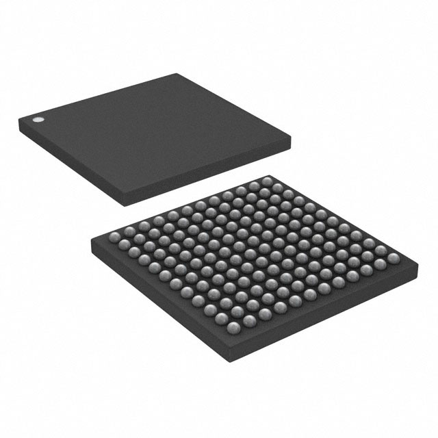


 工商网监
湘ICP备2023018690号
工商网监
湘ICP备2023018690号
