19-3671; Rev 0; 5/05
KIT
ATION
EVALU
LE
B
A
IL
A
AV
200mA Step-Up Converters in 6-Pin
SOT23 and TDFN
The MAX8569A/MAX8569B low-quiescent-current
boost regulators provide up to 200mA at output voltages up to 5.5V from a 1.5V to 5.5V input source. The
built-in synchronous rectifier allows for over 90% efficiency while achieving small size and low cost by eliminating the need for an external Schottky diode.
The MAX8569A provides an adjustable output while the
MAX8569B is fixed at 3.0V or 3.3V. The MAX8569B features a power-on reset output (RST) to signal that the
output has reached regulation. All devices connect the
battery input to the output during shutdown, allowing
the input battery to be used as a backup or real-time
clock supply when the converter is off.
Applications
Medical Diagnostic
Equipment
Cordless Phones
Digital Cameras
PC Cards
PDAs and Smartphones
Local 3.3V or 5V Supply
♦ 1.5V to 5.5V Input Voltage Range
♦ BATT Connected to OUT in Shutdown for Backup
Power
♦ Up to 95% Efficiency
♦ 7µA Typical Quiescent Current
♦ (0.5 x L x 0.780A2) / (r% x VOUT2)
where L is the inductor value and r is the desired output
ripple in %. A 22µF ceramic capacitor is a good starting value.
The input capacitor reduces the peak current drawn
from the battery and can be the same value as the output capacitor. A larger input capacitor can be used to
further reduce the input ripple and improve efficiency.
PC Board Layout and Grounding
Careful printed circuit layout is important for minimizing
ground bounce and noise. Keep the IC’s GND pin and
the ground leads of the input- and output-filter capacitors less than 0.2in (5mm) apart. In addition, keep all
connections to the FB and LX pins as short as possible.
In particular, when using external feedback resistors,
locate them as close to FB as possible. To maximize
output power and efficiency and minimize output ripple
voltage, use a ground plane and solder the IC’s GND
directly to the ground plane. A sample layout is available in the MAX8569A/MAX8569B evaluation kit to
speed designs.
Chip Information
PROCESS: BiCMOS
where VOUT is the desired output voltage and VFB is
1.228V.
Inductor Selection
The control scheme of the MAX8569A/MAX8569B permits flexibility in choosing an inductor. A 10µH inductor
performs well for most applications, but values from
4.7µH to 100µH can be used as well. Small inductance
values typically offer smaller physical size. Output
power is reduced when the inductance is large enough
to prevent the maximum current limit (780mA) from
being reached before the maximum on-time (5µs)
expires. For maximum output current, choose L so that:
VBATT(MAX) × 1µs
0.78A
IOUT(MAX) =
8
< L <
Selector Guide
OUTPUT
VOLTAGE
PINPACKAGE
TOP
MARK
Adjustable
SOT23-6
ABWK
MAX8569BEUT
Fixed 3.3V
SOT23-6
ABWL
MAX8569AETT
Adjustable
TDFN
AJN
MAX8569BETT
Fixed 3.3V
TDFN
AJO
MAX8569BETT30
Fixed 3.0V
TDFN
AJP
PART
MAX8569AEUT
VBATT(MIN) × 5µs
0.78A
0.78A
0.78A
× VBATT(MIN) −
× (RNCH + RL )
2
2
VOUT
_______________________________________________________________________________________
�200mA Step-Up Converters in 6-Pin
SOT23 and TDFN
6, 8, &10L, DFN THIN.EPS
D2
D
A2
PIN 1 ID
N
0.35x0.35
b
PIN 1
INDEX
AREA
E
[(N/2)-1] x e
REF.
E2
DETAIL A
e
k
A1
CL
CL
A
L
L
e
e
PACKAGE OUTLINE, 6,8,10 & 14L,
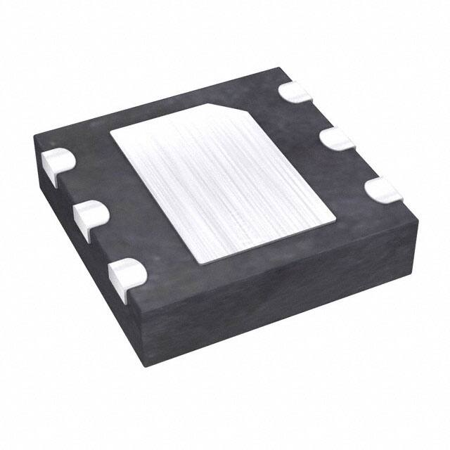
TDFN, EXPOSED PAD, 3x3x0.80 mm
-DRAWING NOT TO SCALE-
21-0137
G
1
2
_______________________________________________________________________________________
9
MAX8569A/MAX8569B
Package Information
(The package drawing(s) in this data sheet may not reflect the most current specifications. For the latest package outline information
go to www.maxim-ic.com/packages.)
�MAX8569A/MAX8569B
200mA Step-Up Converters in 6-Pin
SOT23 and TDFN
Package Information (continued)
(The package drawing(s) in this data sheet may not reflect the most current specifications. For the latest package outline information
go to www.maxim-ic.com/packages.)
COMMON DIMENSIONS
MIN.
MAX.
D
0.70
2.90
0.80
3.10
E
A1
2.90
0.00
3.10
0.05
L
k
0.20
0.40
0.25 MIN.
A2
0.20 REF.
SYMBOL
A
PACKAGE VARIATIONS
PKG. CODE
N
D2
E2
e
JEDEC SPEC
b
[(N/2)-1] x e
DOWNBONDS
ALLOWED
T633-1
6
1.50–0.10
2.30–0.10
0.95 BSC
MO229 / WEEA
0.40–0.05
1.90 REF
NO
T633-2
6
1.50–0.10
2.30–0.10
0.95 BSC
MO229 / WEEA
0.40–0.05
1.90 REF
NO
T833-1
8
1.50–0.10
2.30–0.10
0.65 BSC
MO229 / WEEC
0.30–0.05
1.95 REF
NO
T833-2
8
1.50–0.10
2.30–0.10
0.65 BSC
MO229 / WEEC
0.30–0.05
1.95 REF
NO
T833-3
8
1.50–0.10
2.30–0.10
0.65 BSC
MO229 / WEEC
0.30–0.05
1.95 REF
YES
T1033-1
10
1.50–0.10
2.30–0.10
0.50 BSC
MO229 / WEED-3
0.25–0.05
2.00 REF
NO
T1433-1
14
1.70–0.10
2.30–0.10
0.40 BSC
----
0.20–0.05
2.40 REF
YES
T1433-2
14
1.70–0.10
2.30–0.10
0.40 BSC
----
0.20–0.05
2.40 REF
NO
PACKAGE OUTLINE, 6,8,10 & 14L,
TDFN, EXPOSED PAD, 3x3x0.80 mm
-DRAWING NOT TO SCALE-
10
21-0137
______________________________________________________________________________________
G
2
2
�200mA Step-Up Converters in 6-Pin
SOT23 and TDFN
6LSOT.EPS
Maxim cannot assume responsibility for use of any circuitry other than circuitry entirely embodied in a Maxim product. No circuit patent licenses are
implied. Maxim reserves the right to change the circuitry and specifications without notice at any time.
Maxim Integrated Products, 120 San Gabriel Drive, Sunnyvale, CA 94086 408-737-7600 ____________________ 11
© 2005 Maxim Integrated Products
Printed USA
is a registered trademark of Maxim Integrated Products, Inc.
MAX8569A/MAX8569B
Package Information (continued)
(The package drawing(s) in this data sheet may not reflect the most current specifications. For the latest package outline information
go to www.maxim-ic.com/packages.)
�
很抱歉,暂时无法提供与“MAX8569BETT30+”相匹配的价格&库存,您可以联系我们找货
免费人工找货