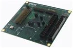
S1D13719 Mobile Graphics Engine
S5U13719P00C100
Evaluation Board User
Manual
SEIKO EPSON CORPORATION
Rev. 1.1
�Evaluation Board/Kit and Development Tool Important Notice
1.
This evaluation board/kit or development tool is designed for use for engineering evaluation, demonstration, or development purposes only. Do not use it for other purposes. It is not intended to meet the requirements of design for finished
products.
2.
This evaluation board/kit or development tool is intended for use by an electronics engineer and is not a consumer product.
The user should use it properly and in a safe manner. Seiko Epson does not assume any responsibility or liability of any
kind of damage and/or fire caused by the use of it. The user should cease to use it when any abnormal issue occurs even
during proper and safe use.
3.
The part used for this evaluation board/kit or development tool may be changed without any notice.
NOTICE
No part of this material may be reproduced or duplicated in any form or by any means without the written permission of Seiko
Epson. Seiko Epson reserves the right to make changes to this material without notice. Seiko Epson does not assume any liability of any kind arising out of any inaccuracies contained in this material or due to its application or use in any product or circuit and, further, there is no representation that this material is applicable to products requiring high level reliability, such as,
medical products. Moreover, no license to any intellectual property rights is granted by implication or otherwise, and there is
no representation or warranty that anything made in accordance with this material will be free from any patent or copyright
infringement of a third party. When exporting the products or technology described in this material, you should comply with
the applicable export control laws and regulations and follow the procedures required by such laws and regulations. You are
requested not to use, to resell, to export and/or to otherwise dispose of the products (and any technical information furnished,
if any) for the development and/or manufacture of weapon of mass destruction or for other military purposes.
All brands or product names mentioned herein are trademarks and/or registered trademarks of their respective companies.
©SEIKO EPSON CORPORATION 2007 - 2012, All rights reserved.
�Table of Contents
Chapter 1 Introduction . . . . . . . . . . . . . . . . . . . . . . . . . . . . . . . . . . . . 5
Chapter 2 Features . . . . . . . . . . . . . . . . . . . . . . . . . . . . . . . . . . . . . . 6
Chapter 3 Installation and Configuration . . . . . . . . . . . . . . . . . . . . . . . . . . 7
3.1 Configuration DIP Switch . . . . . . . . . . . . . . . . . . . . . . . . . . . 7
3.2 Configuration Jumpers . . . . . . . . . . . . . . . . . . . . . . . . . . . . 8
Chapter 4 Technical Description . . . . . . . . . . . . . . . . . . . . .
4.1 Power . . . . . . . . . . . . . . . . . . . . . . . . . .
4.1.1 Power Requirements . . . . . . . . . . . . . . . . . . . . . . . .
4.1.2 Voltage Regulators . . . . . . . . . . . . . . . . . . . . . . . . .
4.1.3 S1D13719 Power . . . . . . . . . . . . . . . . . . . . . . . . . .
4.2 Clocks . . . . . . . . . . . . . . . . . . . . . . . . . .
4.3 Reset . . . . . . . . . . . . . . . . . . . . . . . . . . .
4.4 Host Interface . . . . . . . . . . . . . . . . . . . . . . .
4.4.1 Direct Host Bus Interface Support . . . . . . . . . . . . . . . . .
4.4.2 Connecting to the Epson S5U13U00P00C100 USB Adapter Board
4.5 LCD Panel Interface . . . . . . . . . . . . . . . . . . . . .
4.6 Camera Interface . . . . . . . . . . . . . . . . . . . . . .
4.7 SD Card Interface . . . . . . . . . . . . . . . . . . . . . .
4.8 GPIO Connections . . . . . . . . . . . . . . . . . . . . .
Chapter 5 Parts List
.
.
.
.
.
.
.
.
.
.
.
.
.
.
. . . . . . .
. . . . . .
. . . . . . . .
. . . . . . . .
. . . . . . . .
. . . . . .
. . . . . .
. . . . . .
. . . . . . . .
. . . . . . . .
. . . . . .
. . . . . .
. . . . . .
. . . . . .
12
12
12
12
12
13
13
13
13
14
16
18
19
19
. . . . . . . . . . . . . . . . . . . . . . . . . . . . . . . . . . . . 20
Chapter 6 Schematic Diagrams . . . . . . . . . . . . . . . . . . . . . . . . . . . . . . 23
Chapter 7 S5U13719P00C100 Board Layout . . . . . . . . . . . . . . . . . . . . . . . 27
Chapter 8 References . . . . . . . . . . . . . . . . . . . . . . . . . . . . . . . . . . . 29
8.1 Documents . . . . . . . . . . . . . . . . . . . . . . . . . . . . . . . 29
8.2 Document Sources . . . . . . . . . . . . . . . . . . . . . . . . . . . . 29
Chapter 9 Change Record . . . . . . . . . . . . . . . . . . . . . . . . . . . . . . . . . 30
S5U13719P00C100 Evaluation Board User Manual (Rev. 1.1) EPSON
3
�4
EPSON
S5U13719P00C100 Evaluation Board User Manual (Rev. 1.1)
�Chapter 1 Introduction
Chapter 1 Introduction
This manual describes the setup and operation of the S5U13719P00C100 Evaluation Board. The evaluation board
is designed as an evaluation platform for the S1D13719 Mobile Graphics Engine.
The S5U13719P00C100 evaluation board can connect to the S5U13U00P00C100 USB Adapter board so that it can
be used with a laptop or desktop computer, via USB 2.0. The S5U13719P00C100 evaluation board can also be used
with many other native platforms via the host connectors which provide the appropriate signals to support a variety
of CPUs.
This user manual is updated as appropriate. Please check the Epson Research and Development Website at
www.erd.epson.com for the latest revision of this document before beginning any development.
We appreciate your comments on our documentation. Please contact us via email at documentation@erd.epson.com.
S5U13719P00C100 Evaluation Board User Manual (Rev. 1.1) EPSON
5
�Chapter 2 Features
Chapter 2 Features
The S5U13719P00C100 Evaluation Board includes the following features:
• 180-pin PFBGA S1D13719 Mobile Graphics Engine
• Headers for connection to the S5U13U00P00C100 USB Adapter board
• Headers for connecting to various Host Bus Interfaces
• Headers for connecting to LCD panels
• Headers for connecting to cameras
• On-board 32.768kHz oscillator
• 14-pin DIP socket (if an oscillator other than 32.768kHz must be used)
• SD Card interface (optional)
• 3.3V input power
• On-board voltage regulators for 1.8V and for 2.7V
• On-board voltage regulator with adjustable 12~25V output, 60~100mA max., to provide power for LED backlight of LCD panels.
6
EPSON
S5U13719P00C100 Evaluation Board User Manual (Rev. 1.1)
�Chapter 3 Installation and Configuration
Chapter 3 Installation and Configuration
The S5U13719P00C100 evaluation board incorporates a DIP switch, jumpers, and 0 ohm resistors which allow it to
be used with a variety of different configurations.
3.1 Configuration DIP Switch
The S1D13719 has configuration inputs (CNF[7:0]) which are read on the rising edge of RESET#. An 8-position
DIP switch (SW1) is used to configure the S1D13719 for multiple Host Bus Interfaces. The following figure shows
the location of DIP switch SW1 on the S5U13719P00C100.
SW1
Figure 3-1: Configuration DIP Switch (SW1) Location
S5U13719P00C100 Evaluation Board User Manual (Rev. 1.1) EPSON
7
�Chapter 3 Installation and Configuration
All S1D13719 configuration inputs (CNF[7:0]) are fully configurable using DIP switch SW1 as described below.
Power-On/Reset State
S5U13719P00C100
SW1-[8:1] Config
S1D13719
CNF[7:0] Config
SW1-[8]
CNF7
Camera2 power supply OFF
Camera2 power supply ON
SW1-[7]
CNF6
Parallel 2 CS# mode
Parallel 1 CS# mode
SW1-[6]
CNF5
Big endian
Little Endian
SW1-[5:3]
CNF[4:2]
SW1-[2]
CNF5
SW1-[1]
CNF6
1 (ON)
0 (OFF)
000b
Direct 80 Type 2 host interface
001b
Direct 80 Type 3 host interface
010b
Indirect 80 Type 2 host interface
011b
Indirect 80 Type 3 host interface
100b
Direct 80 Type 1 host interface
101b
Direct 68 host interface
110b
Indirect 80 Type 1 host interface
111b
Indirect 68 host interface
GPIO[21:0] configured as inputs
Camera1 power supply ON
GPIO[21:0] configured as outputs
Camera1 power supply ON
= Required settings when using S5U13U00P00C100 USB Adapter board (SW1-[8:1] = 000000x0b)
3.2 Configuration Jumpers
The S5U13719P00C100 has 9 jumpers which configure various board settings. The jumper positions for each
function are shown below.
Jumper
Function
Position 1-2
Position 2-3
JP1
COREVDD
Normal
—
JP2
PLLVDD
Normal
—
JP3
HIOVDD
Normal
—
JP4
PIOVDD
Normal
—
JP5
JP6
HIOVDD Source
PIOVDD Source
H1 connector, pin 32
H4 connector, pin 8
3.3VDD
3.3VDD
JP7
CIO1VDD
Normal
—
JP8
CIO2VDD
Normal
—
JP9
SIOVDD
Normal
—
No Jumper
COREVDD current
measurement
PLLVDD current
measurement
HIOVDD current
measurement
PIOVDD current
measurement
—
—
CIO1VDD current
measurement
CIO2VDD current
measurement
SIOVDD current
measurement
= Required settings when using S5U13U00P00C100 USB Adapter board
8
EPSON
S5U13719P00C100 Evaluation Board User Manual (Rev. 1.1)
�Chapter 3 Installation and Configuration
JP1-JP4 and JP7-JP9 - Power Supplies for S1D13719
JP1-JP4 and JP7-JP9 can be used to measure current consumption of each S1D13719 power supply.
When the jumper is at position 1-2, normal operation is selected.
When no jumper is installed, the current consumption for each power supply can be measured by connecting an
ammeter to pin 1 and 2 of the jumper.
The jumper associated to each power supply is as follows:
JP1 for COREVDD
JP2 for PLLVDD
JP3 for HIOVDD
JP4 for PIOVDD
JP7 for CIO1VDD
JP8 for CIO2VDD
JP9 for SIOVDD
JP8
JP7
JP1
JP2
JP3
JP4
JP9
Figure 3-2: Configuration Jumper Locations (JP1-JP4 and JP7-JP9)
S5U13719P00C100 Evaluation Board User Manual (Rev. 1.1) EPSON
9
�Chapter 3 Installation and Configuration
JP5 - HIOVDD Source
JP5 is used to select the source for the HIOVDD supply voltage.
When the jumper is at position 1-2, the HIOVDD voltage must be provided to the H1 connector, pin 32.
When the jumper is at position 2-3, the HIOVDD voltage is provided by the 3.3V power supply of the board.
JP5
Figure 3-3: Configuration Jumper Location (JP5)
10
EPSON
S5U13719P00C100 Evaluation Board User Manual (Rev. 1.1)
�Chapter 3 Installation and Configuration
JP6 - PIOVDD Source
JP6 is used to select the source for the PIOVDD supply voltage.
When the jumper is at position 1-2, the PIOVDD voltage must be provided to the H6 connector, pin 1.
When the jumper is at position 2-3, the PIOVDD voltage is provided by the 3.3V power supply of the board.
JP6
Figure 3-4: Configuration Jumper Location (JP6)
S5U13719P00C100 Evaluation Board User Manual (Rev. 1.1) EPSON
11
�Chapter 4 Technical Description
Chapter 4 Technical Description
4.1 Power
4.1.1 Power Requirements
The S5U13719P00C100 evaluation board requires an external regulated power supply (3.3V at 1A). The power is
supplied to the evaluation board through pin 5 of the P2 header, or pin 29 of the H1 header.
The green LED ‘3.3V Power’ is turned on when 3.3V power is applied to the board.
4.1.2 Voltage Regulators
The S5U13719P00C100 evaluation board has on-board linear regulators to provide the different voltage required by
the S1D13719 Mobile Graphics Engine. It also has a step-up switching voltage regulator to generate adjustable
12~25V, which can be used to power the LED backlight on some LCD panels.
4.1.3 S1D13719 Power
The S1D13719 Mobile Graphics Engine requires 1.8V and 2.5V or 3.0V power supplies.
COREVDD and PLLVDD use 1.8V power, which is provided by an on-board linear voltage regulator.
HIOVDD power can be selected with jumper JP5. When JP5 is set to the 2-3 position, HIOVDD is connected to
3.3V. If a different voltage is required for HIOVDD, set JP5 to the 1-2 position and connect the external power
supply to pin 32 of connector H1.
PIOVDD power can be selected with jumper JP6. When JP6 is set to the 2-3 position, PIOVDD is connected to 3.3V.
If a different voltage is needed for PIOVDD because of the LCD panel requirements, set JP6 to the 1-2 position and
connect the external power supply to pin 1 of connector H6.
CIO1VDD is connected to 2.7V, which is provided by an on-board linear regulator, through a 0 ohm resistor, R9. If
it is desired to have a different voltage for CIO1VDD, R9 must be removed and the desired supply connected to pin
15 of connector H3.
CIO2VDD is connected to 2.7V, which is provided by an on-board linear regulator, through a 0 ohm resistor, R10.
If it is desired to have a different voltage for CIO1VDD, R10 must be removed and the desired supply connected to
pin 15 of connector H7.
SIOVDD is connected to PIOVDD through a 0 ohm resistor, R11. If it is desired to have a different voltage for
SIOVDD, R11 must be removed and the desired supply connected to pin 4 of connector J1.
12
EPSON
S5U13719P00C100 Evaluation Board User Manual (Rev. 1.1)
�Chapter 4 Technical Description
4.2 Clocks
The clock for the S1D13719 Mobile Graphics Engine is provided by a 32.768kHz oscillator.
The S5U13719P00C100 evaluation board has a DIP14 footprint for an optional second oscillator, Y2. This is
provided for cases requiring a different clock frequency for the S1D13719 Mobile Graphics Engine. To use Y2, an
oscillator must be populated in the Y2 footprint and the following board modifications must be made.
1. Remove R20 (33 ohm resistor, size 0402) to cut the output of Y1.
2. Populate R23 with a 33 ohm resistor, size 0402, to connect the output of Y2 to the CLKI input of the
S1D13719 Mobile Graphics Engine.
4.3 Reset
The S5U13719P00C100 evaluation board can be reset using a push-button, or via an active low reset signal from
the host development platform, on pin 30 of connector H1.
The reset signal will reset the S1D13719 Mobile Graphics Engine and is also available on the H3 and H7 connectors,
so that camera modules connected to the board can be reset.
4.4 Host Interface
4.4.1 Direct Host Bus Interface Support
All S1D13719 host interface pins are available on connector H1 and H2 which allows the S5U13719P00C100 evaluation board to be connected to a variety of development platforms. For detailed S1D13719 pin mapping, refer to the
S1D13719 Hardware Functional Specification, document number X59A-A-001-xx.
The following figure shows the location of host bus connector H1 and H2. H1 and H2 are 0.1x0.1”, 34-pin headers
(17x2).
S5U13719P00C100 Evaluation Board User Manual (Rev. 1.1) EPSON
13
�Chapter 4 Technical Description
H1
H2
Figure 4-1: Host Bus Connector Location (H1 and H2)
For the pinout of connectors H1 and H2, see Section Chapter 6, “Schematic Diagrams” on page 23.
4.4.2 Connecting to the Epson S5U13U00P00C100 USB Adapter Board
The S5U13719P00C100 evaluation board is designed to connect to the S5U13U00P00C100 USB Adapter Board.
The USB adapter board provides a simple connection to any computer via a USB 2.0 connection. The
S5U13719P00C100 directly connects to the USB adapter board through connectors P1 and P2.
The USB adapter board also supplies the 3.3V power required by the S5U13719P00C100. HIOVDD should be
selected for 3.3V and JP5 should be set to the 2-3 position.
When the S5U13719P00C100 is connected to the S5U13U00P00C100 USB Adapter board, there are 2 LEDs on
S5U13719P00C100 which provide a quick visual status of the USB adapter. LED1 blinks to indicate that the USB
adapter board is active. LED2 turns on to indicate that the USB has been enumerated by the PC.
The following diagram shows the location of connectors P1 and P2. P1 and P2 are 2mm x 2mm, 40-pin headers
(20x2).
14
EPSON
S5U13719P00C100 Evaluation Board User Manual (Rev. 1.1)
�Chapter 4 Technical Description
P2
P1
Figure 4-2: USB Adapter Connector Locations (P1 and P2 - Board Bottom)
For the pinout of connectors P1 and P2, see Section Chapter 6, “Schematic Diagrams” on page 23.
Note
A windows driver must be installed on the PC when the S5U13719P00C100 is used with the S5U13U00P00C100
USB Adapter Board. The S1D13xxxUSB driver is available at www.erd.epson.com.
S5U13719P00C100 Evaluation Board User Manual (Rev. 1.1) EPSON
15
�Chapter 4 Technical Description
4.5 LCD Panel Interface
The LCD interface signals are available on connectors H4 and H5. For S1D13719 LCD interface pin mapping, refer
to the S1D13719 Hardware Functional Specification, document number X59A-A-001-xx.
On the evaluation board there is an adjustable 12~25V power supply. At 12V, the maximum current available is
100mA. At 25V, the maximum current available is 60mA. This power supply is intended to use to power the LED
backlight on some LCD panels. The voltage is adjusted by the R36 pot.
Note
For LCD panels that use CCFL backlight, an external power supply must be used to provide power to the inverter
for CCFL backlight. Usually, the inverter current consumption is higher than the maximum 100mA current available from the on-board voltage regulator.
The following diagram shows the location of the LCD panel connectors H4 and H5. H4 and H5 are both 0.1x0.1”,
40-pin headers (20x2).
16
EPSON
S5U13719P00C100 Evaluation Board User Manual (Rev. 1.1)
�Chapter 4 Technical Description
H5
H4
Figure 4-3: LCD Panel Connectors Locations (H4, H5)
For the pinout of connectors H4 and H5, see Section Chapter 6, “Schematic Diagrams” on page 23.
S5U13719P00C100 Evaluation Board User Manual (Rev. 1.1) EPSON
17
�Chapter 4 Technical Description
4.6 Camera Interface
All the signals for the Camera1 interface are available on connector H3. All the signals for the Camera2 interface
are available on connector H7.
Camera modules are programmed using an I2C type bus. The S1D13719 does not have an I2C interface, but it has
GPIOs that can be used to emulate the I2C bus. By default, the board uses GPIO17 as SCL signal of I2C bus and
GPIO18 as SDA signal of I2C bus. If GPIO17 and GPIO18 must be used for some other function, for example SD
Card interface, than GPIO1 can be selected for SCL by removing R38 and populating R37 with a 0Ω resistor, size
0402. GPIO2 can be selected for SDA by removing R44 and populating R43 with a 0Ω resistor, size 0402.
The I2C bus lines must be pulled high. The default configuration of the evaluation board has the I2C lines, SCL and
SDA, pulled high to CIO1VDD. If the I2C lines must be pulled high to CIO2VDD, R34 and R41 must be removed
and 2.2kΩ resistors, size 0402, must be mounted for R35 and R42.
The reset signal provided on H3 and H7 is active low and is pulled to HIOVDD when inactive.
The S1D13719 camera interface has a strobe output, CMSTROUT, that is available on H6 connector. Note that
connector H6 is not populated on the S5U13719P00C100 evaluation board.
The following diagram shows the location of the camera connectors H3, H6 and H7. H3 and H7 are 0.1x0.1”, 20pin headers (10x2). H6 is 0.1”, 6-pin header (6x1).
H6
H7
H3
Figure 4-4: Camera Expansion Connector Locations (H3, H6 and H7)
For the pinout of connectors H3, H6 and H7, see Section Chapter 6, “Schematic Diagrams” on page 23.
18
EPSON
S5U13719P00C100 Evaluation Board User Manual (Rev. 1.1)
�Chapter 4 Technical Description
4.7 SD Card Interface
The S1D13719 Mobile Graphics Engine has a SD Card interface. The S5U13719P00C100 evaluation board is
designed with a SD Card socket, J1. Note that J1 socket and related components, R13-R19 and C37-39, are not
populated on the S5U13719P00C100 evaluation board.
The SD Card interface has a general purpose output pin GPIO19/SDGPO, which is used to turn on a LED (D1). Note
that D1 LED and related components, U2, C42 and R21, are not populated on the S5U13719P00C100 evaluation
board.
The following figure shows the location of the SD Card connector (J1) and the SD Card LED (D1).
D1
J1
Figure 4-5: SD Card J1 Connector Location
4.8 GPIO Connections
The S1D13719 Mobile Graphics Engine has 22 GPIO pins. Some GPIOs have multiple functions. The GPIO pins
are routed to the connectors on the S5U13719P00C100 evaluation board. If any pin is configured as a GPIO, it will
be available on the connectors as listed below:
• GPIO[10:0] pins are routed to connector H5.
• GPIO[18:11] pins are routed to connector J1. Note that connector J1 is not populated on the S5U13719P00C100
evaluation board.
• GPIO[19] pin is not routed to any connector on the board. It is routed only to pin 2 of U2 footprint on the board.
Note that U2 is not populated on the S5U13719P00C100 evaluation board.
• GPIO[21:20] pins are routed to connector H6. Note that connector H6 is not populated on the
S5U13719P00C100 evaluation board.
S5U13719P00C100 Evaluation Board User Manual (Rev. 1.1) EPSON
19
�Chapter 5 Parts List
Chapter 5 Parts List
Table 5-1: Parts List
Item Qty
Reference
Part
Description
Manufacturer Part No
24
C1,C2,C3,C4,C5,C6,
C13,C16,C17,C18,
C19,C20,C21,C22,
C30,C31,C32,C36,
C40,C43,C45,C47,
C50,C52
0.1uF
C0402
Yageo America
04022F104Z7B20D
2
18
C7,C8,C9,C10,C11,
C12,C23,C24,C25,
C26,C27,C28,C29,
C33,C34,C35,C41,
C44
0.01uF
CAP 10000PF 16V CERAMIC
X7R 0402 C0402
Kemet
C0402C103K4RACTU
3
1
C14
1nF
C0402
Yageo America
04022R102K9B20D
4
1
C15
10uF
C0805
Panasonic - ECG
ECJ-CV50J106M
5
0
C37
NP_10uF
C0805
Panasonic - ECG
ECJ-2FB1A106K
6
0
C38,C42
NP_0.1uF
C0402
Yageo America
04022F104Z7B20D
7
0
C39
NP_0.01uF
C0402
Kemet
C0402C103K4RACTU
8
2
C46,C48
4.7uF 10V T
CAPACITOR TANT 4.7UF
10V 10% SMD C3528
Kemet
T494B475K010AT
9
2
C49,C51
1uF
C0402
Panasonic - ECG
ECJ-0EB0J105M
10
1
C53
2.2uF 10V
CAP CER 2.2UF 10V X7R
0805 C0805
Taiyo Yuden
LMK212BJ225KG-T
11
1
C54
10uF 35V
CAP CER 10UF 35V X5R
1210 C1206
Taiyo Yuden
GMK325BJ106KN-T
12
1
C55
150pF
C0402
Panasonic - ECG
ECJ-0EC1H151J
13
0
D1
NP_SD Card
LED GREEN SS TYPE LOW
CUR SMD LED0603
Panasonic - SSG
LNJ308G8LRA
14
3
D2,D3,D4
LED GREEN SS TYPE LOW
CUR SMD LED0603
Panasonic - SSG
LNJ308G8LRA
15
1
D5
MBR0540
SOD-123
Micro Commercial Co.
MBR0540-TP
16
1
F1
ACH32C-333-T
FILTR 3TERM 10MHZ TO
300MHZ SMD
TDK
ACH32C-333-T
17
1
F2
ACF451832-222
FILTER 3-TERM 60MHZ
300MA SMD
TDK
ACF451832-222
18
2
H1,H2
HEADER_17X2
Samtec
TSW-117-07-G-D
19
2
H3,H7
HEADER_10X2
Samtec
TSW-110-07-G-D
1
20
EPSON
S5U13719P00C100 Evaluation Board User Manual (Rev. 1.1)
�Chapter 5 Parts List
Table 5-1: Parts List
Item Qty
Reference
Part
Description
Manufacturer Part No
LCD Connector
Samtec
TST-120-01-G-D
Samtec
TST-120-01-G-D
20
1
H4
HEADER_20X2
Shrouded
21
1
H5
HEADER_20X2
Shrouded
Extended LCD Connector
22
0
H6
AUX
CONN HEADER VERT 6POS
.100 TIN or GENERIC
23
7
JP1,JP2,JP3,JP4,
JP7,JP8,JP9
CONN HEADER VERT 2POS
.100 TIN or GENERIC SIP2
24
2
JP5,JP6
CONN HEADER VERT 3POS
.100 TIN or GENERIC SIP3
25
0
J1
NP_DMM1AA-SFPEJ
26
2
L1,L2
Ferrite
FERRITE 200MA 938 OHMS
0603 SMD R0603
Steward
HZ0603B751R-10
27
1
L3
10uH
COIL 10UH 1300MA CHOKE
SMD IND_ELL6
Panasonic - ECG
ELL-6SH100M
28
2
P1,P2
HEADER_20X2
HDR2X20/2MM
3M
151240-8422-RB
29
9
R1,R2,R3,R4,R5,R6,
R7,R8,R33
10k
R0402
30
6
R9,R10,R11,R26,R2
7,R31
0
R0603
31
1
R12
150k 1%
R0402
32
0
R13,R14,R15,R16,
R17,R18,R19
NP_47k
R0402
33
1
R20
33 1%
R0402
34
0
R21
NP_180
R0402
35
0
R22,R23,R35,R37,
R42,R43
NP
R0402
36
4
R24,R25,R38,R44
0
R0402
37
3
R28,R29,R30
270 1%
R0402
38
1
R32
120k
R0402
39
1
R39
56k
R0402
40
2
R34,R41
2.2k
R0402
41
1
R36
200k
POT 200K OHM 3MM
CARBON TRIM SMD
42
1
R40
13.3k 1%
R0402
43
9
SH1,SH2,SH3,SH4,
SH5,SH6,SH7,SH8,
SH9
.100 in. Jumper
Shunt
JUMPER SHORTING TIN
44
1
SW1
SW8_DIPSW8
DIPSW8
ITT Industries
KSC241GLFS
Keystone
5015
Hirose
DM1AA-SF-PEJ
45
1
SW2
SW TACT-SPST
SWITCH TACT SILVER PLT
GULLWING SW_EVQQW
46
2
TPGND1,
TP3.3VDD1
TP_SMT
PC TEST POINT MINIATURE
SMT TP_1206
S5U13719P00C100 Evaluation Board User Manual (Rev. 1.1) EPSON
Panasonic - ECG
EVN-5ESX50B25
Sullins Electronics Corp.
STC02SYAN
21
�Chapter 5 Parts List
Table 5-1: Parts List
Item Qty
Reference
Part
47
1
U1
S1D13719PFBGA
Description
Manufacturer Part No
48
0
U2
NP_74LVC1G126
IC BUS BUFFER GATE 3-ST
SOT-23-5
Texas Instruments
SN74LVC1G126DBVR
49
1
U3
TPS76918DBVR
IC 1.8V 100MA LDO REG
SOT-23-5
Texas Instruments
TPS76918DBVR
50
1
U4
TPS76927DBVT
IC 2.7V 100MA LDO REG
SOT-23-5
Texas Instruments
TPS76927DBVT
51
1
U5
LM2733Y
IC CONV BOOST 40V FET
SW SOT23-5
National Semiconductor
LM2733YMF/NOPB
52
1
Y1
32.768kHz OSC
OSC 32.768KHZ 523PPM
SMD
Epson
SG-3030JC 32.7680KB3:ROHS
53
0
Y2
14-Pin DIP
22
AMP
2-641609-1
EPSON
S5U13719P00C100 Evaluation Board User Manual (Rev. 1.1)
�A
B
C
SW1
8
7
6
5
4
3
2
1
SW8_DIPSW8
9
10
11
12
13
14
15
16
PIOVDD
10k
R1
5
10k
R2
10k
R3
10k
R4
10k
R5
10k
R6
3
3
10k
R7
10k
R8
DB[15:0]
AB[18:1]
GPIO21
GPIO20
GPIO19/SDGPO
GPIO18/SDWP
GPIO17/SDCD#
GPIO16/SDCLK
GPIO15/SDCMD
GPIO14/SDDAT3
GPIO13/SDDAT2
GPIO12/SDDAT1
GPIO11/SDDAT0
GPIO10
GPIO9
GPIO8
GPIO7
GPIO6
GPIO5
GPIO4
GPIO3
GPIO2
GPIO1
GPIO0
SCS#
SCK
SA0
SI
3
3
3
3
4
4
2
2,4
2,4
2
2
2
2
2
2
4
4
4
4
4
4
4
4
4
4
4
CLKI
INT
CS#
M/R#
RD#
WE#
BE1#
BE0#
WAIT#
RESET#
2
3
3
3
3
3
3
3
3
2,3,4
E4
D2
E3
A8
C8
B9
A9
B2
D4
A2
E5
B4
C4
A3
F5
D5
DB0
DB1
DB2
DB3
DB4
DB5
DB6
DB7
DB8
DB9
DB10
DB11
DB12
DB13
DB14
DB15
N11
P11
F1
F2
G3
G2
G1
H3
H2
H1
G4
N10
P10
N12
P12
M11
M12
M13
P13
N13
L10
L1
J10
H5
K5
L5
J5
L9
K9
K6
A10
D10
E2
F3
A12
D1
B13
B12
B10
C10
A11
B11
C9
E1
A4
B5
C5
E6
A5
B6
C6
B7
D7
E7
A7
B8
C7
D8
C2
C3
C1
D3
AB1
AB2
AB3
AB4
AB5
AB6
AB7
AB8
AB9
AB10
AB11
AB12
AB13
AB14
AB15
AB16
AB17
AB18
4
GPIO21
GPIO20
GPIO19/SDGPO
GPIO18/SDWP
GPIO17/SDCD#
GPIO16/SDCLK
GPIO15/SDCMD
GPIO14/SDDAT3
GPIO13/SDDAT2
GPIO12/SDDAT1
GPIO11/SDDAT0
GPIO10
GPIO9
GPIO8
GPIO7
GPIO6
GPIO5
GPIO4
GPIO3
GPIO2
GPIO1
GPIO0
CNF7
CNF6
CNF5
CNF4
CNF3
CNF2
CNF1
CNF0
SCS#
SCLK
SA0
SI
CLKI
INT
CS#
M/R#
RD#
WE#
BE1#
BE0#
WAIT#
RESET#
DB0
DB1
DB2
DB3
DB4
DB5
DB6
DB7
DB8
DB9
DB10
DB11
DB12
DB13
DB14
DB15
AB1
AB2
AB3
AB4
AB5
AB6
AB7
AB8
AB9
AB10
AB11
AB12
AB13
AB14
AB15
AB16
AB17
AB18
U1
CORE
PLL
E11
PLLVDD
HIO
PIO
CIO2
CIO1
SIO
P6
M10
J3
H4
PIOVDD
PIOVDD
PIOVDD
PIOVDD
F4
D9
A6
HIOVDD
HIOVDD
HIOVDD
G5
FPCS1#
FPCS2#
FPSCLK
FPA0
FPSO
FPVIN1
FPVIN2
FPDAT0
FPDAT1
FPDAT2
FPDAT3
FPDAT4
FPDAT5
FPDAT6
FPDAT7
FPDAT8
FPDAT9
FPDAT10
FPDAT11
FPDAT12
FPDAT13
FPDAT14
FPDAT15
FPDAT16
FPDAT17
FPFRAME
FPLINE
FPSHIFT
DRDY
S1D13719PFBGA
NC
NC
NC
NC
NC
NC
NC
NC
NC
NC
NC
NC
NC
NC
VCP
SCANEN
TESTEN
OSCKO
OSCKI
OSCKMI
OSCMO
CM2DAT0
CM2DAT1
CM2DAT2
CM2DAT3
CM2DAT4
CM2DAT5
CM2DAT6
CM2DAT7
CM2VREF
CM2HREF
CM2CLKOUT
CM2CLKIN
CMSTROUT
CM1DAT0
CM1DAT1
CM1DAT2
CM1DAT3
CM1DAT4
CM1DAT5
CM1DAT6
CM1DAT7
CM1VREF
CM1HREF
CM1CLKOUT
CM1CLKIN
SIOVDD
4
CIO1VDD
CIO2VDD
J11
G11
VSS
VSS
VSS
VSS
VSS
VSS
VSS
VSS
VSS
K8
H13
E9
E8
D6
D11
COREVDD
COREVDD
COREVDD
COREVDD
COREVDD
COREVDD
PLLVSS
C12
S5U13719P00C100 Evaluation Board User Manual (Rev. 1.1) EPSON
E10
P9
M5
L11
K2
J2
H10
B1
B14
D
5
P1
P14
N9
N7
N4
J14
J1
G10
F12
C11
B3
A14
A13
A1
D12
L4
K1
C14
C13
D13
D14
E13
E12
F10
E14
F11
G12
F13
F14
G13
H12
G14
H14
N14
K11
K12
K13
L14
K10
L12
M14
L13
J12
H11
J13
K14
N5
M2
K7
P7
M9
J4
K3
L3
N1
K4
P2
N2
N3
M3
L6
L2
M6
M8
L8
P8
N8
M7
M4
L7
N6
P3
P4
P5
M1
CM2DAT0
CM2DAT1
CM2DAT2
CM2DAT3
CM2DAT4
CM2DAT5
CM2DAT6
CM2DAT7
CM2VREF
CM2HREF
CM2CLKOUT
CM2CLKIN
CMSTROUT
CM1DAT0
CM1DAT1
CM1DAT2
CM1DAT3
CM1DAT4
CM1DAT5
CM1DAT6
CM1DAT7
CM1VREF
CM1HREF
CM1CLKOUT
CM1CLKIN
FPCS1#
FPCS2#
FPSCK
FPA0
FPSO
FPVIN1
FPVIN2
FPFRAME
FPLINE
FPSHIFT
DRDY
FPDAT0
FPDAT1
FPDAT2
FPDAT3
FPDAT4
FPDAT5
FPDAT6
FPDAT7
FPDAT8
FPDAT9
FPDAT10
FPDAT11
FPDAT12
FPDAT13
FPDAT14
FPDAT15
FPDAT16
FPDAT17
4
4
4
4
4
4
4
4
4
4
4
4
4
4
4
4
4
4
4
4
4
4
4
4
4
4
4
4
4
4
4
4
4
4
4
4
3
FPDAT[17:0]
3
4
0.1uF
C24
0.01uF
C23
0.01uF
0.01uF
0.01uF
C10
0.1uF
C4
0.01uF
C25
0.1uF
C18
.100
SH6
0.1uF
2
Place a 0.01uF and a 0.1uF cap on each
CIO1VDD power pin of the S1D13719
0.01uF
0.01uF
C12
0.1uF
C6
3.3VDD
PIOVDD
PIOVDD_IN
Date:
Size
C
Title
0.01uF
C27
0.1uF
C20
PIO
0.01uF
C28
0.1uF
C21
0.01uF
C29
0.1uF
C22
1
0.01uF
C35
0.1uF
C32
R11
0
SIOVDD
SIO
Sheet
1
of
4
Rev
1.0
Place a 0.01uF and a 0.1uF cap on each
SIOVDD power pin of the S1D13719
SIOVDD
2
1
.100 in. Jumper Shunt
SH9
JP9
PIOVDD
Place a 0.01uF and a 0.1uF cap on each
PIOVDD power pin of the S1D13719
0.01uF
C26
0.1uF
C19
PIOVDD
1
Wednesday, October 17, 2007
Document Number
S1D13719 PFBGA-180
PIOVDD
2
1
.100 in. Jumper Shunt
SH4
JP4
C15
10uF
Place a 0.01uF and a 0.1uF cap on each
CIO2VDD power pin of the S1D13719
0.01uF
C34
C31
R10
0
CIO2VDD
CIO2
2.7VDD
0.1uF
C33
0.01uF
C11
0.1uF
C5
PIOVDD SOURCE
3
2
1
JP6
in. Jumper Shunt
C30
CIO2VDD
.100 in. Jumper Shunt
SH8
JP8
CIO1VDD
C14
1nF
PLL
L1
Ferrite
L2
Ferrite
0.1uF
C13
Place a 0.01uF and a 0.1uF cap on each
HIOVDD power pin of the S1D13719
C17
0.1uF
HIO
C16
HIOVDD
PLLVDD
2
1
.100 in. Jumper Shunt
1.8VDD
SH2
JP2
2
1
R9
0
CIO1VDD
CIO1
2.7VDD
3.3VDD
HIOVDD
HIOVDD_IN
2
1
HIOVDD
JP3
in. Jumper Shunt
0.01uF
0.01uF
C9
0.1uF
C3
Place a 0.01uF and a 0.1uF cap on each COREVDD
and OSCVDD power pin of the S1D13719
C8
0.1uF
C7
C2
0.1uF
CORE
C1
COREVDD
2
1
.100 in. Jumper Shunt
SH1
1.8VDD
JP1
2
1
.100 in. Jumper Shunt
SH7
JP7
HIOVDD SOURCE
3
2
1
.100 in. Jumper Shunt
SH5
JP5
.100
SH3
2
A
B
C
D
Chapter 6 Schematic Diagrams
Chapter 6 Schematic Diagrams
Figure 6-1: S5U13719P00C100 Schematics (1 of 4)
23
�A
B
C
1
1
1
1,4
1,4
5
GPIO11/SDDAT0
GPIO12/SDDAT1
GPIO13/SDDAT2
GPIO18/SDWP
GPIO17/SDCD#
1 GPIO16/SDCLK
1 GPIO14/SDDAT3
1 GPIO15/SDCMD
C42
NP_47k
R14
1 GPIO19/SDGPO
NP_0.1uF
NP_47k
R13
2
SIOVDD
NP_47k
R15
1
D
TP1
5
3
R21
4
SIOVDD
D1
NP_SD Card
C37
SIOVDD
NP_10uF
NP_DMM1AA-SF-PEJ
NP_47k
J1
1
SDDAT3
2
SDCMD
3
GND
4
VDD
5
SDCLK
6
GND
7
SDDAT0
8
SDDAT1
9
SDDAT2
10
SDWP
11
CDIN
12
GND
R19
SIOVDD
NP_47k
R18
NP_180
NP_47k
R17
U2
NP_74LVC1G126
4
NP_47k
R16
4
3
NP_0.1uF
C38
3
NP_0.01uF
C39
0.01uF
0.1uF
0.1uF
C47
3.3VDD
0.1uF
C45
R25
R24
0.01uF
0.1uF
3.3VDD
C44
C43
HIOVDD
C41
C40
HIOVDD
3
1
0
0
2
7
14
2
4
OUT
VIO
R22
2
3
1
2
3
1
NC/FB
Vout
8
1
NC/FB
Vout
Date:
Size
B
Title
TPS76927DBVT
GND
/EN
Vin
U4
TPS76918DBVR
GND
/EN
Vin
U3
TTL/CMOS
Oscillator
OE
NP
OUT
14-Pin DIP
GND
VDD
Y2
3
1
0.1uF
C36
R12
150k 1%
HIOVDD
32.768kHz OSC
GND
VDD
Y1
SW TACT-SPST
4
2
SW2
2
4
5
4
5
+
TP4
+
TP3
C46
1.8VDD
TP2
2.7VDD
4.7uF 10V T
C48
4.7uF 10V T
NP
33 1%
1,3,4
CLKI
Wednesday, October 17, 2007
Document Number
SD Card / Clocks / Reset / 1.8V Supply
R23
R20
RESET#
1
2
EPSON
1
24
2
5
1
Sheet
1
1
2
of
4
Rev
1.0
A
B
C
D
Chapter 6 Schematic Diagrams
Figure 6-2: S5U13719P00C100 Schematics (2 of 4)
S5U13719P00C100 Evaluation Board User Manual (Rev. 1.1)
�A
B
C
5
R107
R108
3.3VDD
TP3.3VDD1
TP_SMT
HIOVDD
0
0
CS#
R28
270 1%
HEARTBEAT
AB6
AB4
AB2
AB15
AB13
AB11
AB9
AB17
HEARTBEAT
DB6
DB4
DB2
DB0
DB15
DB13
DB11
DB9
RD#
INT
BE1#
4
4
D2
LED1
2
4
6
8
10
12
14
16
18
20
22
24
26
28
30
32
34
36
38
40
HEADER_20X2
P2
HEADER_20X2
2
4
6
8
10
12
14
16
18
20
22
24
26
28
30
32
34
36
38
40
R29
270 1%
ENUMERATED
1
3
5
7
9
11
13
15
17
19
21
23
25
27
29
31
33
35
37
39
1
3
5
7
9
11
13
15
17
19
21
23
25
27
29
31
33
35
37
39
P1
A
K
A
K
D3
LED2
AB16
AB14
AB12
AB10
AB8
AB7
AB5
AB3
AB1
AB18
R197
270 1%
3.3VDD
ENUMERATED
M/R#
DB14
DB12
DB10
DB8
DB7
DB5
DB3
DB1
WE#
WAIT#
BE0#
A
K
S5U13719P00C100 Evaluation Board User Manual (Rev. 1.1) EPSON
D4
3.3V Power
1
1
1
1
1
1
3
DB8
DB10
DB12
DB14
DB0
DB2
DB4
DB6
TP5
AB16
AB18
AB8
AB10
AB12
AB14
AB4
AB6
AB2
M/R#
INT
WE#
BE0#
TPGND1
TP_SMT
SCS#
SA0
M/R#
INT
WE#
BE0#
3.3VDD
3
1
D
5
1
3
5
7
9
11
13
15
17
19
21
23
25
27
29
31
33
1
3
5
7
9
11
13
15
17
19
21
23
25
27
29
31
33
2
4
6
8
10
12
14
16
18
20
22
24
26
28
30
32
34
2
4
6
8
10
12
14
16
18
20
22
24
26
28
30
32
34
HEADER_17X2
H2
HEADER_17X2
H1
AB17
AB9
AB11
AB13
AB15
AB3
AB5
AB7
AB1
BE1#
WAIT#
DB9
DB11
DB13
DB15
CS#
RD#
DB1
DB3
DB5
DB7
SCK
SI
2
AB[18:1]
BE1#
WAIT#
RESET#
HIOVDD_IN
CS#
RD#
DB[15:0]
2
1
1
1
1
1,2,4
1
1
1
1
Date:
Size
B
Title
1
Sheet
This resistor does not have a
footprint on the PCB rev1.0.
It was added on PCB rev1.1.
Wednesday, May 06, 2009
Document Number
Host connectors
WAIT#
R45
120k
HIOVDD
1
3
of
4
Rev
1.0
A
B
C
D
Chapter 6 Schematic Diagrams
Figure 6-3: S5U13719P00C100 Schematics (3 of 4)
25
1
�A
B
C
R31
3.3VDD
0
5
2.2uF 10V
C53
FPSHIFT
DRDY
FPLINE
FPFRAME
F1
ACH32C-333-T
1
3
1
1
1
1
FPDAT[17:0]
2
D
1
R39
56k
FPDAT0
FPDAT1
FPDAT2
FPDAT3
FPDAT4
FPDAT5
FPDAT6
FPDAT7
FPDAT8
FPDAT9
FPDAT10
FPDAT11
FPDAT12
FPDAT13
FPDAT14
FPDAT15
H4
2
4
6
8
10
12
14
16
18
20
22
24
26
28
30
32
34
36
38
40
4
5
GND
FB
SW
A
LM2733Y
/SHDN
VIN
U5
L3
10uH
2
3
R36
200k
120k
R32
K
4
F2
ACF451832-222
1
3
C54
10uF 35V
R33
10k
1
3
5
7
9
11
13
15
17
19
21
23
25
27
29
31
33
35
37
39
H5
3
2
4
6
8
10
12
14
16
18
20
22
24
26
28
30
32
34
36
38
40
3
Extended LCD Connector
VBACKLIGHT
FPVIN1
FPVIN2
FPCS1#
FPCS2#
FPSCK
FPA0
1
1
1
1
1
1
TP6
GPIO0
GPIO1
GPIO2
GPIO3
GPIO4
GPIO5
GPIO6
GPIO7
GPIO8
GPIO9
GPIO10
1
1
1
1
1
1
1
1
1
1
1
Vout=1.23x[1+(R17+R20)/R19] (V)
R40
13.3k 1%
2
150pF
C55
PIOVDD
VBACKLIGHT
D5
MBR0540
1
4
FPDAT16
FPDAT17
Adjustable Step Up Power Supply
12V@100mA to 25V@60mA
LCD Connector
1
3
5
7
9
11
13
15
17
19
21
23
25
27
29
31
33
35
37
39
1
EPSON
3
26
2
5
FPSO
1
2
1 GPIO2
1,2 GPIO18/SDWP
Date:
Size
B
Title
R43
R44
R37
R38
0.1uF
1 GPIO1
1,2 GPIO17/SDCD#
C52
CAM2
1uF
CIO2VDD
1
3
5
7
9
11
13
15
17
19
C51
1
CM2DAT0
1
CM2DAT2
CM2DAT4
1
1
CM2DAT6
1
CM2CLKIN
CM2CLKOUT
1
CIO2VDD
I2C_SCL
I2C_SDA
H7
0.1uF
1uF
CAM1
H3
C50
CIO1VDD
1
3
5
7
9
11
13
15
17
19
C49
CM1DAT0
1
CM1DAT2
1
1
CM1DAT4
1
CM1DAT6
1
CM1CLKIN
CM1CLKOUT
1
CIO1VDD
I2C_SCL
I2C_SDA
2
RESET#
CM1DAT1
CM1DAT3
CM1DAT5
CM1DAT7
CM1VREF
CM1HREF
RESET#
I2C_SDA
R41
2.2k
CIO1VDD
I2C_SCL
R34
2.2k
CIO1VDD
Wednesday, August 20, 2008
Document Number
R42
NP
CIO2VDD
R35
NP
CIO2VDD
LCD and Camera/GPIO connectors
NP
0
NP
0
1
1
1
1
1
1
1
1
1
1
1
1
RESET#
CM2DAT1
CM2DAT3
CM2DAT5
CM2DAT7
CM2VREF
CM2HREF
Place these capacitors close
to pin 15 of the header.
2
4
6
8
10
12
14
16
18
20
Place these capacitors close
to pin 15 of the header.
2
4
6
8
10
12
14
16
18
20
1
2
3
4
5
6
1
Sheet
1,2,3
AUX
H6
1
4
of
4
PIOVDD_IN
CMSTROUT
PIOVDD
GPIO20
GPIO21
Rev
1.0
1
1
1
A
B
C
D
Chapter 6 Schematic Diagrams
Figure 6-4: S5U13719P00C100 Schematics (4 of 4)
S5U13719P00C100 Evaluation Board User Manual (Rev. 1.1)
�Chapter 7 S5U13719P00C100 Board Layout
Chapter 7 S5U13719P00C100 Board Layout
Figure 7-1: S5U13719P00C100 Board Layout - Top View
S5U13719P00C100 Evaluation Board User Manual (Rev. 1.1) EPSON
27
�Chapter 7 S5U13719P00C100 Board Layout
Figure 7-2: S5U13719P00C100 Board Layout - Bottom View
28
EPSON
S5U13719P00C100 Evaluation Board User Manual (Rev. 1.1)
�Chapter 8 References
Chapter 8 References
8.1 Documents
• Epson Research and Development, Inc., S1D13719 Hardware Functional Specification, document number
X59A-A-001-xx.
8.2 Document Sources
• Epson Research and Development Website: http://www.erd.epson.com.
S5U13719P00C100 Evaluation Board User Manual (Rev. 1.1) EPSON
29
�Chapter 9 Change Record
Chapter 9 Change Record
X59A-G-003-01 Revision 1.1 - Issued: May 6, 2009
• chapter 6 Schematic Diagrams - update all schematic diagrams wit new diagrams
X59A-G-003-01 Revision 1.0 - Issued: January 14, 2008
• Initial release of this manual
X59A-G-003-00 Revision 0.01 - Issued: October 19, 2007
• Initial draft of this manual
30
EPSON
S5U13719P00C100 Evaluation Board User Manual (Rev. 1.1)
�International Sales Operations
AMERICA
ASIA
EPSON ELECTRONICS AMERICA, INC.
EPSON (CHINA) CO., LTD.
2580 Orchard Parkway
San Jose, CA 95131,USA
Phone: +1-800-228-3964
7F, Jinbao Bldg., No.89 Jinbao St.,
Dongcheng District,
Beijing 100005, CHINA
Phone: +86-10-6410-6655 FAX: +86-10-6410-7320
FAX: +1-408-922-0238
SHANGHAI BRANCH
EUROPE
EPSON EUROPE ELECTRONICS GmbH
Riesstrasse 15, 80992 Munich,
GERMANY
Phone: +49-89-14005-0
FAX: +49-89-14005-110
7F, Block B, High-Tech Bldg., 900, Yishan Road,
Shanghai 200233, CHINA
Phone: +86-21-5423-5522 FAX: +86-21-5423-5512
SHENZHEN BRANCH
12F, Dawning Mansion, Keji South 12th Road,
Hi-Tech Park, Shenzhen 518057, CHINA
Phone: +86-755-2699-3828 FAX: +86-755-2699-3838
EPSON HONG KONG LTD.
20/F, Harbour Centre, 25 Harbour Road
Wanchai, Hong Kong
Phone: +852-2585-4600
FAX: +852-2827-4346
Telex: 65542 EPSCO HX
EPSON TAIWAN TECHNOLOGY & TRADING LTD.
14F, No. 7, Song Ren Road,
Taipei 110, TAIWAN
Phone: +886-2-8786-6688 FAX: +886-2-8786-6660
EPSON SINGAPORE PTE., LTD.
1 HarbourFront Place,
#03-02 HarbourFront Tower One, Singapore 098633
Phone: +65-6586-5500
FAX: +65-6271-3182
SEIKO EPSON CORP.
KOREA OFFICE
50F, KLI 63 Bldg., 60 Yoido-dong
Youngdeungpo-Ku, Seoul, 150-763, KOREA
Phone: +82-2-784-6027
FAX: +82-2-767-3677
SEIKO EPSON CORP.
SEMICONDUCTOR OPERATIONS DIVISION
IC Sales Dept.
IC International Sales Group
421-8, Hino, Hino-shi, Tokyo 191-8501, JAPAN
Phone: +81-42-587-5814
FAX: +81-42-587-5117
Document Code: X59A-G-001-01
First Issue January 14, 2008
�