Automotive IC
Gate driver
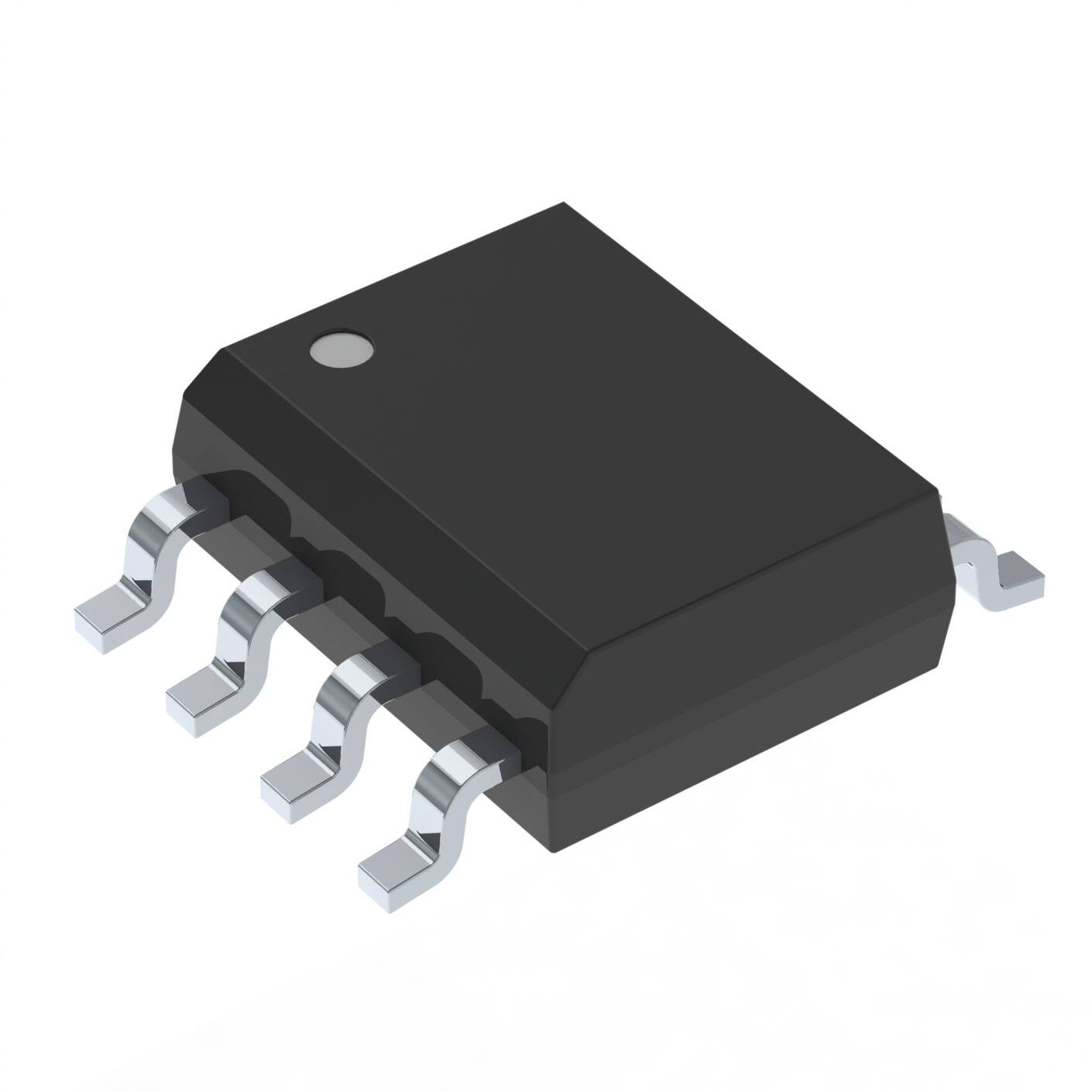
AUIR3241S
Automotive grade
LOW QUIESCENT CURRENT BACK TO BACK MOSFET DRIVER
Features
Very low quiescent current on and off state
Back to back configuration
Boost converter with integrated diode
Standard level gate voltage
Input active high and 3.3V compatible
Under voltage lockout with diagnostic
Wide operating voltage 3-36V
Ground loss protection
Lead-Free, Halogen Free, RoHS compliant
Product Summary
Operating voltage 3-36V
Vgate 11.5V min.
I Vcc average On 45µA max. at 25°C
I Vcc average Off 35µA max. at 25°C
Applications
Power switch for Stop and Start board net stabilizer
Battery switch
Package
SO8
Description
The AUIR3241S is a high side Mosfet driver for back to back topology targeting back to back switch. It features a very low
quiescent current both on and off state. The AUIR3241S is a combination of a boost DC/DC converter using an external inductor
and a gate driver. It drives standard level Mosfet even at low battery voltage. The input controls the gate voltage. The AUIR3241S
integrates an under voltage lock out protection to prevent to drive the Mosfet in linear mode.
Ordering Information
Base Part Number
Standard Pack
Package Type
Complete Part Number
Form
AUIR3241S
1
Rev 1.01
SOIC8
Tape and reel
Quantity
2500
AUIR3241STR
2017-09-12
�AUIR3241S
Typical Connection – Back to Back
Main Battery
Loads
Out
Cout
AUIR3241S
VCC
Cin
Gate
Rg
IN
18V
Source
Rin
Sw
100µH
Current measurement
Rs
GND
Rs
Typical Connection – Q_diode
Main Battery
Loads
Out
Cout
AUIR3241S
VCC
Cin
Gate
Rg
IN
18V
Source
Rin
Sw
100µH
Current measurement
Rs
GND
Rs
2
Rev 1.01
2017-09-12
�AUIR3241S
Typical Connection – Battery switch
Main Battery
Loads
Out
Cout
AUIR3241S
VCC
Cin
Gate
Rg
IN
18V
Source
Rin
Sw
100µH
Current measurement
Rs
GND
Rs
3
Rev 1.01
2017-09-12
�AUIR3241S
Absolute Maximum Ratings
Absolute maximum ratings indicate sustained limits beyond which damage to the device may occur.
Symbol
Parameter
Vcc-gnd
Vsw-gnd
Vsw-Vrs
Vout-Vcc
Vout-gnd
Vout-Vgate
Vgate-Vsource
Vout-Vsource
Vrs-gnd
Vin-gnd
Isw
ID
Rg
Maximum Vcc voltage
Maximum Sw voltage
Maximum Sw voltage
Maximum Vout-Vcc voltage
Maximum Vout voltage
Maximum Vout-Vgate voltage
Maximum Vgate-Vsource voltage
Maximum Vout-Vsource voltage
Maximum Rs pin voltage
Maximum IN pin voltage
Maximum continuous current in Sw pin
Maximum continuous current in the rectifier diode
Minimum gate resistor
Maximum operating junction temperature
Maximum storage temperature
Tj max.
Min.
Max.
-0.3
Vrs-0.3
-0.3
-0.3
-0.3
-0.3
-0.3
-0.3
-0.3
-0.3
65
Vout+Vf
65
65
65
65
75
75
6
Vout+0.3
200
200
Units
100
-40
-55
Ohm
150
150
°C
V
mA
Thermal Characteristics
Symbol
Parameter
Rth
Thermal resistance junction to ambient
Typ.
Max.
Units
100
°C/W
Min.
Max.
Units
2.5
0
5.5
0.8
Recommended Operating Conditions
Symbol
Parameter
VIH
VIL
High level input voltage
Low level input voltage
4
Rev 1.01
V
2017-09-12
�AUIR3241S
Static Electrical Characteristics
Tj=-40..125°C, Vcc=6..16V (unless otherwise specified), typical value are given for Vcc=14V and Tj=25°C.
Symbol
Parameter
Min.
Typ.
Max.
Units
Test Conditions
Supply voltage range for extended operation (some
Vcc op (ext).
parameters may be downgraded beyond nominal
3
36
V
See page 11
operation)
Vcc op (nom). (1)
Supply voltage range for nominal operation
6
16
Iq Vcc Off (2)
Supply current when Off, Tj=25°C
2
6
Vin=0V,K1/K2 off,
K3 on, Vout-Vcc=14V
Supply current when Off, Tj=125°C
3
8
Iq Vcc On (2)
Supply current when On, Tj=25°C
3
6
Vin=5V,K1/K3 off,
µA
K2 on, Vout-Vcc=14V
Supply current when On, Tj=125°C
4
8
Iq Out Off (2)
Quiescent current on Out pin, Tj=25°C
10
15
Vin=0V,K1/K2 off,
K3 on, Vout-Vcc=14V
Quiescent current on Out pin, Tj=125°C
13
25
Iq Out On (2)
Quiescent current on Out pin, Tj=25°C
12
20
Vin=5V,K1/K3 off,
K2 on, Vout-Vcc=14V
Quiescent current on Out pin, Tj=125°C
15
30
Vbr Out
Breakdown voltage between Out and Source
75
90
I=10mA
Vbr Gate
Breakdown voltage between Gate and Source
75
90
V
I=10mA
OV
Over-voltage protection between Vout and Gnd
50
55
62
Iin
Input current
3
6
µA
Vin=5V
Vin_th
Input voltage threshold
0.8
1.5
2.5
Vout_th
Output voltage threshold
11.5
12.5
14
UV_LO
Undervoltage lockout between Vout and Vcc
6.5
8
10
V
See figure 7
Vout_th–UV_LO
Output voltage minus Undervoltage lockout threshold
3
4.5
Vrs th
Rs threshold
0.8
1
1.3
I latch UV_LO
Under voltage lockout Latch current between Vout and
10
25
40
See page 11
mA
Vcc
Vf
Forward voltage of rectifier diode
0.9
1.1
V
I=100mA, Tj=25°C
Rdson K1
Rdson of K1, Tj=-40°C
8
13
I=100mA,
Vout-Vcc=12.5V
Rdson of K1, Tj=25°C
11
15
Rdson of K1, Tj=125°C
15
20
Rdson K2
Rdson of K2, Tj=25°C
25
I=100mA
Rdson K3
Rdson of K3, Tj=25°C
25
(1)
If the part is supply outside of this range (ex: during ramp up of Vcc), other values in this table might not be guaranteed
(2)
Supply current might be higher than specified during the start-up of the part (especially during the charge of Cout)
Timing Converter Characteristics
Tj=-40..125°C, Vcc=6..16V (unless otherwise specified), typical value are given for Vcc=14V and Tj=25°C.
Symbol
Parameter
Toff
Tdon K1
Tdoff K1
POR_Delay
POR_Th
Off time
Turn-on delay of K1
Turn-off delay of K1
Power On Reset delay
Power On Reset threshold
Min.
Typ.
Max.
2
3
5
0.2
500
6.5
4
200
6
1200
7.5
Units
Test Conditions
See figure 4
µs
See figure 5
See figure 10
V
Switching Characteristics
Tj=-40..125°C, Vcc=6..16V (unless otherwise specified), typical value are given for Vcc=14V and Tj=25°C.
Symbol
Parameter
Tdon gate
Tr gate
Igate+
Tdoff gate
Tf gate
IgateTreset
Turn-on delay
Rise time on gate 10% to 90% of Vout-Vcc
Gate high short circuit pulsed current
Turn-off delay
Fall time on gate 90% to 10% of Vout-Vcc
Gate low short circuit pulsed current
Time to reset the under voltage latches
5
Rev 1.01
Min.
Typ.
Max.
Units
0.5
1. 5
6
350
2
6
350
1
3
15
µs
mA
5
15
µs
100
0.5
100
100
mA
µs
Test Conditions
Cgate=100nF
Vgate-Vsource=0V
Cgate=100nF
Vgate-Vsource=14V
See page 11
2017-09-12
�AUIR3241S
Lead Definitions
Pin number
Symbol
1
2
3
4
5
6
7
8
IN
GND
RS
SW
Source
Gate
Vcc
Out
Description
Input pin
Ground pin
Current sense input pin
Output of K1
Connection of the source pin of the Mosfets
Output of the gate driver
Power supply
Output of the boost converter
Lead Assignments
8765
1234
SO8
6
Rev 1.01
1- IN
2- GND
3- RS
4- SW
5- Source
6- Gate
7- Vcc
8- Out
2017-09-12
�AUIR3241S
Block diagram
Vcc
Out
Vout-VccVout_th
UV_LO Latch
S
Q
S
Q
R
Q
R
Q
25mA
75V
K2
+
Vcc
Gate
Vout_th
Power On Reset
75V
75V
75V
D
75V
K3
75V
Source
SW
100µH
K1
Vout>OV
IN
75V
10k
6V
3µs
+
Rs
10k
1V
-
6V
150k
75V
1.5M
toff
Gnd
Input Circuitry
The input control circuitry drives the output gate driver stage. The input is active high. With a low level input voltage, the gate is shorted to the
source. With a high level input, the output gate driver turn on when Vout reaches Vout_th.
Vin
Vgate - Vsource
90%
10%
Tdon gate Tr gate
Figure 1
7
Rev 1.01
2017-09-12
�AUIR3241S
Description
The topology of the AUIR3241S is a boost DC/DC converter working in current mode. The DC/DC is working once the AUIR3241S is powered
regardless the input level.
K1 is switched on when the gate voltage is lower than Vout threshold. When Rs pin reaches Vrs th, K1 is turned off and the inductor charges the
Out capacitor through D. The system cannot restart during Toff after Vrs th has been reached. The DC/DC restart only when the Out and the
Vcc voltage difference is lower than Vout_th in order to achieve low quiescent current on the power supply.
To turn off the power Mosfet, the input must be low. Then K2 is turned off and K3 shorts the gate to the source.
Vcc
Ipeak
Irs
Vout_th
Vout-Vcc
Figure 2
Parameters definition
Current definition
Iq Out Off
Iq Out On
Out
Iq Vcc Off
Iq Vcc On
VCC
GATE
Iq gate
IN
Source
SW
RS
GND
Figure 3
8
Rev 1.01
2017-09-12
�AUIR3241S
Timing definition
Vcc
T
Ipeak
Ik1
Toff
Vout peak
Vout_th
Vout-Vcc
Ipeak
IL
tdischarge
ton
Figure 4
Vout_th
Vout-Vcc
Tdon K1
Tdoff K1
Vrs th
Vrs
Figure 5
Low quiescent current operation when On.
The AUIR3241S is able to operate with a very low quiescent current on the Vcc pin. Nevertheless the supply current depends also on the
leakage of the power mosfet named “Iq gate” on the diagram below.
The leakage current is given when K1 is off. When K1 is on, the current flowing in Vcc is the current charging the inductor. Therefore the
average current on the Vcc is the combination of the current when K1 is ON and OFF. The average current on the Vcc pin can be calculated
using:
Vout − Vcc + Vf
+ Iq Vcc on + Iq Out on
Vcc
Vout − Vcc + Vf
I Vcc average off = (Iq gate + Iq Out Off) ∗
+ Iq Vcc off + Iq Out off
Vcc
I Vcc average on = (Iq gate + Iq Out On) ∗
With Vout: the average voltage on the output.
Vout average = (Vout peak + Vout th)/2
Vout peak can be calculated by:
L
Vout peak = √
. Ipeak 2 + Vout th2
Cout
9
Rev 1.01
2017-09-12
�AUIR3241S
During On operation, the DC/DC works in pulse mode, meaning each time the Vout-Vcc voltage comes below 12.5V, the AUIR3241S switches
on K1 to recharge the gate voltage. When the Iout leakage is low enough to maintain the DC/DC in discontinuous mode, the frequency is
calculate by:
T=
Ipeak2 ∗L
2∗(Iq gate+Iq Vout on)∗(Vout−Vcc+Vf)
Peak current control
The current in the inductor is limited by the 1V comparator which monitors the voltage across Rs. Due to the delay in the loop (tdoff K1), the
inductor current will exceed the threshold set by:
Vrsth
Rs
At low voltage, the current waveform in the inductor is not anymore linear, but exponential because the sum of the resistor of K1, the inductor
and RS are not any more negligible.
Vrs_th
Vrs
t Vrs_th
tdoff K1
t on
Figure 6
The peak current and ton can be calculated as follow:
L
Rs + Rdson k1 + Rl
∗ ln(1 −
)
Rdon k1 + Rs + Rl
Vrs_th ∗ Rs ∗ Vcc
Where Rl is the resistor of the inductor
t Vrsth = −
With : t on = t Vrs_th + tdoff K1
The peak current can be solved by:
Rdson k1+Rs+Rl
Vcc
L
Ipeak =
∗ (1 − e−ton∗
)
Rdson k1 + Rs + Rl
The peak current must not exceed the Maximum Rating of Isw.
10
Rev 1.01
2017-09-12
�AUIR3241S
Output capacitor choice
The output capacitor must be chosen based on 2 criteria:
During the turn on of K2, the voltage drop on Cout must not trigger the Under Voltage Lockout due to the gate charge of the Power
Mosfet.
Cout >
-
Q gate total Power Mosfet
(Voutth –UVLO ) Min.
When K1 turn off and the inductor is charging Cout, the peak current on the output capacitor must be limited in order to avoid having
current flowing in the Gate zener diode:
Cout >
L ∗ Ipeak 2 max
Vz min gate ² − Vout th max²
Vz min gate is the minimum Zener voltage of the external gate Zener diode.
Minimum operating voltage
While the AUIR3241S operating voltage is specified between 3V and 36V. The 3V minimum operating voltage is when the Vcc is going down.
The minimum voltage is also limited by the fact that the Rs voltage must reach the Vrsth taking account all resistors which limit the inductor
current.
Rdson k1 + Rs + Rl
Vcc min =
∗ Vrsth
Rs
Over-Voltage protection
The AUIR3241S integrates an over-voltage protection in order to protect K1. When Vcc exceed the Over-voltage threshold, the DC/DC is
stopped.
Under voltage lockout - Diagnostic
In order to avoid to drive the Power Mosfet in linear mode, the AUIR3241S features an under voltage lockout. During the turn on, the gate will
not be powered until Vout-Vcc reaches Vout th, meaning K2 is off and K3 is on. Then the AUIR3241S powers the gate of the mosfet. If Vout-Vcc
goes below UV_LO, the gate is shorted to the source and the part is latched. A cycle in the input is required to reset the latch. The input must be
kept low longer than Treset.
Vin
Vout-Vcc
Vout_th
UV_LO
Vgate - Vsource
Vout_th
Vrs
Normal Operation
Short on the Gate
Figure 7
When the part is latched a current source (I latch UV_LO) is connected between Out and Vcc to increase the current consumption. By
monitoring the current consumption the system can have a diagnostic of the output status. The diagnostic can be analog or digital.
11
Rev 1.01
2017-09-12
�AUIR3241S
Analog Diagnostic: Output current measurement
The average current into Rs can be measured by adding a low pass filter before the ADC of the micro controller.
Current measurement
Rs
GND
Rs
Figure 8
Then the average output current can be evaluated using :
I out av = I Rs av * Vcc / ( Vout - Vcc )
Knowing the output current can be useful to do a diagnostic on the power Mosfet. If the gate is shorted, the output current will be significantly
higher than in normal operation.
Digital diagnostic
By adding a diode during high current consumption mode, the output voltage can be close to 1V. Using a bipolar with a pull-up resistor will
provide a digital diagnostic.
5V
Digital diagnostic
Rs
GND
Rs
Figure 9
Power On Reset
During the power on, the AUIR3241S features a Power On Reset to guarantee a stable state of the 2 latches of the Under voltage lockout and
guarantee a stable internal biasing. POR_Delay is triggered when Vout-Gnd exceeds POR_Th.
Vin
Vcc
Vout
Vout_th
POR_Th
Vgate - Vsource
POR_Delay
Figure 10
12
Rev 1.01
2017-09-12
�AUIR3241S
Figures are given for typical value, Vcc=14V and Tj=25°C otherwise specified
5
Iq Vcc on, supply leakage current (µA)
Iq Vcc on, supply leakage current (µA)
4
3
2
1
0
0
50
100
2
1
150
0
10
20
30
Tj, junction temperature (°C)
Vcc, Supply voltage (V)
Figure 11 – Iq Vcc on (µA) Vs Tj (°C)
Figure 12 – Iq Vcc on (µA) Vs Vcc(V)
40
20
Iq Out on, Gate leakage current (µA)
20
Iq Out on, Gate leakage current (µA)
3
0
-50
15
10
5
0
15
10
5
0
-50
13
4
0
50
100
150
0
10
20
30
Tj, junction temperature (°C)
Vcc, Supply voltage (V)
Figure 13 – Iq Out on (µA) Vs Tj (°C)
Figure 14 – Iq Out on (µA) Vs Vcc(V)
Rev 1.01
40
2017-09-12
�AUIR3241S
5
Iq Vcc off, supply leakage current (µA)
Iq Vcc off, supply leakage current (µA)
4
3
2
1
0
0
50
100
2
1
150
0
10
20
30
Tj, junction temperature (°C)
Vcc, Supply voltage (V)
Figure 15 – Iq Vcc off (µA) Vs Tj (°C)
Figure 16 – Iq Vcc off (µA) Vs Vcc(V)
40
15
Iq Out off, Gate leakage current (µA)
15
Iq Out off, Gate leakage current (µA)
3
0
-50
10
5
0
10
5
0
-50
14
4
0
50
100
150
0
10
20
30
Tj, junction temperature (°C)
Vcc, Supply voltage (V)
Figure 17 – Iq Out off (µA) Vs Tj (°C)
Figure 18 – Iq Out off (µA) Vs Vcc(V)
Rev 1.01
40
2017-09-12
�AUIR3241S
Case Outline – SO8
15
Rev 1.01
2017-09-12
�AUIR3241S
Tape & Reel
16
SO8
Rev 1.01
2017-09-12
�AUIR3241S
Part Marking Information
Qualification Information
Automotive
(per AEC-Q100)
Comments: This family of ICs has passed an Automotive
qualification. IR’s Industrial and Consumer qualification level
is granted by extension of the higher Automotive level.
Qualification Level
Moisture Sensitivity Level
ESD
Human Body Model
Charged Device Model
IC Latch-Up Test
RoHS Compliant
17
Rev 1.01
SOIC-8L
MSL2, 260°C
(per IPC/JEDEC J-STD-020)
Class 1C Passed 1500V
(per AEC-Q100-002)
Class C6 (+/-1000V)
(per AEC-Q100-011)
Class II Level A
(per AEC-Q100-004)
Yes
2017-09-12
�AUIR3241S
Published by
Infineon Technologies AG
81726 München, Germany
© Infineon Technologies AG 2015
All Rights Reserved.
IMPORTANT NOTICE
The information given in this document shall in no event be regarded as a guarantee of conditions or
characteristics (“Beschaffenheitsgarantie”). With respect to any examples, hints or any typical values stated herein
and/or any information regarding the application of the product, Infineon Technologies hereby disclaims any and all
warranties and liabilities of any kind, including without limitation warranties of non-infringement of intellectual
property rights of any third party.
In addition, any information given in this document is subject to customer’s compliance with its obligations stated in
this document and any applicable legal requirements, norms and standards concerning customer’s products and
any use of the product of Infineon Technologies in customer’s applications.
The data contained in this document is exclusively intended for technically trained staff. It is the responsibility of
customer’s technical departments to evaluate the suitability of the product for the intended application and the
completeness of the product information given in this document with respect to such application.
For further information on the product, technology, delivery terms and conditions and prices please contact your
nearest Infineon Technologies office (www.infineon.com).
WARNINGS
Due to technical requirements products may contain dangerous substances. For information on the types in
question please contact your nearest Infineon Technologies office.
Except as otherwise explicitly approved by Infineon Technologies in a written document signed by authorized
representatives of Infineon Technologies, Infineon Technologies’ products may not be used in any applications
where a failure of the product or any consequences of the use thereof can reasonably be expected to result in
personal injury.
18
Rev 1.01
2017-09-12
�AUIR3241S
Revision History
Revision
Date
Notes/Changes
Rev 1.0
Rev 1.01
2017-04-27
2017-09-12
Data Sheet created.
Update drawing, Differentiate Vcc_op (ext) & Vcc_op
(nom), add Appendixies (1) & (2) on Page 5
19
Rev 1.01
2017-09-12
�


 工商网监
湘ICP备2023018690号
工商网监
湘ICP备2023018690号
