BSO204P
OptiMOS -P Power-Transistor
TM
Product Summary
Feature
• Dual P-Channel
• Enhancement mode
• Super Logic Level (2.5 V rated)
• 150°C operating temperature
• Avalanche rated
• dv/dt rated
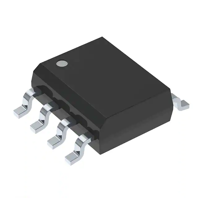
Package
BSO204P
P-SO 8
-20
V
RDS(on)
30
mΩ
ID
-7
A
S1
1
8
D1
G1
2
7
D1
S2
3
6
D2
G2
4
5
D2
Top View
Type
VDS
SIS00070
Maximum Ratings,at Tj = 25 °C, unless otherwise specified
Parameter
Symbol
Continuous drain current
ID
Value
Unit
A
TA=25°C
-7
TA=70°C
-5.6
ID puls
-28
EAS
63
mJ
dv/dt
-6
kV/µs
Gate source voltage
VGS
±12
V
Power dissipation
Ptot
2
W
-55... +150
°C
Pulsed drain current
TA=25°C
Avalanche energy, single pulse
ID =-7 A , VDD=-10V, RGS =25Ω
Reverse diode dv/dt
IS =-7A, VDS=-16V, di/dt=200A/µs, Tjmax =150°C
TA=25°C
Tj , Tstg
Operating and storage temperature
IEC climatic category; DIN IEC 68-1
Rev.1.2
55/150/56
Page 1
2001-12-03
�BSO204P
Thermal Characteristics
Symbol
Parameter
Values
Unit
min.
typ.
max.
-
-
50
@ min. footprint, t < 10s
-
-
110
@ 6 cm 2 cooling area
-
-
62.5
Characteristics
Thermal resistance, junction - soldering point
RthJS
SMD version, device on PCB:
RthJA
1)
K/W
Electrical Characteristics, at Tj = 25 °C, unless otherwise specified
Parameter
Symbol
Values
Unit
min.
typ.
max.
V(BR)DSS
-20
-
-
VGS(th)
-0.6
-0.9
-1.2
Static Characteristics
Drain-source breakdown voltage
V
VGS =0V, ID =-250µA
Gate threshold voltage, VGS = VDS
ID =-60µA
IDSS
Zero gate voltage drain current
µA
VDS =-20V, VGS =0, Tj =25°C
-
-0.1
-1
VDS =-20V, VGS =0, Tj =150°C
-
-10
-100
IGSS
-
-10
-100
nA
RDS(on)
-
34
42
mΩ
RDS(on)
-
23.7
30
Gate-source leakage current
VGS =-12V, VDS =0
Drain-source on-state resistance
VGS =-2.5V, ID =-6.1A
Drain-source on-state resistance
VGS =-4.5, ID =-7A
1Device on 40mm*40mm*1.5mm epoxy PCB FR4 with 6cm2 (one layer, 70 µm thick) copper area for drain
connection. PCB is vertical without blown air; t ≤10 sec.
Rev.1.2
Page 2
2001-12-03
�BSO204P
Electrical Characteristics, at Tj = 25 °C, unless otherwise specified
Parameter
Symbol
Conditions
Values
Unit
min.
typ.
max.
12.5
25
-
S
pF
Dynamic Characteristics
Transconductance
gfs
çVDS ç≥2*çIDç*RDS(on)max
ID =-5.6A
Input capacitance
Ciss
VGS =0, VDS =-15V,
-
1513
-
Output capacitance
Coss
f=1MHz
-
567
-
Reverse transfer capacitance
Crss
-
469
-
Turn-on delay time
td(on)
VDD =-10V, VGS =-4.5V,
-
12.9
19.4
Rise time
tr
ID =-1A, RG=6Ω
-
20.5
30.7
Turn-off delay time
td(off)
-
40.6
61
Fall time
tf
-
35.3
52.4
-
-2.7
-4
-
-11.3
-16.9
-
-23.9
-35.8
V(plateau) VDD =-15V, ID =-7A
-
-1.7
-
V
IS
-
-
-2.5
A
-
-
-28
ns
Gate Charge Characteristics
Gate to source charge
Qgs
Gate to drain charge
Qgd
Gate charge total
Qg
VDD =-15V, ID =-7A
VDD =-15V, ID =-7A,
nC
VGS =0 to -4.5V
Gate plateau voltage
Reverse Diode
Inverse diode continuous
TA=25°C
forward current
Inverse diode direct current,
ISM
pulsed
Inverse diode forward voltage
VSD
VGS =0, IF=-7A
-
-0.87
-1.35 V
Reverse recovery time
trr
VR =-10V, |IF | = |lD |,
-
28.7
35.9
ns
Reverse recovery charge
Qrr
diF /dt=100A/µs
-
14.5
18.1
nC
Rev.1.2
Page 3
2001-12-03
�BSO204P
1 Power dissipation
2 Drain current
Ptot = f (TA )
ID = f (TA )
parameter: |VGS |≥ 4.5 V
2.2
BSO204P
BSO204P
-7.5
A
W
1.8
-6
-5.5
-5
1.4
ID
Ptot
1.6
-4.5
1.2
-4
1
-3.5
-3
0.8
-2.5
0.6
-2
0.4
-1.5
-1
0.2
-0.5
0
0
20
40
60
80
100
120
°C
0
0
160
20
40
60
80
100
120
TA
3 Transient thermal impedance
ZthJS = f (tp)
ID = f ( VDS )
parameter : D = tp /T
parameter : D = 0 , TA = 25 °C
BSO204P
=
RD
o
S(
VD
BSO204P
K/W
S
tp = 180.0µs
10 1
n)
1
Z thJS
1 ms
ID
-10
10 2
/I D
A
160
TA
4 Safe operating area
-10 2
°C
10 0
10 ms
10 -1
-10 0
D = 0.50
0.20
10
-2
0.10
0.05
-10
-1
0.02
DC
10 -3
0.01
single pulse
-10 -2 -1
-10
-10
0
-10
1
V
-10
2
VDS
Rev.1.2
Page 4
10 -4 -7
10
10
-6
10
-5
10
-4
10
-3
10
-2
s
10
tp
2001-12-03
0
�BSO204P
5 Typ. output characteristic
6 Typ. drain-source on resistance
ID = f (VDS ); Tj=25°C
RDS(on) = f (ID )
parameter: tp = 80 µs
parameter: VGS
0.1
30
Vgs = -2.5V
Ω
Vgs = -2.5V
A
RDS(on)
- ID
0.08
Vgs = -2.8V
Vgs = -3V
Vgs = -3.5V
Vgs = -4.5V
Vgs = -6V
20
15
0.07
0.06
0.05
Vgs= -2.8
Vgs= -3
Vgs= -3.5
Vgs = - 4.5V
Vgs= - 6V
0.04
10
0.03
0.02
5
0.01
0
0
0.5
1
1.5
V
2
0
0
3
5
10
15
20
A
- V DS
30
- ID
7 Typ. transfer characteristics
8 Typ. forward transconductance
ID= f ( VGS ); |VDS |≥ 2 x |ID| x RDS(on)max
gfs = f(ID); Tj=25°C
parameter: tp = 80 µs
parameter: tp = 80 µs
45
28
A
S
24
22
35
30
18
gfs
- ID
20
16
25
14
20
12
10
15
8
10
6
4
5
2
0
0
0.5
1
1.5
V
2.5
- V GS
Rev.1.2
0
0
5
10
15
20
A
30
- ID
Page 5
2001-12-03
�BSO204P
9 Drain-source on-resistance
10 Gate threshold voltage
RDS(on) = f(Tj )
VGS(th) = f (Tj)
parameter: ID = -7 A, VGS = -4.5 V
parameter: VGS = VDS , ID = -60 µA
45
1.6
V
- VGS(th)
RDS(on)
mΩ
35
98%
30
1.2
98%
1
0.8
typ.
0.6
25
typ.
2%
0.4
20
0.2
15
-60
-20
20
60
100
°C
0
-60
160
-20
20
60
100
Tj
°C
160
Tj
11 Typ. capacitances
12 Forward character. of reverse diode
C = f (VDS)
IF = f (VSD)
parameter: VGS =0, f=1 MHz
parameter: Tj , tp = 80 µs
10
4
-10 2
BSO204P
A
pF
Ciss
C
IF
-10 1
10 3
Coss
-10 0
Tj = 25 °C typ
Crss
Tj = 150 °C typ
Tj = 25 °C (98%)
Tj = 150 °C (98%)
10 2
0
5
10
V
20
- VDS
Rev.1.2
-10 -1
0
-0.4
-0.8
-1.2
-1.6
-2
-2.4 V
-3
VSD
Page 6
2001-12-03
�BSO204P
13 Typ. avalanche energy
14 Typ. gate charge
EAS = f (Tj ), par.: ID = -7 A
|VGS| = f (QGate )
VDD = -10 V, RGS = 25 Ω
parameter: ID = -7 A pulsed
65
mJ
12
V
55
10
9
- VGS
E AS
50
45
40
8
7
35
0.2 VDS max.
0.5 VDS max.
0.8 VDS max.
6
30
5
25
4
20
3
15
10
2
5
1
0
25
50
75
100
°C
150
Tj
0
0
5
10
15
20
25
30
35
40 nC
50
|QGate|
15 Drain-source breakdown voltage
V(BR)DSS = f (Tj )
-24.5
BSO204P
V
V (BR)DSS
-23.5
-23
-22.5
-22
-21.5
-21
-20.5
-20
-19.5
-19
-18.5
-18
-60
-20
20
60
100
°C
180
Tj
Rev.1.2
Page 7
2001-12-03
�BSP204P
Rev.1.2
Page 8
2001-12-03
�