BTS50025-1TEA
Smart Hig h-Side Power Switch
1
Overview
Features
•
One channel device
•
Low Stand-by current
•
Current controlled input
•
Reverse battery protection
•
Electrostatic discharge protection (ESD)
•
Optimized Electromagnetic Compatibility (EMC)
•
Compatible to cranking pulses (Severe cold start E11 in LV124)
•
Embedded diagnostic functions
•
Embedded protection functions
•
Green Product (RoHS compliant)
Applications
•
Suitable for resistive, inductive and capacitive loads
•
Replaces electromechanical relays, fuses and discrete circuits
•
Most suitable for application with high current loads, such heating system, fan and pump
•
PWM applications with low frequency
Product validation
Qualified for automotive applications. Product validation according to AEC-Q100.
Description
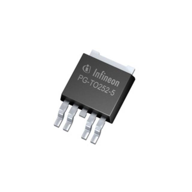
The BTS50025-1TEA is a 2.5mΩ single channel Smart High-Side Power Switch, embedded in a PG-TO-252-5-11
package, providing protective functions and diagnosis. It contains Infineon® ReverSave™ functionality. The
power transistor is built by an N-channel MOSFET with charge pump. It is specially designed to drive high
current loads up to 65A, for application like heaters, glow plugs, fan and pump in the harsh automotive
environment.
Data Sheet
www.infineon.com
1
Rev.1.1
2019-09-30
�BTS50025-1TEA
Smart High-Side Power Switch
Overview
Table 1
Product Summary
Parameter
Symbol
Values
Operating Voltage
VS(OP)
5.8 V … 18 V
Extended supply voltage range
VS(EXT)
3.1 V ...27 V
Maximum ON-State Resistance (Tj = 150 °C)
RDS(ON)
5 mΩ
Nominal Load Current (TA = 85°C)
IL(NOM)
24 A
Typical current sense differential ratio
dkILIS
18000
Minimum short circuit current threshold
ICL(0)
65 A
Maximum reverse battery voltage
-VS(REV)
-16 V
Maximum Stand-by Current at Tj = 25 °C
Ivs(off)
4 µA
Embedded Diagnostic Functions
•
Proportional load current sense
•
Short circuit / Overtemperature detection
•
Latched status signal after short circuit or overtemperature detection
Embedded Protection Functions
•
Infineon® ReverSave™: Reverse battery protection by self turn ON of power MOSFET
•
Short circuit protection with latch
•
Overtemperature protection with latch
•
Enhanced short circuit operation
•
Infineon® SMART CLAMPING
Type
Package
Marking
BTS50025-1TEA
PG-TO-252-5-11
S50025A
Data Sheet
2
Rev.1.1
2019-09-30
�BTS50025-1TEA
Smart High-Side Power Switch
Table of Contents
1
Overview . . . . . . . . . . . . . . . . . . . . . . . . . . . . . . . . . . . . . . . . . . . . . . . . . . . . . . . . . . . . . . . . . . . . . . . . 1
Features . . . . . . . . . . . . . . . . . . . . . . . . . . . . . . . . . . . . . . . . . . . . . . . . . . . . . . . . . . . . . . . . . . . . . . . . 1
Applications . . . . . . . . . . . . . . . . . . . . . . . . . . . . . . . . . . . . . . . . . . . . . . . . . . . . . . . . . . . . . . . . . . . . . 1
Product validation . . . . . . . . . . . . . . . . . . . . . . . . . . . . . . . . . . . . . . . . . . . . . . . . . . . . . . . . . . . . . . . . 1
Description . . . . . . . . . . . . . . . . . . . . . . . . . . . . . . . . . . . . . . . . . . . . . . . . . . . . . . . . . . . . . . . . . . . . . . 1
Table of Contents . . . . . . . . . . . . . . . . . . . . . . . . . . . . . . . . . . . . . . . . . . . . . . . . . . . . . . . . . . . . . . . . . 3
List of Tables . . . . . . . . . . . . . . . . . . . . . . . . . . . . . . . . . . . . . . . . . . . . . . . . . . . . . . . . . . . . . . . . . . . . 5
List of Figures . . . . . . . . . . . . . . . . . . . . . . . . . . . . . . . . . . . . . . . . . . . . . . . . . . . . . . . . . . . . . . . . . . . . 6
2
Block Diagram . . . . . . . . . . . . . . . . . . . . . . . . . . . . . . . . . . . . . . . . . . . . . . . . . . . . . . . . . . . . . . . . . . . 7
3
3.1
3.2
3.3
Pin Configuration . . . . . . . . . . . . . . . . . . . . . . . . . . . . . . . . . . . . . . . . . . . . . . . . . . . . . . . . . . . . . . . . . 8
Pin Assignment 8
Pin Definitions and Functions 8
Voltage and Current Definition 9
4
4.1
4.2
4.3
General Product Characteristics . . . . . . . . . . . . . . . . . . . . . . . . . . . . . . . . . . . . . . . . . . . . . . . . . . . 10
Absolute Maximum Ratings 10
Functional Range 13
Thermal Resistance 14
5
5.1
5.1.1
5.1.2
5.1.3
5.1.3.1
5.1.3.2
5.1.4
5.1.5
5.2
5.2.1
5.3
5.3.1
5.3.1.1
5.3.1.2
5.3.1.3
5.3.2
5.4
5.4.1
5.4.2
5.4.3
5.4.3.1
5.4.3.2
5.4.3.3
5.4.3.4
Functional Description . . . . . . . . . . . . . . . . . . . . . . . . . . . . . . . . . . . . . . . . . . . . . . . . . . . . . . . . . . .
Power Stage 15
Output ON-State Resistance . . . . . . . . . . . . . . . . . . . . . . . . . . . . . . . . . . . . . . . . . . . . . . . . . . . . . . . . . . . .
Switching Resistive Loads . . . . . . . . . . . . . . . . . . . . . . . . . . . . . . . . . . . . . . . . . . . . . . . . . . . . . . . . . . . . . .
Switching Inductive Loads . . . . . . . . . . . . . . . . . . . . . . . . . . . . . . . . . . . . . . . . . . . . . . . . . . . . . . . . . . . . . .
Output Clamping . . . . . . . . . . . . . . . . . . . . . . . . . . . . . . . . . . . . . . . . . . . . . . . . . . . . . . . . . . . . . . . . . . . .
Maximum Load Inductance . . . . . . . . . . . . . . . . . . . . . . . . . . . . . . . . . . . . . . . . . . . . . . . . . . . . . . . . . . .
PWM Switching . . . . . . . . . . . . . . . . . . . . . . . . . . . . . . . . . . . . . . . . . . . . . . . . . . . . . . . . . . . . . . . . . . . . . . . .
Advanced switch-off behavior . . . . . . . . . . . . . . . . . . . . . . . . . . . . . . . . . . . . . . . . . . . . . . . . . . . . . . . . . . .
Input Pins 19
Input Circuitry . . . . . . . . . . . . . . . . . . . . . . . . . . . . . . . . . . . . . . . . . . . . . . . . . . . . . . . . . . . . . . . . . . . . . . . . .
Protection Functions 19
Overload Protection . . . . . . . . . . . . . . . . . . . . . . . . . . . . . . . . . . . . . . . . . . . . . . . . . . . . . . . . . . . . . . . . . . . .
Activation of the Switch into Short Circuit (Short Circuit Type 1) . . . . . . . . . . . . . . . . . . . . . . . . . .
Short Circuit Appearance when the Device is already ON (Short Circuit Type 2) . . . . . . . . . . . .
Over-power shutdown (PSD) . . . . . . . . . . . . . . . . . . . . . . . . . . . . . . . . . . . . . . . . . . . . . . . . . . . . . . . . . .
Temperature Limitation in the Power DMOS . . . . . . . . . . . . . . . . . . . . . . . . . . . . . . . . . . . . . . . . . . . . . .
Diagnostic Functions 22
IS Pin . . . . . . . . . . . . . . . . . . . . . . . . . . . . . . . . . . . . . . . . . . . . . . . . . . . . . . . . . . . . . . . . . . . . . . . . . . . . . . . . .
SENSE Signal in Different Operation Modes . . . . . . . . . . . . . . . . . . . . . . . . . . . . . . . . . . . . . . . . . . . . . . .
SENSE Signal in the Nominal Current Range . . . . . . . . . . . . . . . . . . . . . . . . . . . . . . . . . . . . . . . . . . . . . .
SENSE Signal Variation and Calibration . . . . . . . . . . . . . . . . . . . . . . . . . . . . . . . . . . . . . . . . . . . . . . . .
SENSE Signal Timing . . . . . . . . . . . . . . . . . . . . . . . . . . . . . . . . . . . . . . . . . . . . . . . . . . . . . . . . . . . . . . . . .
SENSE Signal in Case of Short Circuit to VS . . . . . . . . . . . . . . . . . . . . . . . . . . . . . . . . . . . . . . . . . . . . .
SENSE Signal in Case of Over Load . . . . . . . . . . . . . . . . . . . . . . . . . . . . . . . . . . . . . . . . . . . . . . . . . . . .
Data Sheet
3
15
15
15
15
15
17
18
18
19
20
20
20
20
21
22
23
23
25
27
27
27
Rev.1.1
2019-09-30
�BTS50025-1TEA
Smart High-Side Power Switch
6
6.1
6.2
Electrical Characteristics BTS50025-1TEA . . . . . . . . . . . . . . . . . . . . . . . . . . . . . . . . . . . . . . . . . . . 29
Electrical Characteristics Table 29
Typical Performance Characteristics 35
7
7.1
Application Information . . . . . . . . . . . . . . . . . . . . . . . . . . . . . . . . . . . . . . . . . . . . . . . . . . . . . . . . . . 40
Further Application Information 41
8
Package Information . . . . . . . . . . . . . . . . . . . . . . . . . . . . . . . . . . . . . . . . . . . . . . . . . . . . . . . . . . . . . 42
9
Revision History . . . . . . . . . . . . . . . . . . . . . . . . . . . . . . . . . . . . . . . . . . . . . . . . . . . . . . . . . . . . . . . . . 43
Data Sheet
4
Rev.1.1
2019-09-30
�BTS50025-1TEA
Smart High-Side Power Switch
List of Tables
Table 1
Table 2
Table 3
Table 4
Table 5-1
Table 6-1
Table 7-1
Data Sheet
Product Summary . . . . . . . . . . . . . . . . . . . . . . . . . . . . . . . . . . . . . . . . . . . . . . . . . . . . . . . . . . . . . . . . . . . . . 2
Absolute Maximum Ratings . . . . . . . . . . . . . . . . . . . . . . . . . . . . . . . . . . . . . . . . . . . . . . . . . . . . . . . . . . . . 10
Functional Range . . . . . . . . . . . . . . . . . . . . . . . . . . . . . . . . . . . . . . . . . . . . . . . . . . . . . . . . . . . . . . . . . . . . . 13
Thermal Resistance . . . . . . . . . . . . . . . . . . . . . . . . . . . . . . . . . . . . . . . . . . . . . . . . . . . . . . . . . . . . . . . . . . . 14
Sense Signal, Function of Operation Mode . . . . . . . . . . . . . . . . . . . . . . . . . . . . . . . . . . . . . . . . . . . . . . 23
Electrical Characteristics: BTS50025-1TEA . . . . . . . . . . . . . . . . . . . . . . . . . . . . . . . . . . . . . . . . . . . . . . . 29
Bill of material . . . . . . . . . . . . . . . . . . . . . . . . . . . . . . . . . . . . . . . . . . . . . . . . . . . . . . . . . . . . . . . . . . . . . . . . 41
5
Rev.1.1
2019-09-30
�BTS50025-1TEA
Smart High-Side Power Switch
List of Figures
Figure 2-1
Figure 2-2
Figure 3-1
Figure 3-2
Figure 1
Figure 2
Figure 3
Figure 5-1
Figure 5-2
Figure 5-3
Figure 5-4
Figure 5-5
Figure 5-6
Figure 5-7
Figure 5-8
Figure 5-9
Figure 5-10
Figure 5-11
Figure 5-12
Figure 5-13
Figure 5-14
Figure 7-1
Figure 8-1
Data Sheet
Block Diagram for the BTS50025-1TEA . . . . . . . . . . . . . . . . . . . . . . . . . . . . . . . . . . . . . . . . . . . . . . . . . . . 7
Internal diode diagram . . . . . . . . . . . . . . . . . . . . . . . . . . . . . . . . . . . . . . . . . . . . . . . . . . . . . . . . . . . . . . . . . 7
Pin Configuration . . . . . . . . . . . . . . . . . . . . . . . . . . . . . . . . . . . . . . . . . . . . . . . . . . . . . . . . . . . . . . . . . . . . . . 8
Voltage and Current Definition . . . . . . . . . . . . . . . . . . . . . . . . . . . . . . . . . . . . . . . . . . . . . . . . . . . . . . . . . . 9
Maximum Energy Dissipation for Inductive Switch OFF, EAS/AR vs. IL at VS = 13.5 V . . . . . . . . . . . . 12
Maximum Energy Dissipation Repetitive Pulse temperature derating . . . . . . . . . . . . . . . . . . . . . . . 12
Typical Transient Thermal Impedance Zth(JA) = f(time) for Different PCB Conditions . . . . . . . . . . 14
Switching a Resistive Load: Timing. . . . . . . . . . . . . . . . . . . . . . . . . . . . . . . . . . . . . . . . . . . . . . . . . . . . . . 15
Output Clamp. . . . . . . . . . . . . . . . . . . . . . . . . . . . . . . . . . . . . . . . . . . . . . . . . . . . . . . . . . . . . . . . . . . . . . . . . 16
Switching an Inductance . . . . . . . . . . . . . . . . . . . . . . . . . . . . . . . . . . . . . . . . . . . . . . . . . . . . . . . . . . . . . . . 16
Switching in PWM . . . . . . . . . . . . . . . . . . . . . . . . . . . . . . . . . . . . . . . . . . . . . . . . . . . . . . . . . . . . . . . . . . . . . 18
Input Pin Circuitry . . . . . . . . . . . . . . . . . . . . . . . . . . . . . . . . . . . . . . . . . . . . . . . . . . . . . . . . . . . . . . . . . . . . . 19
Diagram of Diagnosis & Protection Block . . . . . . . . . . . . . . . . . . . . . . . . . . . . . . . . . . . . . . . . . . . . . . . . 20
Over Power Shutdown behavior at low voltage. . . . . . . . . . . . . . . . . . . . . . . . . . . . . . . . . . . . . . . . . . . 21
Behavior of the BTS50025-1TEA during PWM operation above FIN max . . . . . . . . . . . . . . . . . . . . . 21
Overload Protection . . . . . . . . . . . . . . . . . . . . . . . . . . . . . . . . . . . . . . . . . . . . . . . . . . . . . . . . . . . . . . . . . . . 22
Diagnostic Block Diagram . . . . . . . . . . . . . . . . . . . . . . . . . . . . . . . . . . . . . . . . . . . . . . . . . . . . . . . . . . . . . . 23
Current Sense for Nominal and Overload Condition . . . . . . . . . . . . . . . . . . . . . . . . . . . . . . . . . . . . . . 24
IIL0 and IISO definition . . . . . . . . . . . . . . . . . . . . . . . . . . . . . . . . . . . . . . . . . . . . . . . . . . . . . . . . . . . . . . . . . . 25
Improved Current Sense Accuracy after 2-Point Calibration . . . . . . . . . . . . . . . . . . . . . . . . . . . . . . . 26
Fault Acknowledgement . . . . . . . . . . . . . . . . . . . . . . . . . . . . . . . . . . . . . . . . . . . . . . . . . . . . . . . . . . . . . . . 27
Application Diagram with BTS50025-1TEA . . . . . . . . . . . . . . . . . . . . . . . . . . . . . . . . . . . . . . . . . . . . . . . 40
PG-TO-252-5-11 (RoHS-Compliant) . . . . . . . . . . . . . . . . . . . . . . . . . . . . . . . . . . . . . . . . . . . . . . . . . . . . 42
6
Rev.1.1
2019-09-30
�BTS50025-1TEA
Smart High-Side Power Switch
Block Diagram
2
Block Diagram
VS
voltage sensor
over
temperature
driver
logic
IN
ESD
protection
gate control
&
charge
pump
Smart clamp
over current
switch OFF
OUT
load current sense
IS
Figure 2-1 Block Diagram for the BTS50025-1TEA
VCC
75V
2mA
75V
200
35V
IFB OUT
IN
Figure 2-2 Internal diode diagram
Data Sheet
7
Rev.1.1
2019-09-30
�BTS50025-1TEA
Smart High-Side Power Switch
Pin Configuration
3
Pin Configuration
3.1
Pin Assignment
3
1 2
4 5
Figure 3-1 Pin Configuration
3.2
Pin Definitions and Functions
Pin
Symbol Function
1
OUT
OUTput; Protected high side power output channel1)
2
IN
INput; Digital signal to switch ON channel with Bipolar or Mosfet (active “low”)
3, Cooling tab VS
Supply Voltage; Battery voltage
4
IS
Sense; Analog/Digital signal for diagnosis, if not used: left open
5
OUT
OUTput; Protected high side power output channel1)
1) All output pins are internally connected and they also have to be connected together on the PCB. Not shorting all
outputs on PCB will considerably increase the ON-state resistance and decrease the current sense / overcurrent
tripping accuracy. PCB traces have to be designed to withstand the maximum current.
Exact path resistance matching on both outputs to common point is needed also for short circuit robustness and
reliability at high current.
Data Sheet
8
Rev.1.1
2019-09-30
�BTS50025-1TEA
Smart High-Side Power Switch
Pin Configuration
3.3
Voltage and Current Definition
Figure 3-2 shows all terms used in this data sheet, with associated convention for positive values.
I VS
VS
VS
I IN
IN
V DS
I OUT
OUT
VIN
I IS
IS
V OUT
V IS
Figure 3-2 Voltage and Current Definition
Data Sheet
9
Rev.1.1
2019-09-30
�BTS50025-1TEA
Smart High-Side Power Switch
General Product Characteristics
4
General Product Characteristics
4.1
Absolute Maximum Ratings
Table 2
Absolute Maximum Ratings1)
Tj = -40°C to +150°C; (unless otherwise specified)
Parameter
Symbol
Values
Min.
Typ.
Max.
-0.3
–
35
Unit
Note or
Test Condition
Number
V
–
P_4.1.1
2)
P_4.1.2
Supply Voltages
Supply Voltage
VS
Reverse Polarity Voltage
-VS(REV)
0
–
18
V
Vin=0 V
TA = 25°C
RL ≥ 0.68 Ω
t < 5 min.
Load Dump Voltage
VS(LD)
–
–
45
V
P_4.1.3
Suppressed
Load Dump acc.
to ISO16750-2
RI = 2 Ω
td=200ms
Us=100V
RL = 0.68 Ω
RIS = 1 kΩ
VS(LD) = US*
3.1
–
27
V
In accordance to P_4.1.4
AEC Q100-012,
Figure-1 Test
Circuit.
Short Circuit Capability
Supply Voltage for Short Circuit VS(SC)
Protection
Input Pin
Voltage at IN pin
Vs - Vin
-16
–
75
V
–
P_4.1.6
Current through IN pin
IIN
-50
–
50
mA
–
P_4.1.20
Maximum Input Frequency
Fin
–
–
200
Hz
5.8V Fin max
Input frequency < Fin max
Vin-Gnd
t
Vout-Gnd
t
Vifb
t
Normal operation
Missing pulses – Part is latched
Normal operation
Figure 5-8 Behavior of the BTS50025-1TEA during PWM operation above FIN max
5.3.2
Temperature Limitation in the Power DMOS
The BTS50025-1TEA incorporates a temperature sensor. Triggering the over-temperature (TJ(TRIP)) will switch
OFF the Power Mosfet to prevent destruction and latches the device.
Data Sheet
21
Rev.1.1
2019-09-30
�BTS50025-1TEA
Smart High-Side Power Switch
Functional Description
tIN (RESETDELAY)
IN
IL
t OFF ( TRIP )
t
t OFF ( TRIP )
ICL(1)
ICL(0)
T
t
J
T J( TRIP )
TA
t
I IS
I IS(
FAULT)
t
Overtemperature
Short Circuit 1
Latch is reseted
Short Circuit 2
start
0
Figure 5-9 Overload Protection
The current sense exact signal timing can be found in the Chapter 5.4.3.2. It is represented here only for
device’s behavior understanding.
5.4
Diagnostic Functions
For diagnosis purposes, the BTS50025-1TEA provides a combination of digital and analog signal at pin IS.
5.4.1
IS Pin
The BTS50025-1TEA provides an enhanced current sense signal called IIS at pin IS. As long as no “hard” failure
mode occurs (short circuit to GND / overcurrent / overtemperature) and the condition VIS ≤ VOUT - 3.5 V is
fulfilled, a proportional signal to the load current is provided. The complete IS pin and diagnostic mechanism
is described in Figure 5-10. The accuracy of the sense current depends on temperature and load current. In
case of failure, a fixed IIS(FAULT) is provided. In order to get the fault current in the specified range, the condition
VS - VIS ≥ 3.5 V must be fulfilled.
Data Sheet
22
Rev.1.1
2019-09-30
�BTS50025-1TEA
Smart High-Side Power Switch
Functional Description
VS
IIS( FAULT)
ZIS( AZ)
( I L / dk ILIS ) ± IIS(0)
FAULT
1
IS
0
Figure 5-10 Diagnostic Block Diagram
5.4.2
SENSE Signal in Different Operation Modes
Table 5-1
Sense Signal, Function of Operation Mode1)
Operation mode
Input Level
Output Level VOUT
Diagnostic Output (IS)2)
Normal operation
HIGH (OFF)
GND
IIS(OFF)
Short circuit to GND
GND
IIS(OFF)
Overtemperature
GND
IIS(OFF)
Short circuit to VS
VS
IIS(OFF)
Open Load
Z
IIS(OFF)
~ VS
IIS = (IL / dkILIS) ± IIS0
Short circuit to GND
GND
IIS(FAULT)
Overtemperature (after the event)
GND
IIS(FAULT)
Short circuit to VS
VS
IIS < IL / dkILIS ± IIS0
Open Load
VS
IIS0
Normal operation
LOW (ON)
1) Z = High Impedance
2) See Chapter 5.4.3 for Current Sense Range and Improved Current Sense Accuracy.
5.4.3
SENSE Signal in the Nominal Current Range
Figure 5-11 and Figure 5-13 show the current sense as function of the load current in the power DMOS.
Usually, a pull-down resistor RIS is connected to the current sense pin IS. A typical value is 1 kΩ. The dotted
curve represents the typical sense current, assuming a typical dkILIS factor value. The range between the two
solid curves shows the sense accuracy range that the device is able to provide, at a defined current.
IIS =
Data Sheet
IL
+ I with (IIS ≥ 0)
dkILIS IS0
23
(5.3)
Rev.1.1
2019-09-30
�BTS50025-1TEA
Smart High-Side Power Switch
Functional Description
where the definition of dkILIS is:
dkILIS =
IL3 - IL1
IIS3 - IIS1
(5.4)
the definition of IIS0 is:
IIS0 = IIS1 −
IL1
dkILIS
(5.5)
and the definition of IL0 is:
IIL0 = IIL1 − IS1 × dkILIS
(5.6)
5
4.5
dKILIS min.
dKILIS typ.
4
3.5
dKILIS max.
IIS [mA]
3
2.5
2
1.5
1
0.5
0
0
20
40
60
80
IL[A]
Figure 5-11 Current Sense for Nominal and Overload Condition
Data Sheet
24
Rev.1.1
2019-09-30
�BTS50025-1TEA
Smart High-Side Power Switch
Functional Description
0.02
dkILIS(min)
0.015
dkILIS(typ)
IIS0(max)
0.01
dkILIS(max)
IIS [mA]
0.005
IIL0(min)
0
IIL0(max)
-0.005
IIS0(min)
-0.01
-0.015
-0.02
-0.5
-0.4
-0.3
-0.2
-0.1
0
0.1
0.2
0.3
0.4
0.5
IL[A]
Figure 5-12 IIL0 and IISO definition
5.4.3.1
SENSE Signal Variation and Calibration
In some applications, an enhanced accuracy is required around the device nominal current range IL(NOM). To
achieve this accuracy requirement, a calibration on the application is possible. After two point calibration, the
BTS50025-1TEA will have a limited IIS value spread at different load currents and temperature conditions. The
IIS variation can be described with the parameters ∆(dkILIS(cal)) and the ∆IIS0(cal). The blue solid line in
Figure 5-13 is the current sense ratio after the two point calibration at a given temperature. The slope of this
line is defined as follows:
1
dkILIS(cal)
=
IIS(cal)2 − IIS(cal)1
IL(cal)2 − IL(cal)1
(5.7)
The offset is defined as follows:
IIS0(cal) = IIS(cal)1 −
IL(cal)1
IL(cal)2
= IIS(cal)2 −
dkILIS(cal)
dkILIS(cal)
(5.8)
The bluish area in Figure 5-13 is the range where the current sense ratio can vary across temperature and load
current after performing the calibration. The accuracy of the load current sensing is improved and, given a
sense current value IIS (measured in the application), the load current can be calculated as follow, using the
absolute value for ∆(dkILIS(cal)) instead of % values:
(
) (
IL = dkILIS(cal) × 1 + ∆(dkILIS(cal)) × IIS − IIS0(cal) − ∆IIS0(cal)
)
(5.9)
Data Sheet
25
Rev.1.1
2019-09-30
�BTS50025-1TEA
Smart High-Side Power Switch
Functional Description
where dkILIS(cal) is the current sense ratio measured after two-points calibration (defined in Equation (5.7)),
IIS0(cal) is the current sense offset (calculated after two points calibration, see Equation (5.8)), and ∆IIS0(cal) is
the additional variation of the individual offset over life time and temperature. For a calibration at 25°C ∆IIS0(cal)
varies over temperature and life time for all positive ∆IIS0(cal) within the differences of the temperature
dependent Max. limits. All negative ∆IIS0(cal) vary within the differences of the temperature dependent Min.
limits.
For positive IIS0(cal) values (IIS0(cal) > 0):
Max IIS0 (@TJ = 150°C) − Max IIS0 (@TJ = 25°C) ≤ ∆IIS0(cal) ≤ Max IIS0 (@TJ = -40°C) − Max IIS0 (@TJ = 25°C)
(5.10)
For negative IIS0(cal) values (IIS0(cal) < 0):
Min IIS0 (@TJ = 150°C) − Min IIS0 (@TJ = 25°C) ≥ ∆IIS0(cal) ≥ Min IIS0 (@TJ = -40°C) − Min IIS0 (@TJ = 25°C)
(5.11)
Equation (5.9) actually provides four solutions for load current, considering that ∆(dkILIS(cal)) and ∆IIS0(cal) can
be both positive and negative. The load current IL for any sense current IIS will spread between a minimum IL
value resulting from the combination of lowest ∆(dkILIS(cal)) value and highest ∆IIS0(cal) and a maximum IL value
resulting from the combination of highest ∆(dkILIS(cal)) value and lowest ∆IIS0(cal).
IIS
1/dkILIS(min)
ΔdkILIS(cal)
1/dkILIS(cal)
IIS(cal)2
ΔdkILIS(cal)
1/dkILIS(max)
IIS
IIS(cal)1
ΔIIS0(cal)
IIS0(cal)
ΔIIS0(cal)
Min IL
Typ IL
IL(cal)1
Max IL
IL(cal)2
IL
Figure 5-13 Improved Current Sense Accuracy after 2-Point Calibration
Data Sheet
26
Rev.1.1
2019-09-30
�BTS50025-1TEA
Smart High-Side Power Switch
Functional Description
5.4.3.2
SENSE Signal Timing
Figure 5-14 shows the timing during settling and disabling of the sense.
VIN
t OFFtIN( RESETDELAY)
Short/
Overtemp/
.
PSD
t
VOUT
t
IIS
IIS(fault) t
IIS
latch
no
reset
VIN
IL
VIN
tON
t
Short
circuit
t
t
VOUT
t
80 % of
IL static
VOUT
IIS
90 % of
IS static
t
reset
tsIS(ON)
t
t
IIS
tsIS(ON)_90
tsIS(LC)
t
IIS( fault)
IIS
tpIS( FAULT)
t
Figure 5-14 Fault Acknowledgement
5.4.3.3
SENSE Signal in Case of Short Circuit to VS
In case of a short circuit between OUT and VS, a major part of the load current will flow through the short
circuit. As a result, a lower current compared to the nominal operation will flow through the DMOS of the
BTS50025-1TEA, which can be recognized at the current sense signal.
5.4.3.4
SENSE Signal in Case of Over Load
An over load condition is defined by a current flowing out of the DMOS reaching the current over load ICL or the
junction temperature reaches the thermal shutdown temperature TJ(TRIP). Please refer to Chapter 5.3.1 for
details. In that case, the SENSE signal will be IIS(FAULT) when the IN pin stays LOW.
Data Sheet
27
Rev.1.1
2019-09-30
�BTS50025-1TEA
Smart High-Side Power Switch
Functional Description
This is a device with latch functionality. The state of the device will remain and the sense signal will remain on
IIS(FAULT) until a reset signal comes from the IN pin. For example, when a thermal shutdown occurs, even when
the over temperature condition has disappeared, the DMOS can only be reactivated when a reset signal is sent
to the IN pin.
Data Sheet
28
Rev.1.1
2019-09-30
�BTS50025-1TEA
Smart High-Side Power Switch
Electrical Characteristics BTS50025-1TEA
6
Electrical Characteristics BTS50025-1TEA
6.1
Electrical Characteristics Table
Table 6-1
Electrical Characteristics: BTS50025-1TEA
VS =5.8 V to 18 V, Tj = -40°C to +150°C (unless otherwise specified)
For a given temperature or voltage range, typical values are specified at VS = 13.5 V, TJ = 25°C
Parameter
Symbol
Values
Min.
Typ.
Max.
Unit
Note or
Test Condition
Number
Operating and Standby Currents
Standby Current for Whole
Device with Load
IVS(OFF)
–
1
4
µA
1)
VS = 18 V
VOUT = 0 V
Vin = Vs
TJ ≤ 85°C
See Page 35
P_6.1.1
Maximum Standby Current
for Whole Device with Load
IVS(OFF)
–
10
100
µA
VS = 18 V
VOUT = 0 V
Vin = Vs
TJ ≤ 150°C
See Παγε 35
P_6.1.2
ON-State Resistance in
Forward Condition
RDS(ON)
–
4.4
5
mΩ
IL = 20 A
Vs - Vin ≥ 5.8 V
TJ = 150°C
See Παγε 35
P_6.1.3
ON-State Resistance in
Forward Condition
RDS(ON)
–
2.7
–
mΩ
1)
IL = 20 A
Vs - Vin ≥ 5.8 V
TJ = 25°C
P_6.1.4
ON-State Resistance in
Forward Condition, Low
Battery Voltage
RDS(ON)
–
6
20
mΩ
IL = 12 A
Vs - Vin ≥ 3.1 V
TJ = 150°C
P_6.1.5
ON-State Resistance in
Forward Condition, Low
Battery Voltage
RDS(ON)
–
3.5
–
mΩ
1)
IL = 12 A
Vs - Vin ≥ 3.1 V
TJ = 25°C
P_6.1.6
Nominal Load Current
IL(NOM)
24
26
–
A
2)
TA = 85°C
TJ ≤ 150°C
P_6.1.7
Drain to Source Smart
Clamp Voltage VDS(CL) = VS VOUT
VDS(CL)
30
35
45
V
IDS = 10 mA
TJ = 25°C
See Page 37
P_6.1.8
Drain to Source Smart
Clamp Voltage VDS(CL) = VS VOUT
VDS(CL)
35
39
50
V
IDS = 10 mA
TJ = 150°C
See Page 37
P_6.1.9
Fast turn off detection
voltage
VDS(FAST)
–
28
–
V
1)
P_6.1.10
Power Stage
Data Sheet
29
See Page 16
Rev.1.1
2019-09-30
�BTS50025-1TEA
Smart High-Side Power Switch
Electrical Characteristics BTS50025-1TEA
Table 6-1
Electrical Characteristics: BTS50025-1TEA (cont’d)
VS =5.8 V to 18 V, Tj = -40°C to +150°C (unless otherwise specified)
For a given temperature or voltage range, typical values are specified at VS = 13.5 V, TJ = 25°C
Parameter
Symbol
Values
Unit
Note or
Test Condition
Number
Min.
Typ.
Max.
Body diode Forward voltage VF
–
0.6
0.8
V
IOUT = -20A
TJ = 150°C
P_6.1.11
Output Leakage Current
IL(OFF)
–
1
4
µA
1)
VS = 18 V
VOUT = 0 V
Vin = Vs
TJ ≤ 85°C
( 10ms after
VS = VIN )
P_6.1.12
Output Leakage Current
IL(OFF)
–
10
100
µA
VS = 18 V
VOUT = 0 V
Vin = Vs
TJ ≤ 150°C
( 10ms after
VS = VIN )
P_6.1.13
Turn ON Slew Rate
VOUT = 25% to 50% VS
dVON/dt
0.05
0.25
1
V/µs
P_6.1.14
Turn OFF Slew Rate
VOUT = 50% to 25% VS
-dVOFF/dt
0.05
0.25
1
V/µs
RL = 0.68 Ω
VS = 13.5 V
See Figure 5-1
See Page 36
tr
Rising time during turn on
VOUT from 20% to 80% of VS
10
50
150
µs
P_6.1.16
Falling time during turn off tf
VOUT from 80% to 20% of VS
10
50
150
µs
P_6.1.17
Turn ON Time to
VOUT = 20% of VS
tON(DELAY)
10
50
250
µs
P_6.1.18
Turn OFF Time to
VOUT = 80% of VS
tOFF(DELAY)
50
150
450
µs
P_6.1.19
Switch ON Energy
EON
–
5.5
–
mJ
1)
RL = 0.68 Ω
VS = 13.5 V
See Page 37
P_6.1.20
Switch OFF Energy
EOFF
–
4
–
mJ
1)
P_6.1.21
Data Sheet
30
RL = 0.68 Ω
VS = 13.5 V
See Page 37
P_6.1.15
Rev.1.1
2019-09-30
�BTS50025-1TEA
Smart High-Side Power Switch
Electrical Characteristics BTS50025-1TEA
Table 6-1
Electrical Characteristics: BTS50025-1TEA (cont’d)
VS =5.8 V to 18 V, Tj = -40°C to +150°C (unless otherwise specified)
For a given temperature or voltage range, typical values are specified at VS = 13.5 V, TJ = 25°C
Parameter
Symbol
Values
Unit
Min.
Typ.
Max.
Note or
Test Condition
Number
Input Pin
LOW Level Input Voltage
VVS-VIN(L)
2.3
2.7
3.1
V
P_6.1.22
HIGH Level Input Voltage
VVS-VIN(H)
4
4.8
5.8
V
P_6.1.23
Input Voltage Hysteresis
VVS-VIN(HYS)
1.7
2.1
2.5
V
P_6.1.24
On stage Input Current
IIN(ON)
1
2
4
mA
VS - VIN = 18 V,
VS = 18V
P_6.1.25
LOW Level Input Current
IIN(L)
100
–
–
µA
VIN = Vin(L)
P_6.1.26
Input resistor
Rin
115
200
300
Ω
Built-in
P_6.1.27
Protection: Reverse Polarity
ON-State Resistance in
Reverse Polarity
RDS(REV)
–
5
10
mΩ
VS = 0 V
VS - VIN = -16 V
IL = -20 A
TJ = 150°C
P_6.1.28
ON-State Resistance in
Reverse Polarity
RDS(REV)
–
4
–
mΩ
1)
VS = 0 V
VS - VIN = -16 V
IL = -20 A
TJ = 25°C
See Page 37
P_6.1.29
Current Trip Detection Level ICL(0)
65
82
100
A
5.8V < VS - VIN<
27V
See Figure 5-9
P_6.1.30
Current Trip Detection Level ICL(0_UV)
at low voltage
12
82
120
A
VS = 3.1V
P_6.1.32
Current Trip Maximum Level ICL(1)
65
92
140
A
dIL/dt = 1 A/µs
See Figure 5-9
P_6.1.33
Overload Shutdown Delay
Time
tOFF(TRIP)
–
7
–
µs
1)
P_6.1.34
Thermal Shutdown
Temperature
TJ(TRIP)
150
1751)
2001)
°C
See Figure 5-9
3.1V < VS - VIN<
27V
P_6.1.35
Over Power Shutdown
Detection Level
VDS(PSD)
650
900
1100
mV
1)
P_6.1.36
Over Power Shutdown
Activation Level
VVS-VIN(PSD)
3.8
4.3
5
V
1)
P_6.1.37
10
50
300
µs
See Figure 5-7
P_6.1.38
Protection: Overload
Over Power Shutdown Time tPSD(UV)
Data Sheet
31
See Figure 5-9
See Figure 5-7
See Figure 5-7
Rev.1.1
2019-09-30
�BTS50025-1TEA
Smart High-Side Power Switch
Electrical Characteristics BTS50025-1TEA
Table 6-1
Electrical Characteristics: BTS50025-1TEA (cont’d)
VS =5.8 V to 18 V, Tj = -40°C to +150°C (unless otherwise specified)
For a given temperature or voltage range, typical values are specified at VS = 13.5 V, TJ = 25°C
Parameter
Symbol
Values
Unit
Note or
Test Condition
Number
Min.
Typ.
Max.
Sense Signal Current in Fault IIS(FAULT)
Condition
5
12
18
mA
VS - VIS ≥ 3.5 V
Typ. and Max.
value: VS VIS ≥ 8 V
P_6.1.39
Sense Signal Saturation
Current
4.4
6.5
–
mA
1)
P_6.1.40
Diagnostic Function: Sense Pin
Data Sheet
IIS(LIM)
32
VS - VIS ≥ 3.5 V
Rev.1.1
2019-09-30
�BTS50025-1TEA
Smart High-Side Power Switch
Electrical Characteristics BTS50025-1TEA
Table 6-1
Electrical Characteristics: BTS50025-1TEA (cont’d)
VS =5.8 V to 18 V, Tj = -40°C to +150°C (unless otherwise specified)
For a given temperature or voltage range, typical values are specified at VS = 13.5 V, TJ = 25°C
Parameter
Symbol
Values
Min.
Typ.
Unit
Max.
Note or
Test Condition
Number
Diagnostic Function: Current Sense Ratio Signal in the Nominal Area, Stable Current Load Condition
15500
18000
20500
–
IL3 = 60 A
IL1 = 0.2 A
VS - VIS ≥ 3.5 V
See
Equation (5.4)
P_6.1.41
Calculated Sense Offset load IL0
Current
IS = 0 A, Tj=-40°C
-0.15
0
0.15
A
3)
VS - VIS ≥ 3.5 V
See Figure 5-11
P_6.1.42
Calculated Sense Offset load IL0
Current
IS = 0 A, Tj=25°C
-0.13
0
0.13
A
3)
VS - VIS ≥ 3.5 V
See Figure 5-11
P_6.1.60
Calculated Sense Offset load IL0
Current
IS = 0 A, Tj=150°C
-0.105
0
0.105
A
3)
VS - VIS ≥ 3.5 V
See Figure 5-11
P_6.1.61
Calculated Sense Offset
Current
IL = IL0 = 0 A, Tj=-40°C
IIS0
-7
0
9.7
µA
3)
VS - VIS ≥ 3.5 V
Tj=-40°C
See Figure 5-11
P_6.1.43
Calculated Sense Offset
Current
IL = IL0 = 0 A, Tj=25°C
IIS0
-5.95
0
8.25
µA
3)
VS - VIS ≥ 3.5 V
Tj=25°C
See Figure 5-11
P_6.1.58
Calculated Sense Offset
Current
IL = IL0 = 0 A, Tj=150°C
IIS0
-4.9
0
6.8
µA
3)
VS - VIS ≥ 3.5 V
Tj=150°C
See Figure 5-11
P_6.1.59
Sense Current
IL = IL1 = 0.2 A
IIS1
2.3
10.8
22.6
µA
VS - VIS ≥ 3.5 V
See Figure 5-11
P_6.1.44
Sense Current
IL = IL2 = 20 A
IIS2
0.92
1.08
1.3
mA
VS - VIS ≥ 3.5 V
See Figure 5-11
P_6.1.45
Sense Current
IL = IL3 = 60 A
IIS3
2.78
3.24
3.88
mA
VS - VIS ≥ 3.5 V
See Figure 5-11
P_6.1.46
-1.5
0
+1.5
%
1)
(dkILIS(cal)(40°C) dkILIS(cal)(25°C))/
dkILIS(cal)(25°C)
See Figure 5-13
P_6.1.47
Current Sense Ratio Spread ∆(dkILIS(cal)(150 -3.5
between 150°C and 25°C for °C))
Repetitive Operation
-0.8
+2
%
1)
Data Sheet
33
Current Sense Differential
Ratio
dkILIS
Current Sense Ratio Spread ∆(dkILIS(cal)(between -40°C and 25°C for 40°C))
Repetitive Operation
(dkILIS(cal)(150°C) - P_6.1.48
dkILIS(cal)(25°C))/
dkILIS(cal)(25°C)
See Figure 5-13
Rev.1.1
2019-09-30
�BTS50025-1TEA
Smart High-Side Power Switch
Electrical Characteristics BTS50025-1TEA
Table 6-1
Electrical Characteristics: BTS50025-1TEA (cont’d)
VS =5.8 V to 18 V, Tj = -40°C to +150°C (unless otherwise specified)
For a given temperature or voltage range, typical values are specified at VS = 13.5 V, TJ = 25°C
Parameter
Symbol
Values
Min.
Typ.
Unit
Note or
Test Condition
Number
Max.
Diagnostic Function: Diagnostic Timing in Normal Condition
Current Sense Settling Time tsIS(ON)_90
until 90% and 110% of IIS
Stable after turn on
–
–
700
µs
VS = 13.5 V
RL = 0.68 Ω
See Figure 5-14
P_6.1.49
Current Sense Settling Time tsIS(ON)
to IIS Stable after turn on
–
–
1500
µs
VS = 13.5 V
RL = 0.68 Ω
See Figure 5-14
P_6.1.50
IIS Leakage Current when IN IIS(OFF)
Disabled
–
–
1
µA
VIN = VS
RIS = 1k Ω
TJ ≤ 150°C
P_6.1.51
Current Sense Settling Time tsIS(LC)
after Load Change
–
5
–
µs
1)
P_6.1.52
IL ≥ 0.2 A
Diagnostic Function: Diagnostic Timing in Overload Condition
tpIS(FAULT)
–
3
20
µs
See Figure 5-14
P_6.1.53
Fault Propagation Time for tFAULT(OT)
Over temperature Detection
–
100
–
µs
1)
P_6.1.55
Delay Time to Reset Fault
Pin after Turning OFF VIN
6
–
5000
µs
See Figure 5-14
P_6.1.54
Fault Propagation Time for
Short Circuit Detection
tIN(RESETDELAY)
1) Not subject to production test, specified by design.
2) Value is calculated from the parameters typ. RthJA(2s2p), with 65 K temperature increase, typ. and max. RDS(ON).
3) Value is calculated from the parameters dkILIS and IIS1.
Data Sheet
34
Rev.1.1
2019-09-30
�BTS50025-1TEA
Smart High-Side Power Switch
Electrical Characteristics BTS50025-1TEA
6.2
Typical Performance Characteristics
Standby Current for Whole Device with Load,
IVS(OFF) = f(VS, TJ), -40°C, 85°C, 150°C
Standby Current for Whole Device with Load,
IVS(OFF) = f(TJ) at VS = 13.5 V
10.0
30.0
Vs=13,5V
9.0
-40°C
25.0
8.0
85°C
7.0
20.0
150°C
IVS(OFF) [µA]
IVS(OFF) [µA]
6.0
15.0
10.0
5.0
4.0
3.0
2.0
5.0
1.0
0.0
0
5
10
15
20
25
0.0
30
-40 -20 0
V S [V]
20 40 60 80 100 120 140 160
Temperature [°C]
ON State Resistance
ON State Resistance
RDS(ON) = f(VS - VIN, TJ), IL = 10 A ... ICL(0) min; -40°C, RDS(ON) = f(TJ),VS - VIN= 13.5 V, IL = 10 A ... ICL(0) min
25°C, 150°C
6.0
9
-40°C
8
25°C
7
150°C
5.0
4.0
6
RDS(ON) [mΩ]
RDS(ON) [mΩ]
10
5
4
3
2
3.0
2.0
1.0
1
0.0
0
3
8
13
18
23
-40 -20 0
28
V S - V IN [V]
Data Sheet
20 40 60 80 100 120 140 160
Temperature [°C]
35
Rev.1.1
2019-09-30
�BTS50025-1TEA
Smart High-Side Power Switch
Electrical Characteristics BTS50025-1TEA
Turn ON Time
tON = f(VS, TJ), RL = 0.68 Ω
Turn OFF Time
tOFF = f(VS, TJ), RL = 0.68 Ω
100
300
75
-40°C
25°C
150°C
250
-40°C
25°C
150°C
tOFF [µs]
tON [µs]
200
50
150
100
25
50
0
0
0
5
10
15
20
25
0
30
5
10
VS - VIN [V]
Slew Rate at Turn ON
dVON / dt = f(VS, TJ), RL = 0.68 Ω
15
20
25
30
25
30
VS - VIN [V]
Slew Rate at Turn OFF
dVOFF / dt = f(VS, TJ), RL = 0.68 Ω
0.6
0.6
-40°C
25°C
-40°C
0.5
0.5
25°C
150°C
150°C
0.4
dV OFF/dt [V/µs]
dVON/dt [V/µs]
0.4
0.3
0.2
0.1
0.2
0.1
0
0
0
5
10
15
20
25
30
0
VS - VIN [V]
Data Sheet
0.3
5
10
15
20
V S - V IN [V]
36
Rev.1.1
2019-09-30
�BTS50025-1TEA
Smart High-Side Power Switch
Electrical Characteristics BTS50025-1TEA
Switch ON Energy
EON = f(VS, TJ), RL = 0.68 Ω
Switch OFF Energy
EOFF = f(VS, TJ), RL = 0.68 Ω
30.0
30.0
-40°C
-40°C
25.0
25°C
25°C
25.0
150°C
150°C
20.0
EOFF [mJ]
EON [mJ]
20.0
15.0
15.0
10.0
10.0
5.0
5.0
0.0
0
5
10
15
20
25
0.0
30
0
5
10
20
25
30
VS - VIN [V]
VS - VIN [V]
Drain to Source Clamp Voltage
VDS(CL) = f(TJ), IL = 10 mA
15
Resistance in ReverSave™
RDS(REV) = f(VS, TJ), IL = -20 A
20.0
40.0
-40°C
25°C
38.0
150°C
RDS(REV) [mΩ]
VDS(CL) [V]
15.0
36.0
34.0
10.0
5.0
32.0
30.0
0.0
-40 -20 0 20 40 60 80 100 120 140 160
0
TJ [°C]
Data Sheet
5
10
15
20
V S - V IN [V]
37
Rev.1.1
2019-09-30
�BTS50025-1TEA
Smart High-Side Power Switch
Electrical Characteristics BTS50025-1TEA
Input Current
IIN = f(VS, TJ)
Time to Shutdown
tSHUTDOWN Vs IL , RthJA(2s2p)
4
100
-40°C
25°C
150°C
3
tSD [s]
IIN [mA]
10
2
1
1
-40°C
25°C
150°C
0.1
0
0
5
10
15
20
25
0
30
20
30
40
50
60
70
80
IL [A]
VS - VIN [V]
VIS(FAULT) min. Vs VS; RIS = 500Ω, 1 kΩ, 2.2 kΩ
dKILIS Vs TJ
25
18500
Ris=500ohm
18400
Ris=1kohm
Ris=2.2kohm
20
10
18300
18200
18100
dKILIS
VIS(FAULT) min. [V]
15
18000
17900
10
17800
17700
5
17600
17500
0
0
5
10
15
20
25
-40 -20 0 20 40 60 80 100 120 140 160
30
T J [°C]
V S [V]
Data Sheet
38
Rev.1.1
2019-09-30
�BTS50025-1TEA
Smart High-Side Power Switch
Electrical Characteristics BTS50025-1TEA
ICL(0) = f(VS, TJ)
-40°C
112
25°C
150°C
102
92
ICL(0) [A]
82
72
62
52
42
32
22
12
0
5
10
15
20
25
30
VS - VIN [V]
Data Sheet
39
Rev.1.1
2019-09-30
�BTS50025-1TEA
Smart High-Side Power Switch
Application Information
7
Application Information
Note: The following information is given as a hint for the implementation of the device only and shall not be
regarded as a description or warranty of a certain functionality, condition or quality of the device.This is
a very simplified example of an application circuit. The function must be verified in the real application.
VBAT
R/ L cable
CVS
VDD
VDD
VS
A/D IN
OUT
IS
RIS_ PROT
IN
R/ L cable
Micro controller
RIS
CSENSE
GPIO
VSS
RIN
D
Load
Figure 7-1 Application Diagram with BTS50025-1TEA
Data Sheet
40
Rev.1.1
2019-09-30
�BTS50025-1TEA
Smart High-Side Power Switch
Application Information
Table 7-1
Bill of material
Reference
Value
Purpose
RIN
4.7 kΩ
Protection of the microcontroller during reverse polarity and during loss of
ground
RIS
1 kΩ
Sense resistor
RIS_PROT
10 kΩ
Protection of the microcontroller during fault condition
Protection of the BTS50025-1TEA and the microcontroller during reverse
polarity
CSENSE
10 nF
Sense signal filtering
CVS
100 nF
Improved EMC behavior (in layout, pls. place close to the pins)
To turn on the Power Mosfet during reverse polarity
D
7.1
Further Application Information
•
Please contact us for information regarding the pin FMEA
•
For further information you may contact http://www.infineon.com/
Data Sheet
41
Rev.1.1
2019-09-30
�BTS50025-1TEA
Smart High-Side Power Switch
Package Information
8
Package Information
Figure 8-1 PG-TO-252-5-11 (RoHS-Compliant)1)
Green Product (RoHS compliant)
To meet the world-wide customer requirements for environmentally friendly products and to be compliant
with government regulations the device is available as a green product. Green products are RoHS-Compliant
(i.e. Pb-free finish on leads and suitable for Pb-free soldering according to IPC/JEDEC J-STD-020).
1) Dimensions in mm
Data Sheet
42
Rev.1.1
2019-09-30
�BTS50025-1TEA
Smart High-Side Power Switch
Revision History
9
Revision History
Revision
Date
Changes
1.1
2019-09-30
Chapter “Electrical Characteristics”
1.0
Data Sheet
2018-08-16
•
Change P_6.1.30 and P_6.1.33 minimum limit from 60A to 65A
•
Change P_6.1.30 and P_6.1.32 typical value from 80A to 82A
•
Change P_6.1.33 typical value from 87A to 92A
Datasheet created
43
Rev.1.1
2019-09-30
�Please read the Important Notice and Warnings at the end of this document
Trademarks of Infineon Technologies AG
µHVIC™, µIPM™, µPFC™, AU-ConvertIR™, AURIX™, C166™, CanPAK™, CIPOS™, CIPURSE™, CoolDP™, CoolGaN™, COOLiR™, CoolMOS™, CoolSET™, CoolSiC™,
DAVE™, DI-POL™, DirectFET™, DrBlade™, EasyPIM™, EconoBRIDGE™, EconoDUAL™, EconoPACK™, EconoPIM™, EiceDRIVER™, eupec™, FCOS™, GaNpowIR™,
HEXFET™, HITFET™, HybridPACK™, iMOTION™, IRAM™, ISOFACE™, IsoPACK™, LEDrivIR™, LITIX™, MIPAQ™, ModSTACK™, my-d™, NovalithIC™, OPTIGA™,
OptiMOS™, ORIGA™, PowIRaudio™, PowIRStage™, PrimePACK™, PrimeSTACK™, PROFET™, PRO-SIL™, RASIC™, REAL3™, SmartLEWIS™, SOLID FLASH™,
SPOC™, StrongIRFET™, SupIRBuck™, TEMPFET™, TRENCHSTOP™, TriCore™, UHVIC™, XHP™, XMC™.
Trademarks updated November 2015
Other Trademarks
All referenced product or service names and trademarks are the property of their respective owners.
Edition 2019-09-30
Published by
Infineon Technologies AG
81726 Munich, Germany
© 2019 Infineon Technologies AG.
All Rights Reserved.
Do you have a question about any
aspect of this document?
Email: erratum@infineon.com
IMPORTANT NOTICE
The information given in this document shall in no
event be regarded as a guarantee of conditions or
characteristics ("Beschaffenheitsgarantie").
With respect to any examples, hints or any typical
values stated herein and/or any information regarding
the application of the product, Infineon Technologies
hereby disclaims any and all warranties and liabilities
of any kind, including without limitation warranties of
non-infringement of intellectual property rights of any
third party.
In addition, any information given in this document is
subject to customer's compliance with its obligations
stated in this document and any applicable legal
requirements, norms and standards concerning
customer's products and any use of the product of
Infineon Technologies in customer's applications.
The data contained in this document is exclusively
intended for technically trained staff. It is the
responsibility of customer's technical departments to
evaluate the suitability of the product for the intended
application and the completeness of the product
information given in this document with respect to
such application.
For further information on technology, delivery terms
and conditions and prices, please contact the nearest
Infineon Technologies Office (www.infineon.com).
WARNINGS
Due to technical requirements products may contain
dangerous substances. For information on the types
in question please contact your nearest Infineon
Technologies office.
Except as otherwise explicitly approved by Infineon
Technologies in a written document signed by
authorized representatives of Infineon Technologies,
Infineon Technologies’ products may not be used in
any applications where a failure of the product or any
consequences of the use thereof can reasonably be
expected to result in personal injury.
�


 工商网监
湘ICP备2023018690号
工商网监
湘ICP备2023018690号
