IDDD06G65C6
6 th Generation CoolSiC™
650V SiC Schottky Diode
The CoolSiC™ generation G is the leading edge technology from Infineon for the SiC Schottky barrier
diodes. The Infineon proprietary innovative G5 technology was enhanced in G6 by introducing further
advancements like a novel Schottky metal system. The result is a family of products with improved efficiency
over all load conditions, resulting from a lower figure of merit (Qc x VF . The CoolSiC™ Schottky diode
VG
has been designed to complement our
V and
V CoolMOS™ families, meeting the most stringent
application requirements in this voltage range.
Table 1
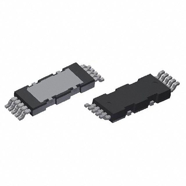
PG-HDSOP-10-1
Key performance parameters
Parameter
Value
Unit
VRRM
650
V
QC (VR = 400 V)
9.6
nC
EC (VR = 400 V)
1.6
µJ
IF (TC ≤
6
A
1.25
V
0 °C, D = 1)
VF (IF = 6 A, Tj = 25 °C)
Cathode
Pin 6-10
Table 2
Package information
Pin 1-2: n.c.
Pin 3-5: Anode
Type / ordering Code
Package
Marking
IDDD06G65C6
PG-HDSOP-10-1
D0665C6
Pin 3-5
Pin 6-10: Cathode
Features
Best in class forward voltage (1.25 V)
Best in class figure of merit (Qc x VF)
High dv/dt ruggedness (150 V/ns)
Benefits
System efficiency improvement
System cost and size savings due to the reduced cooling requirements
Enabling higher frequency and increased power density
Potential Applications
Power factor correction in SMPS
Solar inverter
Uninterruptible power supply
Product Validation
Qualified for industrial applications according to the relevant tests of JEDEC (J-STD20 and JESD22)
Final Datasheet
Please read the Important Notice and Warnings at the end of this document
Rev. 2.0, 2018-02-06
�6th Generation CoolSiCTM
IDDD06G65C6
Table of Content
1
Maximum ratings ............................................................................................................................... 3
2
Thermal characteristics ..................................................................................................................... 3
3
3.1
3.2
Electrical characteristics .................................................................................................................... 4
Static characteristics ............................................................................................................................... 4
AC characteristics .................................................................................................................................... 4
4
Diagrams ............................................................................................................................................ 5
5
Simplified forward characteristic ....................................................................................................... 7
6
Package outlines ................................................................................................................................ 8
Final Datasheet
2
Rev. 2.0 , 2018-02-06
�6th Generation CoolSiCTM
IDDD06G65C6
1
Table 3
Maximum ratings
Maximum ratings
Parameter
Symbol
Continuous forward current
IF
Values
Unit
Note/Test condition
Min.
Typ.
Max.
–
–
6
TC ≤ 150 °C, D = 1
–
–
10
TC ≤ 125 °C, D = 1
–
–
18
TC ≤
–
–
26
–
–
38
TC = 25 °C, tp = 10 ms
–
–
30
TC = 150 °C, tp = 10 ms
–
–
410
TC = 25 °C, tp = 10 µs
–
–
7.2
–
–
4.6
°C, D = 1
Surge-repetitive forward current,
sine halfwave1
IF,RM
Surge non-repetitive forward
current, sine halfwave
IF,SM
Non-repetitive peak forward
current
IF,max
i²t value
∫ i²dt
Repetitive peak reverse voltage
VRRM
–
–
650
V
TC = 25 °C
Diode dv/dt ruggedness
dv/dt
–
–
150
V/ns
VR = 0..480 V
Power dissipation
Ptot
–
–
73
W
TC = 25°C, RthJC,max
Operating and storage
temperature
Tj
Tstg
-55
–
175
°C
–
Unit
Note/Test condition
2
Table 4
A
A²s
TC = 25 °C, tp = 10 ms
TC = 150 °C, tp = 10 ms
Thermal characteristics
Thermal characteristics
Parameter
Symbol
Thermal resistance, junctioncase
Thermal resistance, junctionambient
Values
Min.
Typ.
Max.
RthJC
–
1.2
2.0
–
RthJA
–
–
62
Device on PCB, minimal
footprint
K/W
Thermal resistance, junctionambient for SMD version
Soldering temperature
1
TC = 25 °C, tp = 10 ms
RthJA
–
35
45
Tsold
–
–
260
°C
Device on 40*40*1.5 mm
epoxy PCB FR4 (one layer,
70 µm thickness) with 6
cm2 copper for cathode
connection and cooling,
PCB vertically placed
without air stream cooling
Allowed only reflow
soldering
The surge-repetitive forward current test was performed with 1000 pulses (half-wave rectified sine with the 10 ms period).
Final Datasheet
3
Rev. 2.0 , 2018-02-06
�6th Generation CoolSiCTM
IDDD06G65C6
3
Electrical characteristics
Static characteristics
3.1
Table 5
Static characteristics
Parameter
Symbol
DC blocking voltage
VDC
Diode forward voltage
VF
Reverse current
Note/Test condition
Typ.
Max.
650
–
–
–
1.25
1.35
–
1.5
–
IF = 6 A, Tj = 150 °C
–
0.6
20
VR = 420 V, Tj = 25 °C
–
20
–
–
46
–
Tj = 25 °C
V
µA
IF = 6 A, Tj = 25 °C
VR = 420 V, Tj = 125 °C
VR = 420 V, Tj = 150 °C
AC characteristics
Parameter
Symbol
Total capacitive charge
Qc
Total capacitance
Final Datasheet
Unit
Min.
AC characteristics
3.2
Table 6
IR
Values
C
Values
Min.
Typ.
Max.
–
9.6
–
–
302
–
–
18
–
–
17
–
4
Unit
Note/Test Condition
nC
VR = 400 V, Tj = 150 °C,
di/dt = 200 A/µs, IF ≤ IF,MAX
VR = 1 V, f = 1 MHz,
Tj = 25 °C
pF
VR = 300 V, f = 1 MHz,
Tj = 25 °C
VR = 600 V, f = 1 MHz,
Tj = 25 °C
Rev. 2.0 , 2018-02-06
�6th Generation CoolSiCTM
IDDD06G65C6
Diagrams
4
IF = f(TC); RthJC,max ; Tj ≤ 175 °C; parameter: D = tP/T
Ptot = f(TC)
Figure 1
Power dissipation
Figure 2
IF = f(VF); tp = 10 µs; parameter: Tj
Figure 3
Typ. forward characteristics
Final Datasheet
Max. forward current
IF = f(VF); tp = 10 µs; parameter: Tj
Figure 4
5
Typ. forward characteristics
in surge current
Rev. 2.0 , 2018-02-06
�6th Generation CoolSiCTM
IDDD06G65C6
QC = f(diF/dt); Tj = 150 °C; VR = 400 V; IF ≤ IF,max
Figure 5
Typ. cap. charge vs. current slope
IR = f(VR); parameter: Tj
Figure 6
Zth,jc = f(tP); parameter: D = tP/T
Figure 7
Max. transient thermal
impedance
Final Datasheet
Typ. reverse current vs. reverse voltage
C = f(VR); Tj = 25 °C; f = 1 MHz
Figure 8
6
Typ. capacitance vs. reverse voltage
Rev. 2.0 , 2018-02-06
�6th Generation CoolSiCTM
IDDD06G65C6
EC = f(VR)
Figure 9
Typ. capacitance stored energy
Simplified forward characteristic
5
VF VTH RDIFF I F
Treshold voltage (VTH):
VTH T j 0.001 T j 0.766 V
Differential resistance (RDIFF):
2
RDIFF T j A T j B T j C
A 2.07 10 -6
DIFF
B 1.50 10 -4
TH
C 7.94 10-2
Tj [°C]; -55 °C ≤ Tj ≤ 175 °C; IF ≤ 6 A
VF = f(IF)
Figure 10
Equivalent forward current curve
Final Datasheet
Figure 11
7
Mathematical Equation
Rev. 2.0 , 2018-02-06
�6th Generation CoolSiCTM
IDDD06G65C6
6
Package outlines
Figure 12
Outlines of the package PG-HDSOP-10-1, dimensions in milimeters
Final Datasheet
8
Rev. 2.0 , 2018-02-06
�6th�Generation�CoolSiCª
IDDD06G65C6
Revision�History
IDDD06G65C6
Revision:�2018-02-26,�Rev.�2.0
Previous Revision
Revision
Date
Subjects (major changes since last revision)
2.0
2018-02-26
Release of final version
Trademarks�of�Infineon�Technologies�AG
AURIX™,�C166™,�CanPAK™,�CIPOS™,�CoolGaN™,�CoolMOS™,�CoolSET™,�CoolSiC™,�CORECONTROL™,�CROSSAVE™,�DAVE™,�DI-POL™,�DrBlade™,
EasyPIM™,�EconoBRIDGE™,�EconoDUAL™,�EconoPACK™,�EconoPIM™,�EiceDRIVER™,�eupec™,�FCOS™,�HITFET™,�HybridPACK™,�Infineon™,
ISOFACE™,�IsoPACK™,�i-Wafer™,�MIPAQ™,�ModSTACK™,�my-d™,�NovalithIC™,�OmniTune™,�OPTIGA™,�OptiMOS™,�ORIGA™,�POWERCODE™,
PRIMARION™,�PrimePACK™,�PrimeSTACK™,�PROFET™,�PRO-SIL™,�RASIC™,�REAL3™,�ReverSave™,�SatRIC™,�SIEGET™,�SIPMOS™,�SmartLEWIS™,
SOLID�FLASH™,�SPOC™,�TEMPFET™,�thinQ�™,�TRENCHSTOP™,�TriCore™.
Trademarks�updated�August�2015
Other�Trademarks
All�referenced�product�or�service�names�and�trademarks�are�the�property�of�their�respective�owners.
We�Listen�to�Your�Comments
Any�information�within�this�document�that�you�feel�is�wrong,�unclear�or�missing�at�all?�Your�feedback�will�help�us�to�continuously
improve�the�quality�of�this�document.�Please�send�your�proposal�(including�a�reference�to�this�document)�to:
erratum@infineon.com
Published�by
Infineon�Technologies�AG
81726�München,�Germany
©�2018�Infineon�Technologies�AG
All�Rights�Reserved.
Legal�Disclaimer
The�information�given�in�this�document�shall�in�no�event�be�regarded�as�a�guarantee�of�conditions�or�characteristics�
(“Beschaffenheitsgarantie”)�.
With�respect�to�any�examples,�hints�or�any�typical�values�stated�herein�and/or�any�information�regarding�the�application�of�the
product,�Infineon�Technologies�hereby�disclaims�any�and�all�warranties�and�liabilities�of�any�kind,�including�without�limitation
warranties�of�non-infringement�of�intellectual�property�rights�of�any�third�party.
In�addition,�any�information�given�in�this�document�is�subject�to�customer’s�compliance�with�its�obligations�stated�in�this
document�and�any�applicable�legal�requirements,�norms�and�standards�concerning�customer’s�products�and�any�use�of�the
product�of�Infineon�Technologies�in�customer’s�applications.
The�data�contained�in�this�document�is�exclusively�intended�for�technically�trained�staff.�It�is�the�responsibility�of�customer’s
technical�departments�to�evaluate�the�suitability�of�the�product�for�the�intended�application�and�the�completeness�of�the�product
information�given�in�this�document�with�respect�to�such�application.
Information
For�further�information�on�technology,�delivery�terms�and�conditions�and�prices�please�contact�your�nearest�Infineon
Technologies�Office�(www.infineon.com).
Warnings
Due�to�technical�requirements,�components�may�contain�dangerous�substances.�For�information�on�the�types�in�question,
please�contact�the�nearest�Infineon�Technologies�Office.
The�Infineon�Technologies�component�described�in�this�Data�Sheet�may�be�used�in�life-support�devices�or�systems�and/or
automotive,�aviation�and�aerospace�applications�or�systems�only�with�the�express�written�approval�of�Infineon�Technologies,�if�a
failure�of�such�components�can�reasonably�be�expected�to�cause�the�failure�of�that�life-support,�automotive,�aviation�and
aerospace�device�or�system�or�to�affect�the�safety�or�effectiveness�of�that�device�or�system.�Life�support�devices�or�systems�are
intended�to�be�implanted�in�the�human�body�or�to�support�and/or�maintain�and�sustain�and/or�protect�human�life.�If�they�fail,�it�is
reasonable�to�assume�that�the�health�of�the�user�or�other�persons�may�be�endangered.
9
Rev.�2.0,��2018-02-26
�


 工商网监
湘ICP备2023018690号
工商网监
湘ICP备2023018690号
