PD - 95503B
IRF5804PbF
HEXFET® Power MOSFET
l
l
l
l
l
l
l
Ultra Low On-Resistance
P-Channel MOSFET
Surface Mount
Available in Tape & Reel
Low Gate Charge
Lead-Free
Halogen-Free
Description
These P-channel HEXFET® Power MOSFETs from
International Rectifier utilize advanced processing
techniques to achieve the extremely low on-resistance
per silicon area. This benefit provides the designer
with an extremely efficient device for use in battery and
load management applications.
VDSS
RDS(on) max (mW)
ID
-40V
198@VGS = -10V
334@VGS = -4.5V
-2.5A
-2.0A
A
D
D
1
6
D
2
5
D
G
3
4
S
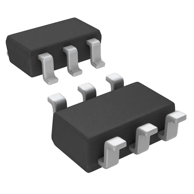
TSOP-6
Top View
The TSOP-6 package with its customized leadframe
produces a HEXFET® power MOSFET with RDS(on)
60% less than a similar size SOT-23. This package is
ideal for applications where printed circuit board space
is at a premium. It's unique thermal design and R DS(on)
reduction enables a current-handling increase of nearly
300% compared to the SOT-23.
Absolute Maximum Ratings
Parameter
VDS
ID @ TA = 25°C
ID @ TA= 70°C
IDM
PD @TA = 25°C
PD @TA = 70°C
VGS
TJ, TSTG
Drain- Source Voltage
Continuous Drain Current, VGS @ -10V
Continuous Drain Current, VGS @ -10V
Pulsed Drain Current
Power Dissipation
Power Dissipation
Linear Derating Factor
Gate-to-Source Voltage
Junction and Storage Temperature Range
Max.
Units
-40
-2.5
-2.0
-10
2.0
1.3
0.016
± 20
-55 to + 150
V
mW/°C
V
°C
Max.
Units
62.5
°C/W
A
W
Thermal Resistance
Parameter
RθJA
www.irf.com
Maximum Junction-to-Ambient
1
04/20/10
�IRF5804PbF
Electrical Characteristics @ TJ = 25°C (unless otherwise specified)
∆V(BR)DSS/∆TJ
Parameter
Drain-to-Source Breakdown Voltage
Breakdown Voltage Temp. Coefficient
RDS(on)
Static Drain-to-Source On-Resistance
VGS(th)
gfs
Gate Threshold Voltage
Forward Transconductance
IDSS
Drain-to-Source Leakage Current
V(BR)DSS
IGSS
Qg
Qgs
Qgd
td(on)
tr
td(off)
tf
Ciss
Coss
Crss
Gate-to-Source Forward Leakage
Gate-to-Source Reverse Leakage
Total Gate Charge
Gate-to-Source Charge
Gate-to-Drain ("Miller") Charge
Turn-On Delay Time
Rise Time
Turn-Off Delay Time
Fall Time
Input Capacitance
Output Capacitance
Reverse Transfer Capacitance
Min.
-40
–––
–––
–––
-1.0
2.5
–––
–––
–––
–––
–––
–––
–––
–––
–––
–––
–––
–––
–––
–––
Typ.
–––
0.03
–––
–––
–––
–––
–––
–––
–––
–––
5.7
2.8
2.1
19
430
100
64
680
60
44
Max. Units
Conditions
–––
V
VGS = 0V, ID = -250µA
––– V/°C Reference to 25°C, ID = -1mA
198
VGS = -10V, ID = -2.5
mΩ
334
VGS = -4.5V, ID = -2.0A
-3.0
V
VDS = VGS, ID = -250µA
–––
S
VDS = -10V, ID = -2.5A
-10
VDS = -32V, VGS = 0V
µA
-25
VDS = -32V, VGS = 0V, TJ = 70°C
-100
VGS = -20V
nA
100
VGS = 20V
8.5
ID = -2.5A
4.2
nC
VDS = -20V
3.2
VGS = -10V
–––
VDD = -20V
–––
ID = -1.0A
ns
–––
RG = 6.0Ω
–––
VGS = -10V
–––
VGS = 0V
–––
pF
VDS = -25V
–––
ƒ = 1kHz
Source-Drain Ratings and Characteristics
IS
ISM
VSD
trr
Qrr
Parameter
Continuous Source Current
(Body Diode)
Pulsed Source Current
(Body Diode)
Diode Forward Voltage
Reverse Recovery Time
Reverse Recovery Charge
Min. Typ. Max. Units
-2.5
-10
–––
–––
–––
–––
24
32
-1.2
36
49
A
V
ns
nC
Conditions
MOSFET symbol
showing the
G
integral reverse
p-n junction diode.
TJ = 25°C, IS = -2.0A, VGS = 0V
TJ = 25°C, IF = -2.0A
di/dt = -100A/µs
D
S
Notes:
Repetitive rating; pulse width limited by
max. junction temperature.
Surface mounted on 1 in square Cu board
Pulse width ≤ 400µs; duty cycle ≤ 2%.
2
www.irf.com
�IRF5804PbF
100
100
VGS
-10V
-7.0V
-5.0V
-4.5V
-4.0V
-3.7V
-3.5V
BOTTOM -3.0V
VGS
-10V
-7.0V
-5.0V
-4.5V
-4.0V
-3.7V
-3.5V
BOTTOM -3.0V
TOP
10
-I D, Drain-to-Source Current (A)
-I D , Drain-to-Source Current (A)
TOP
1
-3.0V
0.1
20µs PULSE WIDTH
Tj = 25°C
10
1
-3.0V
20µs PULSE WIDTH
Tj = 150°C
0.1
0.01
0.1
1
10
100
0.1
-V DS , Drain-to-Source Voltage (V)
Fig 1. Typical Output Characteristics
2.0
RDS(on) , Drain-to-Source On Resistance
(Normalized)
-I D, Drain-to-Source Current (Α)
T J = 150°C
1.00
TJ = 25°C
VDS = -25V
20µs PULSE WIDTH
3.0
3.5
4.0
4.5
-V GS, Gate-to-Source Voltage (V)
Fig 3. Typical Transfer Characteristics
www.irf.com
10
100
Fig 2. Typical Output Characteristics
10.00
0.10
1
-V DS , Drain-to-Source Voltage (V)
5.0
ID = -2.5A
1.5
1.0
0.5
0.0
-60 -40 -20
VGS = -10V
0
20
40
60
80 100 120 140 160
TJ , Junction Temperature ( °C)
Fig 4. Normalized On-Resistance
Vs. Temperature
3
�IRF5804PbF
VGS = 0V,
f = 1 MHZ
Ciss = Cgs + Cgd , Cds SHORTED
Crss = Cgd
C, Capacitance(pF)
Coss = Cds + Cgd
1000
Ciss
100
Coss
Crss
12
-VGS , Gate-to-Source Voltage (V)
10000
10
1
10
8
6
4
2
0
2
6
8
10
Fig 6. Typical Gate Charge Vs.
Gate-to-Source Voltage
Fig 5. Typical Capacitance Vs.
Drain-to-Source Voltage
10
100
-I D, Drain-to-Source Current (A)
-ISD , Reverse Drain Current (A)
4
QG , Total Gate Charge (nC)
- -V DS , Drain-to-Source Voltage (V)
TJ = 150 ° C
1
TJ = 25 ° C
0.1
0.4
V GS = 0 V
0.6
0.7
0.9
1.1
1.2
-VSD ,Source-to-Drain Voltage (V)
4
VDS = 32V
VDS = 20V
10
0
100
ID = 2.5A
Fig 7. Typical Source-Drain Diode
Forward Voltage
OPERATION IN THIS AREA
LIMITED BY R DS(on)
10
100µsec
1
1msec
0.1
1.4
Tc = 25°C
Tj = 150°C
Single Pulse
1
10msec
10
100
1000
-VDS , Drain-toSource Voltage (V)
Fig 8. Maximum Safe Operating Area
www.irf.com
�IRF5804PbF
2.5
VDS
VGS
-ID , Drain Current (A)
2.0
RD
D.U.T.
RG
-
+
1.5
VDD
VGS
Pulse Width ≤ 1 µs
Duty Factor ≤ 0.1 %
1.0
Fig 10a. Switching Time Test Circuit
0.5
td(on)
tr
t d(off)
tf
VGS
0.0
25
50
75
100
125
TC , Case Temperature ( °C)
10%
150
90%
Fig 9. Maximum Drain Current Vs.
Case Temperature
VDS
Fig 10b. Switching Time Waveforms
Thermal Response (Z thJA )
100
D = 0.50
0.20
10
0.10
0.05
0.02
0.01
1
P DM
SINGLE PULSE
(THERMAL RESPONSE)
t1
t2
0.1
0.00001
Notes:
1. Duty factor D = t 1 / t 2
2. Peak T J = P DM x Z thJA + TA
0.0001
0.001
0.01
0.1
1
10
t1 , Rectangular Pulse Duration (sec)
Fig 11. Maximum Effective Transient Thermal Impedance, Junction-to-Ambient
www.irf.com
5
�0.40
0.40
R DS (on) , Drain-to-Source On Resistance (Ω)
RDS(on) , Drain-to -Source On Resistance (Ω)
IRF5804PbF
0.35
0.30
0.25
0.20
ID = -2.5A
0.15
0.10
0.35
0.30
VGS = -4.5V
0.25
0.20
0.15
VGS = -10V
0.10
4.0
5.0
6.0
7.0
8.0
9.0
10.0
1
2
3
-V GS, Gate -to -Source Voltage (V)
Fig 12. Typical On-Resistance Vs.
Gate Voltage
4
5
6
7
8
9
-I D , Drain Current (A)
Fig 13. Typical On-Resistance Vs.
Drain Current
Current Regulator
Same Type as D.U.T.
50KΩ
QG
QGS
.2µF
.3µF
QGD
D.U.T.
+VDS
VGS
VG
-3mA
Charge
Fig 14a. Basic Gate Charge Waveform
6
12V
IG
ID
Current Sampling Resistors
Fig 14b. Gate Charge Test Circuit
www.irf.com
10
�IRF5804PbF
70
60
50
2.5
ID = -250µA
Power (W)
VGS(th) Gate threshold Voltage (V)
3.0
2.0
40
30
20
10
1.5
0
-75
-50
-25
0
25
50
75
100
125
T J , Temperature ( °C )
Fig 15. Typical Threshold Voltage Vs.
Junction Temperature
www.irf.com
150
1.00
10.00
100.00
1000.00
Time (sec)
Fig 16. Typical Power Vs. Time
7
�IRF5804PbF
TSOP-6 Package Outline
TSOP-6 Part Marking Information
5
$
(
�<
5
$
'
1
(
/
$
�&
)
�2
,7
,*
�'
7
6
$
�/
<
�%
'
(
'
(
&
(
5
�3
,)
��
�
��
�
��
�
:
: $ % & '
..
5(
2( � � � �
:: � � � �
�
�
�
�
�
�
�
�
7
2
/
�
�
�
�
�
�
�
�
5
2
7
$
,&
'
�,1
(
,5
�:
8
&
3
2
7
(
'
2
&
�
�
�
�
�
�
�
�
; < =
�
(
&
1
(
5
(
)
(
�5
(
'
2
�&
5
(
%
0
8
�1
7
5
$
3
� � �
� � �
�
�
�
�
� � � � � � � � � �
�
�
�
�
<
.
(
(
�:
�
:
�
�
�
�
�
�
�
�
5
$
(
�<
�
<
5
$
(
<
(
'
2
�&
(
7
$
'
5
(
%
0
8
�1
7
5
$
3
: $ % & '
..
5(
2( � � � �
:: � � � �
�
�
�
�
; < =
� � �
� � �
�
�
�
�
$ % & ' ( ) * + - .
�
�
�
�
<
�
�
�
�
�
�
�
�
�
�
�
�
�
�
�
�
�
�
�
�
�
�
�
�
�
�
�
�
)
�,5
�
1
�
�
�
�
�
�
�
�
)
�,5
�
0
5
$
(
<
�
�
�
�
)
�,5
�
/
5
(
7
7
(
�/
�$
<
�%
'
(
'
(
&
(
5
�3
,)
��
�
��
�
�
��
�
:
�
�
�
�
)
�,5
�
.
�
�
�
�
)
�,5
-�
�
�
�
�
)
�,5
�
'
�
�
�
�
)
�,5
,�
�
�
�
�
)
�,5
�
&
�
�
�
�
)
�,5
�
)
�
�
�
�
)
�,5
�
%
LUH
�Z
X
&
V�
WH
D
LF
G
LQ
��
UH
H
�K
Q
Z
R
VK
V�
�D
U�
H
E
P
X
�Q
UW
D
�S
H
�WK
Z
OR
H
�E
H
Q
�OL
�$
�
�
�
�
)
�,5
�
(
9
'
�
�
�
,�
�6
�
$
H
UH
�)
G
D
H
/
V�
WH
D
LF
G
LQ
��
UH
H
�K
Q
Z
R
VK
V�
�D
N�
H
H
�Z
UN
R
�Z
H
K
�W
YH
R
E
�D
H
Q
�OL
�$
www.irf.com
8
�
V�
WH
R
1
Note: For the most current drawing please refer to IR website at: http://www.irf.com/package/
�IRF5804PbF
TSOP-6 Tape & Reel Information
Data and specifications subject to change without notice.
This product has been designed and qualified for the Consumer market.
Qualification Standards can be found on IR’s Web site.
IR WORLD HEADQUARTERS: 233 Kansas St., El Segundo, California 90245, USA Tel: (310) 252-7105
TAC Fax: (310) 252-7903
Visit us at www.irf.com for sales contact information.04/2010
www.irf.com
9
�


 工商网监
湘ICP备2023018690号
工商网监
湘ICP备2023018690号
