PD - 95137A
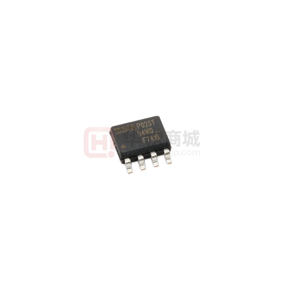
IRF7416PbF
l
l
l
l
l
l
l
l
HEXFET® Power MOSFET
Generation V Technology
Ultra Low On-Resistance
P-Channel Mosfet
Surface Mount
Available in Tape & Reel
Dynamic dv/dt Rating
Fast Switching
Lead-Free
A
D
1
8
S
2
7
D
S
3
6
D
G
4
5
D
S
VDSS = -30V
RDS(on) = 0.02Ω
Top View
Description
Fifth Generation HEXFETs from International Rectifier
utilize advanced processing techniques to achieve
extremely low on-resistance per silicon area. This benefit,
combined with the fast switching speed and ruggedized
device design that HEXFET Power MOSFETs are well
known for, provides the designer with an extremely efficient
and reliable device for use in a wide variety of applications.
The SO-8 has been modified through a customized
leadframe for enhanced thermal characteristics and
multiple-die capability making it ideal in a variety of power
applications. With these improvements, multiple devices
can be used in an application with dramatically reduced
board space. The package is designed for vapor phase,
infra red, or wave soldering techniques. Power dissipation
of greater than 0.8W is possible in a typical PCB mount
application.
SO-8
Absolute Maximum Ratings
Parameter
Max.
ID @ TA = 25°C
Continuous Drain Current, VGS @ -10V
-10
ID @ TA = 70°C
Continuous Drain Current, VGS @ -10V
-7.1
IDM
Pulsed Drain Current
PD @TA = 25°C
VGS
Power Dissipation
Linear Derating Factor
Gate-to-Source Voltage
EAS
Single Pulse Avalanche Energy
dv/dt
Peak Diode Recovery dv/dt
TJ
Operating Junction and
TSTG
Storage Temperature Range
c
Units
A
-45
e
d
2.5
0.02
± 20
W
W/°C
V
370
mJ
-5.0
V/ns
-55 to + 150
°C
Max.
Units
50
°C/W
Thermal Resistance
Parameter
RθJA
www.irf.com
Junction-to-Ambient
g
1
06/29/11
�IRF7416PbF
Static Electrical Characteristics @ TJ = 25°C (unless otherwise specified)
Parameter
Min. Typ. Max. Units
V(BR)DSS
Drain-to-Source Breakdown Voltage
ΔV(BR)DSS/ΔTJ Breakdown Voltage Temp. Coefficient
RDS(on)
Static Drain-to-Source On-Resistance
VGS(th)
gfs
IDSS
Gate Threshold Voltage
Forward Transconductance
Drain-to-Source Leakage Current
IGSS
Gate-to-Source Forward Leakage
Gate-to-Source Reverse Leakage
Conditions
-30
––– –––
V VGS = 0V, ID = -250μA
––– -0.024 ––– V/°C Reference to 25°C, ID = -1mA
VGS = -10V, ID = -5.6A
––– ––– 0.020
Ω
VGS = -4.5V, ID = -2.8A
––– ––– 0.035
-1.0 ––– -2.04
V VDS = VGS, ID = -250μA
5.6
––– –––
S VDS = -10V, ID = -2.8A
VDS = -24V, VGS = 0V
––– ––– -1.0
μA
VDS = -24V, VGS = 0V, TJ = 125°C
––– –––
-25
VGS = -20V
––– ––– -100
nA
––– ––– 100
VGS = 20V
f
f
Dynamic Electrical Characteristics @ TJ = 25°C (unless otherwise specified)
Parameter
Min. Typ. Max. Units
Conditions
Qg
Qgs
Qgd
td(on)
tr
td(off)
tf
Ciss
Coss
Crss
Total Gate Charge
Gate-to-Source Charge
Gate-to-Drain ("Miller") Charge
Turn-On Delay Time
Rise Time
Turn-Off Delay Time
Fall Time
Input Capacitance
Output Capacitance
Reverse Transfer Capacitance
–––
–––
–––
–––
–––
–––
–––
–––
–––
–––
61
8.0
22
18
49
59
60
1700
890
410
92
12
32
–––
–––
–––
–––
–––
–––
–––
nC
ns
pF
ID = -5.6A
VDS = -24V
VGS = -10V, See Fig. 6 & 9
VDD = -15V
ID = -5.6A
RG = 6.2Ω
RD = 2.7Ω, See Fig. 10
VGS = 0V
VDS = -25V
ƒ = 1.0MHz, See Fig. 5
f�
f
Diode Characteristics
Parameter
IS
Continuous Source Current
ISM
VSD
trr
Qrr
(Body Diode)
Pulsed Source Current
(Body Diode)
Diode Forward Voltage
Reverse Recovery Time
Reverse Recovery Charge
�c
Min. Typ. Max. Units
–––
–––
-3.1
A
–––
–––
-45
–––
–––
–––
–––
56
99
-1.0
85
150
Conditions
MOSFET symbol
V
ns
nC
showing the
integral reverse
D
G
S
p-n junction diode.
TJ = 25°C, IS = -5.6A, VGS = 0V
TJ = 25°C,IF = -5.6A
di/dt = 100A/μs
e
e
Notes:
Repetitive rating; pulse width limited by
ISD ≤ -5.6A, di/dt ≤ 100A/µs, VDD ≤ V(BR)DSS,
Starting TJ = 25°C, L = 25mH
Pulse width ≤ 300µs; duty cycle ≤ 2%.
max. junction temperature. ( See fig. 11 )
RG = 25Ω, IAS = -5.6A. (See Figure 12)
2
T J ≤ 150°C
Surface mounted on FR-4 board, t ≤ 10sec.
www.irf.com
�IRF7416PbF
100
100
VGS
- 15V
- 10V
- 7.0V
- 5.5V
- 4.5V
- 4.0V
- 3.5V
BOTTOM - 3.0V
-I D , Drain-to-Source Current (A)
-I D , Drain-to-Source Current (A)
VGS
- 15V
- 10V
- 7.0V
- 5.5V
- 4.5V
- 4.0V
- 3.5V
BOTTOM - 3.0V
TOP
TOP
10
-3.0V
20μs PULSE WIDTH
TJ = 25°C
A
1
0.1
1
10
-3.0V
20μs PULSE WIDTH
TJ = 150°C
A
1
0.1
10
1
Fig 2. Typical Output Characteristics
Fig 1. Typical Output Characteristics
2.0
R DS(on) , Drain-to-Source On Resistance
(Normalized)
-ID , Drain-to-Source Current (A)
100
TJ = 25°C
TJ = 150°C
10
VDS = -10V
20μs PULSE WIDTH
1
3.0
3.5
4.0
4.5
5.0
-VGS , Gate-to-Source Voltage (V)
Fig 3. Typical Transfer Characteristics
www.irf.com
10
-VDS , Drain-to-Source Voltage (V)
-VDS , Drain-to-Source Voltage (V)
5.5
A
I D = -5.6A
1.5
1.0
0.5
VGS = -10V
0.0
-60
-40
-20
0
20
40
60
80
A
100 120 140 160
TJ , Junction Temperature (°C)
Fig 4. Normalized On-Resistance
Vs. Temperature
3
�IRF7416PbF
20
V GS = 0V,
f = 1MHz
C iss = Cgs + C gd , Cds SHORTED
C rss = C gd
C oss = C ds + C gd
-VGS , Gate-to-Source Voltage (V)
C, Capacitance (pF)
4000
3000
Ciss
Coss
2000
1000
Crss
0
1
10
100
I D = -5.6A
VDS = -24V
VDS = -15V
16
12
A
8
4
FOR TEST CIRCUIT
SEE FIGURE 9
0
0
VDS , Drain-to-Source Voltage (V)
60
80
100
-IID , Drain Current (A)
OPERATION IN THIS AREA LIMITED
BY RDS(on)
TJ = 150°C
10
TJ = 25°C
VGS = 0V
1
0.4
0.6
0.8
1.0
-VSD , Source-to-Drain Voltage (V)
Fig 7. Typical Source-Drain Diode
Forward Voltage
A
1.2
100us
10
1ms
10ms
TA = 25 °C
TJ = 150 ° C
Single Pulse
1
0.1
1
10
A
100
Fig 6. Typical Gate Charge Vs.
Gate-to-Source Voltage
100
-ISD , Reverse Drain Current (A)
40
Q G , Total Gate Charge (nC)
Fig 5. Typical Capacitance Vs.
Drain-to-Source Voltage
4
20
100
-VDS , Drain-to-Source Voltage (V)
Fig 8. Maximum Safe Operating Area
www.irf.com
�IRF7416PbF
QG
-10V
QGS
RD
VDS
V GS
D.U.T.
RG
QGD
VG
-
+
VDD
-10V
Pulse Width ≤ 1 µs
Duty Factor ≤ 0.1 %
Charge
Fig 9a. Basic Gate Charge Waveform
Fig 10a. Switching Time Test Circuit
Current Regulator
Same Type as D.U.T.
td(on)
50KΩ
12V
tr
t d(off)
tf
VGS
.2μF
.3μF
10%
+VDS
D.U.T.
VGS
90%
-3mA
VDS
IG
ID
Current Sampling Resistors
Fig 9b. Gate Charge Test Circuit
Fig 10b. Switching Time Waveforms
Thermal Response (Z thJA )
100
D = 0.50
10
0.20
0.10
0.05
PDM
0.02
1
0.01
t1
t2
SINGLE PULSE
(THERMAL RESPONSE)
0.1
0.0001
0.001
Notes:
1. Duty factor D = t 1 / t 2
2. Peak TJ = P DM x Z thJA + TA
0.01
0.1
1
10
100
t1 , Rectangular Pulse Duration (sec)
Fig 11. Maximum Effective Transient Thermal Impedance, Junction-to-Ambient
www.irf.com
5
�IRF7416PbF
D.U.T
RG
IAS
-20V
tp
VDD
A
DRIVER
0.01Ω
15V
Fig 12a. Unclamped Inductive Test Circuit
I AS
EAS , Single Pulse Avalanche Energy (mJ)
1000
L
VDS
ID
-2.5A
-4.5A
BOTTOM -5.6A
TOP
800
600
400
200
0
25
50
75
100
125
150
Starting TJ , Junction Temperature (o C)
Fig 12c. Maximum Avalanche Energy
Vs. Drain Current
tp
V(BR)DSS
Fig 12b. Unclamped Inductive Waveforms
6
www.irf.com
�IRF7416PbF
Peak Diode Recovery dv/dt Test Circuit
+
D.U.T
Circuit Layout Considerations
• Low Stray Inductance
• Ground Plane
• Low Leakage Inductance
Current Transformer
+
-
-
+
**
RG
• dv/dt controlled by RG
• ISD controlled by Duty Factor "D"
• D.U.T. - Device Under Test
VGS*
+
-
*
VDD
*
Reverse Polarity for P-Channel
** Use P-Channel Driver for P-Channel Measurements
Driver Gate Drive
Period
P.W.
D=
P.W.
Period
[VGS=10V ] ***
D.U.T. ISD Waveform
Reverse
Recovery
Current
Body Diode Forward
Current
di/dt
D.U.T. VDS Waveform
Diode Recovery
dv/dt
Re-Applied
Voltage
Body Diode
[ VDD]
Forward Drop
Inductor Curent
Ripple ≤ 5%
[ ISD]
*** VGS = 5.0V for Logic Level and 3V Drive Devices
Fig 13. For P-Channel HEXFETS
www.irf.com
7
�IRF7416PbF
SO-8 Package Outline
Dimensions are shown in millimeters (inches)
D
5
A
8
6
7
6
5
H
1
2
3
0.25 [.010]
4
A
MAX
MIN
.0532
.0688
1.35
1.75
A1 .0040
e
e1
8X b
0.25 [.010]
MAX
0.25
.0098
0.10
b
.013
.020
0.33
0.51
c
.0075
.0098
0.19
0.25
D
.189
.1968
4.80
5.00
E
.1497
.1574
3.80
4.00
e
.050 BASIC
1.27 BASIC
.025 BASIC
0.635 BASIC
e1
6X
MILLIMETERS
MIN
A
E
INCHES
DIM
B
H
.2284
.2440
5.80
6.20
K
.0099
.0196
0.25
0.50
L
.016
.050
0.40
1.27
y
0°
8°
0°
8°
K x 45°
A
C
y
0.10 [.004]
A1
8X L
8X c
7
C A B
F OOTPRINT
NOT ES :
1. DIMENS IONING & TOLERANCING PER ASME Y14.5M-1994.
8X 0.72 [.028]
2. CONT ROLLING DIMENS ION: MILLIMET ER
3. DIMENS IONS ARE SHOWN IN MILLIMETERS [INCHES].
4. OUTLINE CONFORMS TO JEDEC OUTLINE MS -012AA.
5 DIMENS ION DOES NOT INCLUDE MOLD PROT RUSIONS .
MOLD PROTRUS IONS NOT TO EXCEED 0.15 [.006].
6 DIMENS ION DOES NOT INCLUDE MOLD PROT RUSIONS .
MOLD PROTRUS IONS NOT TO EXCEED 0.25 [.010].
6.46 [.255]
7 DIMENS ION IS T HE LENGT H OF LEAD FOR SOLDERING TO
A S UBST RAT E.
3X 1.27 [.050]
8X 1.78 [.070]
SO-8 Part Marking
EXAMPLE: T HIS IS AN IRF7101 (MOSFET )
INT ERNAT IONAL
RECT IFIER
LOGO
XXXX
F7101
DAT E CODE (YWW)
P = DES IGNAT ES LEAD-FREE
PRODUCT (OPT IONAL)
Y = LAS T DIGIT OF T HE YEAR
WW = WEEK
A = AS S EMBLY S IT E CODE
LOT CODE
PART NUMBER
8
www.irf.com
�IRF7416PbF
SO-8 Tape and Reel
Dimensions are shown in millimeters (inches)
TERMINAL NUMBER 1
12.3 ( .484 )
11.7 ( .461 )
8.1 ( .318 )
7.9 ( .312 )
FEED DIRECTION
NOTES:
1. CONTROLLING DIMENSION : MILLIMETER.
2. ALL DIMENSIONS ARE SHOWN IN MILLIMETERS(INCHES).
3. OUTLINE CONFORMS TO EIA-481 & EIA-541.
330.00
(12.992)
MAX.
14.40 ( .566 )
12.40 ( .488 )
NOTES :
1. CONTROLLING DIMENSION : MILLIMETER.
2. OUTLINE CONFORMS TO EIA-481 & EIA-541.
Data and specifications subject to change without notice.
This product has been designed and qualified for the Consumer market.
Qualifications Standards can be found on IR’s Web site.
IR WORLD HEADQUARTERS: 101N.Sepulveda Blvd, El Segundo, California 90245, USA Tel: (310) 252-7105
TAC Fax: (310) 252-7903
Visit us at www.irf.com for sales contact information. 06/2011
www.irf.com
9
�


 工商网监
湘ICP备2023018690号
工商网监
湘ICP备2023018690号
