IRF9910TRPbF-1
VDS
20
RDS(on) m ax Q1
HEXFET® Power MOSFET
V
13.4
(@VGS = 10V)
mΩ
RDS(on) m ax Q2
9.3
(@VGS = 10V)
Qg (typical) Q1
7.4
Qg (typical) Q2
15
ID(@TA = 25°C)Q1
10
nC
S2
1
8
D2
G2
2
7
D2
S1
3
6
D1
G1
4
5
D1
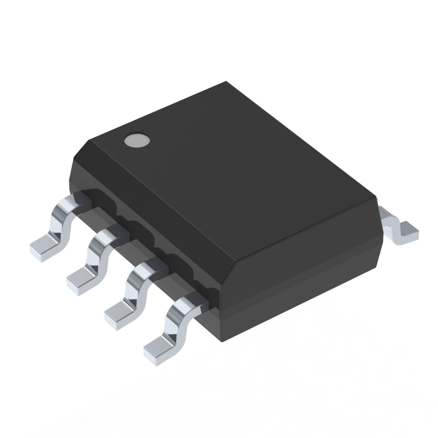
SO-8
A
ID(@TA = 25°C)Q2
12
Applications
Dual SO-8 MOSFET for POL converters in desktop, servers, graphics cards, game consoles
and set-top box
l
Features
Industry-standard pinout SO-8 Package
Compatible with Existing Surface Mount Techniques
RoHS Compliant, Halogen-Free
MSL1, Industrial qualification
Base Part Number
Package Type
IRF9910PbF-1
SO-8
Benefits
Multi-Vendor Compatibility
Easier Manufacturing
Environmentally Friendlier
Increased Reliability
⇒
Standard Pack
Form
Quantity
Tape and Reel
4000
Orderable Part Number
IRF9910TRPbF-1
Absolute Maximum Ratings
Parameter
Q1 Max.
Q2 Max.
VDS
Drain-to-Source Voltage
20
VGS
Gate-to-Source Voltage
Continuous Drain Current, VGS @ 10V
± 20
ID @ TA = 25°C
IDM
Continuous Drain Current, VGS @ 10V
Pulsed Drain Current
ID @ TA = 70°C
c
V
10
12
8.3
9.9
83
98
PD @TA = 25°C
Power Dissipation
2.0
PD @TA = 70°C
Power Dissipation
1.3
TJ
Linear Derating Factor
Operating Junction and
TSTG
Storage Temperature Range
Units
A
W
W/°C
°C
0.016
-55 to + 150
Thermal Resistance
Typ.
Max.
Units
RθJL
Junction-to-Drain Lead
Parameter
–––
42
°C/W
RθJA
Junction-to-Ambient
–––
62.5
fg
Notes through
are on page 11
1
www.irf.com © 2014 International Rectifier
Submit Datasheet Feedback
October 16, 2014
�IRF9910TRPbF-1
Static @ T J = 25°C (unless otherwise specified)
Parameter
BV DSS
ΔΒV DSS /ΔTJ
Drain-to-Source Breakdown Voltage
Breakdown Voltage Temp. Coefficient
R DS(on)
Static Drain-to-Source On-Resistance
Q1&Q2
Q1
Q2
Q1
Q2
V GS(th)
ΔV GS(th)/ΔT J
Gate Threshold Voltage
Gate Threshold Voltage Coefficient
I DSS
Drain-to-Source Leakage Current
I GSS
gfs
Gate-to-Source Forward Leakage
Gate-to-Source Reverse Leakage
Forward Transconductance
Qg
Total Gate Charge
Q gs1
Pre-Vth Gate-to-Source Charge
Q gs2
Post-Vth Gate-to-Source Charge
Q gd
Gate-to-Drain Charge
Q godr
Gate Charge Overdrive
Q sw
Switch Charge (Q gs2 + Q gd)
Q oss
Output Charge
t d(on)
Turn-On Delay Time
tr
Rise Time
t d(off)
Turn-Off Delay Time
tf
Fall Time
C iss
Input Capacitance
C oss
Output Capacitance
C rss
Reverse Transfer Capacitance
Q1&Q2
Q1
Q2
Q1&Q2
Q1&Q2
Q1&Q2
Q1&Q2
Q1
Q2
Q1
Q2
Q1
Q2
Q1
Q2
Q1
Q2
Q1
Q2
Q1
Q2
Q1
Q2
Q1
Q2
Q1
Q2
Q1
Q2
Q1
Q2
Q1
Q2
Q1
Q2
Q1
Q2
Min.
Typ.
Max.
Units
20
–––
–––
–––
–––
–––
–––
1.65
–––
–––
–––
–––
–––
–––
19
27
–––
–––
–––
–––
–––
–––
–––
–––
–––
–––
–––
–––
–––
–––
–––
–––
–––
–––
–––
–––
–––
–––
–––
–––
–––
–––
–––
–––
–––
0.0061
0.014
10.7
14.6
7.4
9.1
–––
-4.9
-5.0
–––
–––
–––
–––
–––
–––
7.4
15
2.6
4.3
0.85
1.4
2.5
5.4
1.5
3.9
3.4
6.8
4.0
8.7
6.3
8.3
10
14
9.2
15
4.5
7.5
900
1860
290
600
140
310
–––
–––
–––
13.4
18.3
9.3
11.3
2.55
–––
–––
1.0
100
100
-100
–––
–––
11
23
–––
–––
–––
–––
–––
–––
–––
–––
–––
–––
–––
–––
–––
–––
–––
–––
–––
–––
–––
–––
–––
–––
–––
–––
–––
–––
V
V/°C
mΩ
V
mV/°C
μA
nA
S
nC
Conditions
V GS = 0V, ID = 250μA
Reference to 25°C, ID = 1mA
e
e
e
e
V GS = 10V, I D = 10A
V GS = 4.5V, ID = 8.3A
V GS = 10V, I D = 12A
V GS = 4.5V, ID = 9.8A
V DS = V GS , ID = 250μA
V DS = 16V, V GS
V DS = 16V, V GS
V GS = 20V
V GS = -20V
V DS = 10V, I D =
V DS = 10V, I D =
= 0V
= 0V, TJ = 125°C
8.3A
9.8A
Q1
V DS = 10V
V GS = 4.5V, ID = 8.3A
Q2
V DS = 10V
V GS = 4.5V, ID = 9.8A
nC
V DS = 10V, V GS = 0V
Q1
V DD = 16V, V GS = 4.5V
ID = 8.3A
ns
Q2
V DD = 16V, V GS = 4.5V
ID = 9.8A
Clamped Inductive Load
pF
V GS = 0V
V DS = 10V
ƒ = 1.0MHz
Avalanche Characteristics
Parameter
Single Pulse Avalanche Energy
E AS
Avalanche Current
I AR
Diode Characteristics
Parameter
c
IS
V SD
Continuous Source Current
(Body Diode)
Pulsed Source Current
(Body Diode)
Diode Forward Voltage
t rr
Reverse Recovery Time
Q rr
Reverse Recovery Charge
I SM
d
�c
2
www.irf.com © 2014 International Rectifier
Typ.
Q1 Max.
Q2 Max.
Units
–––
–––
33
8.3
26
9.8
mJ
A
Min.
Typ.
Max.
Units
Q1&Q2
–––
–––
2.5
A
Q1
Q2
Q1
Q2
Q1
Q2
Q1
Q2
–––
–––
–––
–––
–––
–––
–––
–––
–––
–––
–––
–––
11
16
3.1
4.9
83
98
1.0
1.0
17
24
4.7
7.3
A
V
ns
nC
Submit Datasheet Feedback
Conditions
MOSFET symbol
showing the
G
integral reverse
p-n junction diode.
TJ = 25°C, IS = 8.3A, V GS = 0V
TJ = 25°C, IS = 9.8A, V GS = 0V
Q1 TJ = 25°C, I F = 8.3A,
V DD = 10V, di/dt = 100A/μs
Q2 TJ = 25°C, I F = 9.8A,
V DD = 10V, di/dt = 100A/μs
D
e
e
e
e
October 16, 2014
S
�IRF9910TRPbF-1
Typical Characteristics
Q1 - Control FET
Q2 - Synchronous FET
10000
VGS
10V
8.0V
5.0V
4.5V
4.0V
3.5V
3.0V
2.5V
TOP
1000
100
ID, Drain-to-Source Current (A)
ID, Drain-to-Source Current (A)
10000
BOTTOM
10
1
≤60μs PULSE WIDTH
Tj = 25°C
0.1
2.5V
0.01
0.1
1
10
1000
100
1
2.5V
0.1
100
0.1
1
10
100
V DS, Drain-to-Source Voltage (V)
Fig 2. Typical Output Characteristics
10000
10000
ID, Drain-to-Source Current (A)
ID, Drain-to-Source Current (A)
≤60μs PULSE WIDTH
Tj = 25°C
0.01
Fig 1. Typical Output Characteristics
VGS
10V
8.0V
5.0V
4.5V
4.0V
3.5V
3.0V
2.5V
TOP
1000
BOTTOM
100
10
1
2.5V
≤ 60μs PULSE WIDTH
Tj = 150°C
0.1
0.1
1
10
1000
T = 25°C
J
V
= 10V
DS
≤60μs PULSE WIDTH
0.1
3
4
2.5V
1
≤60μs PULSE WIDTH
Tj = 150°C
0.1
5
6
VGS, Gate-to-Source Voltage (V)
Fig 5. Typical Transfer Characteristics
www.irf.com © 2014 International Rectifier
1
10
100
V DS, Drain-to-Source Voltage (V)
Fig 4. Typical Output Characteristics
ID, Drain-to-Source Current (Α)
T = 150°C
J
10
2
10
0.1
V DS, Drain-to-Source Voltage (V)
1
BOTTOM
100
100
100
VGS
10V
5.0V
4.5V
4.0V
3.5V
3.0V
2.8V
2.5V
TOP
Fig 3. Typical Output Characteristics
ID, Drain-to-Source Current (Α)
BOTTOM
10
V DS, Drain-to-Source Voltage (V)
3
VGS
10V
5.0V
4.5V
4.0V
3.5V
3.0V
2.8V
2.5V
TOP
100
10
T = 25°C
J
T = 150°C
J
1
V
= 10V
DS
≤ 60μs PULSE WIDTH
0.1
1
2
3
4
5
VGS, Gate-to-Source Voltage (V)
Fig 6. Typical Transfer Characteristics
Submit Datasheet Feedback
October 16, 2014
�IRF9910TRPbF-1
Typical Characteristics
Q2 - Synchronous FET
Q1 - Control FET
VGS = 0V,
C, Capacitance(pF)
C
C
C
1000
C
iss
rss
oss
=C
=C
=C
gs
100000
f = 1 MHZ
+ C
gd
, C
ds
gd
ds
+C
gd
iss
C
oss
C
C
oss
=C
=C
gd
ds
+C
gd
iss
C
oss
C
rss
100
10
I = 8.3A
D
V = 16V
DS
V = 10V
DS
4.0
3.0
2.0
1.0
0.0
OPERATION IN THIS AREA LIMITED
BY R (on)
DS
100
10
100μsec
1msec
10msec
1
T = 25°C
A
Tj = 150°C
Single Pulse
0.1
0
1
10
100
1000
VDS, Drain-to-Source Voltage (V)
Fig 11. Maximum Safe Operating Area
www.irf.com © 2014 International Rectifier
I = 9.8A
D
5.0
V = 16V
DS
V = 10V
DS
4.0
3.0
2.0
1.0
0.0
0
5
10
15
20
QG Total Gate Charge (nC)
Fig. 10. Gate-to-Source Voltage vs Typical Gate Charge
ID, Drain-to-Source Current (A)
1000
100
6.0
0 1 2 3 4 5 6 7 8 9 10
QG Total Gate Charge (nC)
Fig. 9. Gate-to-Source Voltage vs Typical Gate Charge
10
VDS, Drain-to-Source Voltage (V)
Fig 8. Typical Capacitance Vs.Drain-to-Source Voltage
VGS, Gate-to-Source Voltage (V)
6.0
5.0
1
100
VDS, Drain-to-Source Voltage (V)
Fig 7. Typical Capacitance Vs.Drain-to-Source Voltage
VGS, Gate-to-Source Voltage (V)
C
1000
rss
rss
1
ID, Drain-to-Source Current (A)
C
10000
100
4
VGS = 0V,
f = 1 MHZ
C
=C
+ C , C
SHORTED
iss
gs
gd
ds
SHORTED
C, Capacitance(pF)
10000
1000
OPERATION IN THIS AREA LIMITED
BY R (on)
DS
100
10
100μsec
1msec
10msec
1
T = 25°C
A
Tj = 150°C
Single Pulse
0.1
0
1
10
100
1000
VDS, Drain-to-Source Voltage (V)
Fig 12. Maximum Safe Operating Area
Submit Datasheet Feedback
October 16, 2014
�IRF9910TRPbF-1
Typical Characteristics
Q1 - Control FET
Q2 - Synchronous FET
R DS(on) , Drain-to-Source On Resistance
R DS(on) , Drain-to-Source On Resistance
1.5
(Normalized)
= 10A
D
V
= 10V
GS
(Normalized)
I
1.0
0.5
I
= 12A
D
V
= 10V
GS
1.0
0.5
-60 -40 -20 0 20 40 60 80 100120140160
-60 -40 -20 0 20 40 60 80 100120140160
TJ , Junction Temperature (°C)
TJ , Junction Temperature (°C)
Fig 13. Normalized On-Resistance vs. Temperature
Fig 14. Normalized On-Resistance vs. Temperature
100
100
ISD, Reverse Drain Current (A)
ISD, Reverse Drain Current (A)
1.5
T = 150°C
J
10
T = 25°C
J
1
T = 150°C
J
10
T = 25°C
J
1
V
= 0V
GS
V
= 0V
GS
0
0
0.2
0.4
0.6
0.8
1.0
1.2
1.4
1.6
0.2
VSD, Source-to-Drain Voltage (V)
0.4
0.6
0.8
1.0
1.2
1.4
1.6
VSD, Source-to-Drain Voltage (V)
Fig 15. Typical Source-Drain Diode Forward Voltage
40
R DS(on), Drain-to -Source On Resistance (m
Ω)
R
, Drain-to -Source On Resistance (m
Ω)
DS(on)
Fig 16. Typical Source-Drain Diode Forward Voltage
I = 10A
D
35
30
25
T = 125°C
J
20
15
10
TJ = 25°C
5
0
2
3
4
5
6
7
8
9
10
VGS, Gate -to -Source Voltage (V)
Fig 17. Typical On-Resistance vs. Gate Voltage
5
www.irf.com © 2014 International Rectifier
25
ID = 12A
20
15
T = 125°C
J
10
T = 25°C
J
5
0
2
3
4
5
6
7
8
9
10
VGS, Gate -to -Source Voltage (V)
Fig 18. Typical On-Resistance vs. Gate Voltage
Submit Datasheet Feedback
October 16, 2014
�IRF9910TRPbF-1
Typical Characteristics
Q2 - Synchronous FET
12
14
10
12
ID , Drain Current (A)
ID , Drain Current (A)
Q1 - Control FET
8
6
4
2
10
8
6
4
2
0
0
25
50
75
100
125
150
25
TA , Ambient Temperature (°C)
Fig 19. Maximum Drain Current vs.
Ambient Temperature
VGS(th) Gate threshold Voltage (V)
2.0
ID = 250μA
1.5
125
150
2.0
ID = 250μA
1.5
1.0
-75 -50 -25
0
25
50
75 100 125 150
-75 -50 -25
TJ , Temperature ( °C )
I
TOP
BOTTOM
100
D
2.2A
2.6A
8.3A
80
60
40
20
0
25
50
75
100
125
25
50
75 100 125 150
Fig 22. Threshold Voltage vs. Temperature
EAS , Single Pulse Avalanche Energy (mJ)
140
120
0
TJ , Temperature ( °C )
Fig 21. Threshold Voltage vs. Temperature
EAS , Single Pulse Avalanche Energy (mJ)
100
2.5
1.0
150
Starting TJ , Junction Temperature (°C)
Fig 23. Maximum Avalanche Energy
vs. Drain Current
6
75
Fig 20. Maximum Drain Current vs.
Ambient Temperature
2.5
VGS(th) Gate threshold Voltage (V)
50
TA , Ambient Temperature (°C)
www.irf.com © 2014 International Rectifier
120
I
TOP
100
BOTTOM
D
5.5A
6.2A
9.8A
80
60
40
20
0
25
50
75
100
125
150
Starting TJ , Junction Temperature (°C)
Fig 24. Maximum Avalanche Energy
vs. Drain Current
Submit Datasheet Feedback
October 16, 2014
�IRF9910TRPbF-1
100
Thermal Response ( Z thJA )
D = 0.50
0.20
0.10
0.05
10
0.02
0.01
1
τJ
0.1
SINGLE PULSE
( THERMAL RESPONSE )
0.01
R1
R1
τJ
τ1
R2
R2
R3
R3
Ri (°C/W)
R4
R4
τC
τ
τ2
τ1
τ3
τ2
τ4
τ3
τ4
Ci= τi/Ri
Ci i/Ri
τi (sec)
1.688
0.000230
14.468
0.105807
30.264
1.001500
16.106
29.90000
Notes:
1. Duty Factor D = t1/t2
2. Peak Tj = P dm x Zthja + Tc
0.001
1E-006
1E-005
0.0001
0.001
0.01
0.1
1
10
100
t1 , Rectangular Pulse Duration (sec)
Fig 25. Maximum Effective Transient Thermal Impedance, Junction-to-Ambient
Current Regulator
Same Type as D.U.T.
50KΩ
V(BR)DSS
12V
.2μF
.3μF
tp
15V
D.U.T.
DRIVER
L
VDS
+
V
- DS
VGS
D.U.T
RG
+
- VDD
IAS
20V
VGS
tp
3mA
A
0.01Ω
I AS
IG
ID
Current Sampling Resistors
Fig 26. Unclamped Inductive Test Circuit
and Waveform
Fig 27. Gate Charge Test Circuit
LD
VDS
VDS
+
90%
V DD D.U.T
VGS
Pulse Width < 1μs
Duty Factor < 0.1%
Fig 28. Switching Time Test Circuit
7
www.irf.com © 2014 International Rectifier
10%
VGS
td(on)
tr
td(off)
tf
Fig 29. Switching Time Waveforms
Submit Datasheet Feedback
October 16, 2014
�IRF9910TRPbF-1
D.U.T
Driver Gate Drive
+
-
-
*
D.U.T. ISD Waveform
Reverse
Recovery
Current
+
RG
• dv/dt controlled by RG
• Driver same type as D.U.T.
• I SD controlled by Duty Factor "D"
• D.U.T. - Device Under Test
P.W.
Period
VGS=10V
Circuit Layout Considerations
• Low Stray Inductance
• Ground Plane
• Low Leakage Inductance
Current Transformer
D=
Period
P.W.
+
V DD
+
-
Body Diode Forward
Current
di/dt
D.U.T. VDS Waveform
Diode Recovery
dv/dt
Re-Applied
Voltage
Body Diode
VDD
Forward Drop
Inductor Curent
ISD
Ripple ≤ 5%
*
VGS = 5V for Logic Level Devices
Fig 30. Peak Diode Recovery dv/dt Test Circuit for N-Channel
HEXFET® Power MOSFETs
Id
Vds
Vgs
Vgs(th)
Qgs1 Qgs2
Qgd
Qgodr
Fig 31. Gate Charge Waveform
8
www.irf.com © 2014 International Rectifier
Submit Datasheet Feedback
October 16, 2014
�IRF9910TRPbF-1
SO-8 Package Outline(Mosfet & Fetky)
Dimensions are shown in milimeters (inches)
D
DIM
B
5
A
8
6
7
6
H
E
1
6X
2
3
0.25 [.010]
4
A
e
e1
0.25 [.010]
MIN
.0532
.0688
1.35
1.75
MAX
A1 .0040
0.25
.0098
0.10
b
.013
.020
0.33
0.51
c
.0075
.0098
0.19
0.25
D
.189
.1968
4.80
5.00
E
.1497
.1574
3.80
4.00
e
.050 BAS IC
1.27 BASIC
e1
.025 BAS IC
0.635 BAS IC
H
.2284
.2440
5.80
6.20
K
.0099
.0196
0.25
0.50
L
.016
.050
0.40
1.27
y
0°
8°
0°
8°
K x 45°
A
C
8X b
MILLIMETERS
MAX
A
5
INCHES
MIN
A1
y
0.10 [.004]
8X c
8X L
7
C A B
FOOT PRINT
NOT ES:
1. DIMENS IONING & T OLERANCING PER AS ME Y14.5M-1994.
2. CONT ROLLING DIMENSION: MILLIMET ER
8X 0.72 [.028]
3. DIMENS IONS ARE S HOWN IN MILLIMET ERS [INCHES ].
4. OUT LINE CONFORMS T O JEDEC OUT LINE MS-012AA.
5 DIMENS ION DOES NOT INCLUDE MOLD PROT RUS IONS .
MOLD PROT RUSIONS NOT T O EXCEED 0.15 [.006].
6 DIMENS ION DOES NOT INCLUDE MOLD PROT RUS IONS .
MOLD PROT RUSIONS NOT T O EXCEED 0.25 [.010].
6.46 [.255]
7 DIMENS ION IS T HE LENGT H OF LEAD FOR S OLDERING T O
A S UBS T RAT E.
3X 1.27 [.050]
8X 1.78 [.070]
SO-8 Part Marking Information
EXAMPLE: T HIS IS AN IRF7101 (MOSFET)
INT ERNATIONAL
RECTIFIER
LOGO
XXXX
F 7101
DAT E CODE (YWW)
P = DIS GNATES LEAD - FREE
PRODUCT (OPT IONAL)
Y = LAST DIGIT OF THE YEAR
WW = WEEK
A = AS S EMBLY S ITE CODE
LOT CODE
PART NUMBER
Note: For the most current drawing please refer to IR website at: http://www.irf.com/package/
9
www.irf.com © 2014 International Rectifier
Submit Datasheet Feedback
October 16, 2014
�IRF9910TRPbF-1
SO-8 Tape and Reel (Dimensions are shown in millimeters (inches))
TERMINAL NUMBER 1
12.3 ( .484 )
11.7 ( .461 )
8.1 ( .318 )
7.9 ( .312 )
FEED DIRECTION
NOTES:
1. CONTROLLING DIMENSION : MILLIMETER.
2. ALL DIMENSIONS ARE SHOWN IN MILLIMETERS(INCHES).
3. OUTLINE CONFORMS TO EIA-481 & EIA-541.
330.00
(12.992)
MAX.
14.40 ( .566 )
12.40 ( .488 )
NOTES :
1. CONTROLLING DIMENSION : MILLIMETER.
2. OUTLINE CONFORMS TO EIA-481 & EIA-541.
Note: For the most current drawing please refer to IR website at: http://www.irf.com/package/
10
www.irf.com © 2014 International Rectifier
Submit Datasheet Feedback
October 16, 2014
�IRF9910TRPbF-1
†
Qualification information
Industrial
Qualification level
(per JEDE C JE S D47F
Moisture Sensitivity Level
SO-8
RoHS compliant
††
guidelines)
MS L1
††
(per JEDE C J-S T D-020D )
Yes
† Qualification standards can be found at International Rectifier’s web site: http://www.irf.com/product-info/reliability
†† Applicable version of JEDEC standard at the time of product release
Notes:
Repetitive rating; pulse width limited by max. junction temperature.
Starting TJ = 25°C, Q1: L = 0.95mH, RG = 25Ω, IAS = 8.3A; Q2: L = 0.54mH, RG = 25Ω, IAS = 9.8A.
Pulse width ≤ 400μs; duty cycle ≤ 2%.
When mounted on 1 inch square copper board.
Rθ is measured at TJ approximately 90°C.
Revision History
Date
10/16/2014
Comments
• Corrected part number from" IRF9910PbF-1" to "IRF9910TRPbF-1" -all pages
• Removed the "IRF9910PbF-1" bulk part number from ordering information on page1
IR WORLD HEADQUARTERS: 101 N. Sepulveda Blvd., El Segundo, California 90245, USA
To contact International Rectifier, please visit http://www.irf.com/whoto-call/
11
www.irf.com © 2014 International Rectifier
Submit Datasheet Feedback
October 16, 2014
�


 工商网监
湘ICP备2023018690号
工商网监
湘ICP备2023018690号
