PD - 95135
IRF9952PbF
l
l
l
l
l
l
l
HEXFET® Power MOSFET
Generation V Technology
Ultra Low On-Resistance
Dual N and P Channel MOSFET
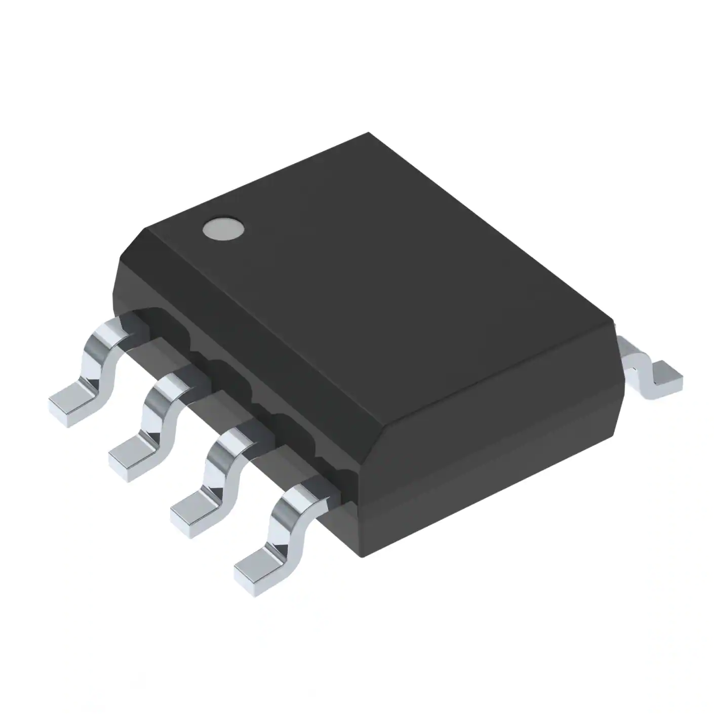
Surface Mount
Very Low Gate Charge and
Switching Losses
Fully Avalanche Rated
Lead-Free
S1
G1
S2
G2
N-CHANNEL MOSFET
1
8
2
7
D1
3
6
D2
4
5
D2
VDSS
Top View
Fifth Generation HEXFETs from International Rectifier
utilize advanced processing techniques to achieve
extremely low on-resistance per silicon area. This
benefit, combined with the fast switching speed and
ruggedized device design that HEXFET Power
MOSFETs are well known for, provides the designer
with an extremely efficient and reliable device for use
in a wide variety of applications.
SO-8
Symbol
TA = 25°C
TA = 70°C
Pulsed Drain Current
Continuous Source Current (Diode Conduction)
TA = 25°C
Maximum Power Dissipation
TA = 70°C
Single Pulse Avalanche Energy
Avalanche Current
Repetitive Avalanche Energy
Peak Diode Recovery dv/dt
Junction and Storage Temperature Range
-30V
Recommended upgrade: IRF7309 or IRF7319
Lower profile/smaller equivalent: IRF7509
The SO-8 has been modified through a customized
leadframe for enhanced thermal characteristics and
multiple-die capability making it ideal in a variety of
power applications. With these improvements, multiple
devices can be used in an application with dramatically
reduced board space. The package is designed for
vapor phase, infra red, or wave soldering techniques.
Drain-Source Voltage
Gate-Source Voltage
30V
RDS(on) 0.10Ω 0.25Ω
P-CHANNEL MOSFET
Description
Continuous Drain Current
N-Ch P-Ch
D1
V DS
V GS
ID
IDM
IS
Maximum
P-Channel
N-Channel
30
± 20
3.5
2.8
16
1.7
EAS
IAR
EAR
dv/dt
TJ, TSTG
V
-2.3
-1.8
-10
-1.3
2.0
1.3
PD
44
2.0
Units
A
W
57
-1.3
0.25
mJ
A
mJ
V/ ns
5.0
-5.0
-55 to + 150 °C
Symbol
Limit
Units
RθJA
62.5
°C/W
Thermal Resistance Ratings
Parameter
Maximum Junction-to-Ambient
www.irf.com
1
09/15/04
�IRF9952PbF
Electrical Characteristics @ TJ = 25°C (unless otherwise specified)
Parameter
V (BR)DSS
Drain-to-Source Breakdown Voltage
∆V(BR)DSS/∆TJ Breakdown Voltage Temp. Coefficient
RDS(ON)
Static Drain-to-Source On-Resistance
V GS(th)
Gate Threshold Voltage
gfs
Forward Transconductance
I DSS
Drain-to-Source Leakage Current
I GSS
Gate-to-Source Forward Leakage
Qg
Total Gate Charge
Qgs
Gate-to-Source Charge
Qgd
Gate-to-Drain ("Miller") Charge
td(on)
Turn-On Delay Time
tr
Rise Time
td(off)
Turn-Off Delay Time
tf
Fall Time
Ciss
Input Capacitance
Coss
Output Capacitance
Crss
Reverse Transfer Capacitance
Min.
30
-30
1.0
-1.0
N-Ch
P-Ch
N-Ch
P-Ch
N-Ch
P-Ch
N-Ch
P-Ch
N-Ch
P-Ch
N-Ch
P-Ch
N-Ch
P-Ch
N-P
N-Ch
P-Ch
N-Ch
P-Ch
N-Ch
P-Ch
N-Ch
P-Ch
N-Ch
P-Ch
N-Ch
P-Ch
N-Ch
P-Ch
N-Ch
P-Ch
N-Ch
P-Ch
N-Ch
P-Ch
Typ. Max.
0.015
0.015
0.08 0.10
0.12 0.15
0.165 0.250
0.290 0.400
12
2.4
2.0
-2.0
25
-25
±100
6.9 14
6.1 12
1.0 2.0
1.7 3.4
1.8 3.5
1.1 2.2
6.2 12
9.7 19
8.8 18
14
28
13
26
20
40
3.0 6.0
6.9 14
190
190
120
110
61
54
Units
V
V/°C
Ω
V
S
µA
nA
nC
ns
pF
Conditions
VGS = 0V, ID = 250µA
VGS = 0V, ID = -250µA
Reference to 25°C, ID = 1mA
Reference to 25°C, ID = -1mA
VGS = 10V, ID = 2.2A
VGS = 4.5V, ID = 1.0A
VGS = -10V, ID = -1.0A
VGS = -4.5V, ID = -0.50A
VDS = VGS, I D = 250µA
VDS = VGS, I D = -250µA
VDS = 15V, I D = 3.5A
VDS = -15V, I D = -2.3A
VDS = 24V, V GS = 0V
VDS = -24V, VGS = 0V
VDS = 24V, V GS = 0V, TJ = 125°C
VDS = -24V, VGS = 0V, TJ = 125°C
VGS = ±20V
N-Channel
I D = 1.8A, VDS = 10V, VGS = 10V
P-Channel
I D = -2.3A, V DS = -10V, VGS = -10V
N-Channel
VDD = 10V, ID = 1.0A, R G = 6.0Ω,
RD = 10Ω
P-Channel
VDD = -10V, ID = -1.0A, RG = 6.0Ω,
RD = 10Ω
N-Channel
V GS = 0V, VDS = 15V, = 1.0MHz
P-Channel
V GS = 0V, VDS = -15V, = 1.0MHz
Source-Drain Ratings and Characteristics
Parameter
IS
Continuous Source Current (Body Diode)
ISM
Pulsed Source Current (Body Diode)
VSD
Diode Forward Voltage
trr
Reverse Recovery Time
Qrr
Reverse Recovery Charge
N-Ch
P-Ch
N-Ch
P-Ch
N-Ch
P-Ch
N-Ch
P-Ch
N-Ch
P-Ch
Min. Typ. Max. Units
Conditions
1.7
-1.3
A
16
16
0.82 1.2
TJ = 25°C, IS = 1.25A, V GS = 0V
V
-0.82 -1.2
TJ = 25°C, IS = -1.25A, VGS = 0V
27
53
N-Channel
ns
27
54
TJ = 25°C, IF =1.25A, di/dt = 100A/µs
28
57
P-Channel
nC
TJ = 25°C, IF = -1.25A, di/dt = 100A/µs
31
62
Notes:
Repetitive rating; pulse width limited by
Pulse width ≤ 300µs; duty cycle ≤ 2%.
max. junction temperature. ( See fig. 23 )
Surface mounted on FR-4 board, t ≤ 10sec.
N-Channel ISD ≤ 2.0A, di/dt ≤ 100A/µs, VDD ≤ V(BR)DSS, TJ ≤ 150°C
P-Channel ISD ≤ -1.3A, di/dt ≤ 84A/µs, VDD ≤ V(BR)DSS, TJ ≤ 150°C
N-Channel Starting TJ = 25°C, L = 22mH RG = 25Ω, IAS = 2.0A. (See Figure 12)
P-Channel Starting TJ = 25°C, L = 67mH RG = 25Ω, IAS = -1.3A.
2
www.irf.com
�IRF9952PbF
N-Channel
100
100
VGS
15V
10V
7.0V
5.5V
4.5V
4.0V
3.5V
BOTTOM 3.0V
VGS
15V
10V
7.0V
5.5V
4.5V
4.0V
3.5V
BOTTOM 3.0V
TOP
I D, Drain-to-Source Current (A)
I D , Drain-to-Source Current (A)
TOP
10
3.0V
20µs PULSE WIDTH
TJ = 25°C
A
1
0.1
1
10
3.0V
20µs PULSE WIDTH
TJ = 150°C
A
1
10
0.1
V DS , Drain-to-Source Voltage (V)
Fig 1. Typical Output Characteristics
10
Fig 2. Typical Output Characteristics
100
ISD , Reverse Drain Current (A)
100
I D , Drain-to-Source Current (A)
1
VDS , Drain-to-Source Voltage (V)
TJ = 25°C
10
TJ = 150°C
V DS = 10V
20µs PULSE WIDTH
1
3.0
3.5
4.0
4.5
5.0
5.5
VGS , Gate-to-Source Voltage (V)
Fig 3. Typical Transfer Characteristics
www.irf.com
A
6.0
10
TJ = 150°C
TJ = 25°C
1
VGS = 0V
0.1
0.4
0.6
0.8
1.0
1.2
A
1.4
VSD , Source-to-Drain Voltage (V)
Fig 4. Typical Source-Drain Diode
Forward Voltage
3
�IRF9952PbF
RDS (on) , Drain-to-Source On Resistance (Ω)
RDS(on) , Drain-to-Source On Resistance
(Normalized)
2.0
N-Channel
ID = 2.2A
1.5
1.0
0.5
0.0
-60 -40 -20
VGS = 10V
0
20
40
60
0.12
0.10
VGS = 4.5V
0.08
VGS = 10V
0.06
0.04
80 100 120 140 160
0
2
TJ , Junction Temperature ( °C)
0.12
0.10
0.08
I D = 3.5A
0.06
0.04
0.02
0.00
A
9
12
V GS , Gate-to-Source Voltage (V)
Fig 7. Typical On-Resistance Vs. Gate
Voltage
4
E AS , Single Pulse Avalanche Energy (mJ)
RDS (on) , Drain-to-Source On Resistance (Ω)
0.14
6
8
10
12
A
Fig 6. Typical On-Resistance Vs. Drain
Current
0.16
3
6
I D , Drain Current (A)
Fig 5. Normalized On-Resistance
Vs. Temperature
0
4
15
100
TOP
BOTTOM
80
ID
0.89A
1.6A
2.0A
60
40
20
A
0
25
50
75
100
125
150
Starting T J , Junction Temperature (°C)
Fig 8. Maximum Avalanche Energy
Vs. Drain Current
www.irf.com
�IRF9952PbF
N-Channel
350
250
VGS , Gate-to-Source Voltage (V)
300
C, Capacitance (pF)
20
V GS = 0V,
f = 1MHz
C iss = Cgs + C gd , Cds SHORTED
C rss = C gd
C oss = C ds + C gd
Ciss
Coss
200
150
Crss
100
50
0
A
1
10
100
ID = 1.8A
VDS = 10V
16
12
8
4
0
0
2
4
6
8
10
QG , Total Gate Charge (nC)
VDS , Drain-to-Source Voltage (V)
Fig 9. Typical Capacitance Vs.
Drain-to-Source Voltage
Fig 10. Typical Gate Charge Vs.
Gate-to-Source Voltage
Thermal Response (Z thJA )
100
0.50
0.20
10
0.10
0.05
0.02
1
PDM
0.01
t1
t2
SINGLE PULSE
(THERMAL RESPONSE)
0.1
0.00001
0.0001
0.001
Notes:
1. Duty factor D = t 1 / t 2
2. Peak T J = P DM x Z thJA + TA
0.01
0.1
1
10
100
t1 , Rectangular Pulse Duration (sec)
Fig 11. Maximum Effective Transient Thermal Impedance, Junction-to-Ambient
www.irf.com
5
�IRF9952PbF
100
P-Channel
100
VGS
- 15V
- 10V
- 7.0V
- 5.5V
- 4.5V
- 4.0V
- 3.5V
BOTTOM - 3.0V
VGS
- 15V
- 10V
- 7.0V
- 5.5V
- 4.5V
- 4.0V
- 3.5V
BOTTOM - 3.0V
TOP
-I D , Drain-to-Source Current (A)
-I D , Drain-to-Source Current (A)
TOP
10
1
-3.0V
20µs PULSE WIDTH
TJ = 25°C
A
0.1
0.1
1
10
1
-3.0V
20µs PULSE WIDTH
TJ = 150°C
A
0.1
10
0.1
-VDS , Drain-to-Source Voltage (V)
Fig 12. Typical Output Characteristics
100
-ISD , Reverse Drain Current (A)
-ID , Drain-to-Source Current (A)
10
Fig 13. Typical Output Characteristics
100
10
TJ = 25°C
T J = 150°C
1
VDS = -10V
20µs PULSE WIDTH
0.1
3.0
4.0
5.0
6.0
7.0
8.0
-VGS , Gate-to-Source Voltage (V)
Fig 14. Typical Transfer Characteristics
6
1
-VDS , Drain-to-Source Voltage (V)
A
10
TJ = 150°C
TJ = 25°C
1
VGS = 0V
0.1
0.4
0.6
0.8
1.0
1.2
A
1.4
-VSD , Source-to-Drain Voltage (V)
Fig 15. Typical Source-Drain Diode
Forward Voltage
www.irf.com
�IRF9952PbF
R DS(on) , Drain-to-Source On Resistance
(Normalized)
2.0
RDS(on) , Drain-to-Source On Resistance ( Ω )
P-Channel
ID = -1.0A
1.5
1.0
0.5
0.0
-60 -40 -20
VGS = -10V
0
20
40
60
2.0
1.5
VGS = -4.5V
1.0
0.5
VGS = -10V
0.0
80 100 120 140 160
A
0.0
TJ , Junction Temperature ( °C)
1.0
2.0
3.0
150
EAS , Single Pulse Avalanche Energy (mJ)
0.60
I D = -2.3A
0.20
0.00
A
0
3
6
9
12
-V GS , Gate-to-Source Voltage (V)
Fig 18. Typical On-Resistance Vs. Gate
Voltage
www.irf.com
5.0
Fig 17. Typical On-Resistance Vs. Drain
Current
0.80
0.40
4.0
-I D , Drain Current (A)
Fig 16. Normalized On-Resistance
Vs. Temperature
RDS(on) , Drain-to-Source On Resistance ( Ω )
2.5
15
ID
-0.58A
-1.0A
BOTTOM -1.3A
TOP
120
90
60
30
0
25
50
75
100
125
150
Starting TJ , Junction Temperature ( °C)
Fig 19. Maximum Avalanche Energy
Vs. Drain Current
7
�IRF9952PbF
400
P-Channel
20
-VGS , Gate-to-Source Voltage (V)
V GS = 0V,
f = 1MHz
C iss = Cgs + C gd , Cds SHORTED
C rss = C gd
C oss = C ds + C gd
C, Capacitance (pF)
300
Ciss
Coss
200
Crss
100
0
A
1
10
100
ID = -2.3A
VDS =-10V
16
12
8
4
0
0
2
4
6
8
10
QG , Total Gate Charge (nC)
-VDS , Drain-to-Source Voltage (V)
Fig 21. Typical Gate Charge Vs.
Gate-to-Source Voltage
Fig 20. Typical Capacitance
Vs.
Drain-to-Source Voltage
Thermal Response (Z thJA )
100
0.50
0.20
10
0.10
0.05
0.02
1
PDM
0.01
t1
t2
SINGLE PULSE
(THERMAL RESPONSE)
0.1
0.00001
0.0001
0.001
Notes:
1. Duty factor D = t 1 / t 2
2. Peak T J = P DM x Z thJA + TA
0.01
0.1
1
10
100
t1 , Rectangular Pulse Duration (sec)
Fig 22. Maximum Effective Transient Thermal Impedance, Junction-to-Ambient
8
www.irf.com
�IRF9952PbF
SO-8 Package Outline
Dimensions are shown in millimeters (inches)
D
5
A
8
6
7
6
5
H
0.25 [.010]
1
6X
2
3
A
4
e
e1
MAX
MIN
.0532
.0688
1.35
1.75
C
A1 .0040
.0098
0.10
0.25
b
.013
.020
0.33
0.51
c
.0075
.0098
0.19
0.25
D
.189
.1968
4.80
5.00
E
.1497
.1574
3.80
4.00
e
.050 BAS IC
e1
1.27 BAS IC
.025 BAS IC
0.635 BAS IC
H
.2284
.2440
5.80
6.20
K
.0099
.0196
0.25
0.50
L
.016
.050
0.40
1.27
y
0°
8°
0°
8°
y
0.10 [.004]
0.25 [.010]
MAX
K x 45°
A
8X b
MILLIMET ERS
MIN
A
E
INCHES
DIM
B
A1
8X L
8X c
7
C A B
F OOT PRINT
NOT ES :
1. DIMENS IONING & T OLE RANCING PE R AS ME Y14.5M-1994.
8X 0.72 [.028]
2. CONT ROLLING DIME NS ION: MILLIMET ER
3. DIMENS IONS ARE S HOWN IN MILLIMET E RS [INCHES ].
4. OUT LINE CONFORMS T O JEDE C OUT LINE MS -012AA.
5 DIMENS ION DOES NOT INCLUDE MOLD PROT RUS IONS .
MOLD PROT RUS IONS NOT T O EXCE ED 0.15 [.006].
6 DIMENS ION DOES NOT INCLUDE MOLD PROT RUS IONS .
MOLD PROT RUS IONS NOT T O EXCE ED 0.25 [.010].
6.46 [.255]
7 DIMENS ION IS T HE LE NGT H OF LEAD FOR S OLDERING T O
A S UB S T RAT E.
3X 1.27 [.050]
8X 1.78 [.070]
SO-8 Part Marking
EXAMPLE : T HIS IS AN IRF 7101 (MOS FET )
INT ERNAT IONAL
RECT IF IER
LOGO
XXXX
F7101
DAT E CODE (YWW)
P = DES IGNAT ES LEAD-FREE
PRODUCT (OPT IONAL)
Y = LAS T DIGIT OF T HE YEAR
WW = WEEK
A = AS S EMBLY S IT E CODE
LOT CODE
PART NUMBER
www.irf.com
9
�IRF9952PbF
SO-8 Tape and Reel
Dimensions are shown in millimeters (inches)
TERMINAL NUMBER 1
12.3 ( .484 )
11.7 ( .461 )
8.1 ( .318 )
7.9 ( .312 )
FEED DIRECTION
NOTES:
1. CONTROLLING DIMENSION : MILLIMETER.
2. ALL DIMENSIONS ARE SHOWN IN MILLIMETERS(INCHES).
3. OUTLINE CONFORMS TO EIA-481 & EIA-541.
330.00
(12.992)
MAX.
14.40 ( .566 )
12.40 ( .488 )
NOTES :
1. CONTROLLING DIMENSION : MILLIMETER.
2. OUTLINE CONFORMS TO EIA-481 & EIA-541.
Data and specifications subject to change without notice.
This product has been designed and qualified for the Consumer market.
Qualifications Standards can be found on IR’s Web site.
IR WORLD HEADQUARTERS: 233 Kansas St., El Segundo, California 90245, USA Tel: (310) 252-7105
TAC Fax: (310) 252-7903
Visit us at www.irf.com for sales contact information.09/04
10
www.irf.com
�


 工商网监
湘ICP备2023018690号
工商网监
湘ICP备2023018690号
