PD - 96065
IRFR3706CPbF
IRFU3706CPbF
SMPS MOSFET
Applications
High Frequency Isolated DC-DC
Converters with Synchronous Rectification
for Telecom and Industrial Use
l High Frequency Buck Converters for
Computer Processor Power
l Lead-Free
HEXFET® Power MOSFET
l
VDSS
RDS(on) max
ID
20V
9.0mΩ
75A
Benefits
l
l
l
Ultra-Low Gate Impedance
Very Low RDS(on) at 4.5V VGS
Fully Characterized Avalanche Voltage
and Current
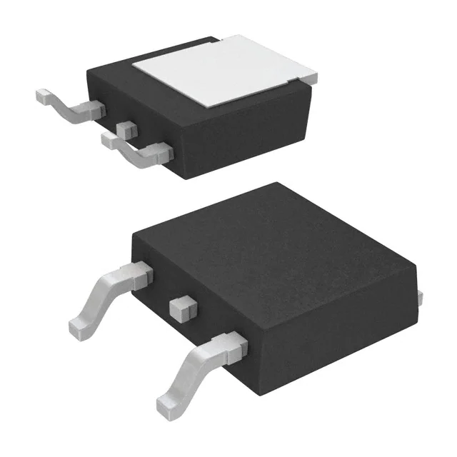
D-Pak
IRFR3706CPbF
I-Pak
IRFU3706CPbF
Absolute Maximum Ratings
Symbol
VDS
VGS
ID @ TC = 25°C
ID @ TC = 100°C
IDM
PD @TC = 25°C
PD @TC = 100°C
TJ , TSTG
Parameter
Drain-Source Voltage
Gate-to-Source Voltage
Continuous Drain Current, VGS @ 10V
Continuous Drain Current, VGS @ 10V
Pulsed Drain Current
Maximum Power Dissipation
Maximum Power Dissipation
Linear Derating Factor
Junction and Storage Temperature Range
Max.
Units
20
± 12
75
53
280
88
44
0.59
-55 to + 175
V
V
A
W
W
mW/°C
°C
Thermal Resistance
Parameter
RθJC
RθJA
RθJA
Junction-to-Case
Junction-to-Ambient (PCB mount)*
Junction-to-Ambient
Typ.
Max.
Units
–––
–––
–––
1.7
50
110
°C/W
* When mounted on 1" square PCB (FR-4 or G-10 Material) .
For recommended footprint and soldering techniques refer to application note #AN-994
Notes through
are on page 10
www.irf.com
1
06/02/06
�IRFR/U3706CPbF
Static @ TJ = 25°C (unless otherwise specified)
Parameter
Drain-to-Source Breakdown Voltage
∆V(BR)DSS/∆TJ Breakdown Voltage Temp. Coefficient
V(BR)DSS
RDS(on)
VGS(th)
IDSS
IGSS
Min.
20
–––
–––
Static Drain-to-Source On-Resistance –––
–––
Gate Threshold Voltage
0.6
–––
Drain-to-Source Leakage Current
–––
Gate-to-Source Forward Leakage
–––
Gate-to-Source Reverse Leakage
–––
Typ.
–––
0.021
6.9
8.1
11.5
–––
–––
–––
–––
–––
Max. Units
––– V
––– V/°C
9.0
11 mΩ
23
2.0
V
20
µA
100
200
nA
-200
Conditions
VGS = 0V, ID = 250µA
Reference to 25°C, I D = 1mA
VGS = 10V, ID = 15A
VGS = 4.5V, ID = 12A
VGS = 2.8V, ID = 7.5A
VDS = VGS, ID = 250µA
VDS = 16V, VGS = 0V
VDS = 16V, VGS = 0V, TJ = 125°C
VGS = 12V
VGS = -12V
Dynamic @ TJ = 25°C (unless otherwise specified)
Symbol
gfs
Qg
Qgs
Qgd
Qoss
Rg
td(on)
tr
td(off)
tf
Ciss
Coss
Crss
Parameter
Forward Transconductance
Total Gate Charge
Gate-to-Source Charge
Gate-to-Drain ("Miller") Charge
Output Gate Charge
Gate Resistance
Turn-On Delay Time
Rise Time
Turn-Off Delay Time
Fall Time
Input Capacitance
Output Capacitance
Reverse Transfer Capacitance
Min.
53
–––
–––
–––
–––
–––
–––
–––
–––
–––
–––
–––
–––
Typ.
–––
23
8.0
5.5
16
1.8
6.8
87
17
4.8
2410
1070
140
Max. Units
Conditions
–––
S
VDS = 16V, ID = 57A
35
ID = 28A
12
nC
VDS = 10V
8.3
VGS = 4.5V
24
VGS = 0V, VDS = 10V
–––
Ω
–––
VDD = 10V
ns
–––
ID = 28A
–––
RG = 1.8Ω
–––
VGS = 4.5V
–––
VGS = 0V
–––
pF
VDS = 10V
–––
ƒ = 1.0MHz
Avalanche Characteristics
Symbol
EAS
IAR
Parameter
Single Pulse Avalanche Energy
Avalanche Current
Typ.
Max.
Units
–––
–––
220
28
mJ
A
Diode Characteristics
Symbol
IS
ISM
Parameter
Continuous Source Current
(Body Diode)
Pulsed Source Current
(Body Diode)
VSD
Diode Forward Voltage
trr
Qrr
trr
Qrr
Reverse
Reverse
Reverse
Reverse
2
Recovery
Recovery
Recovery
Recovery
Time
Charge
Time
Charge
Min. Typ. Max. Units
–––
–––
75
–––
–––
280
–––
–––
–––
–––
–––
–––
0.88
0.82
45
65
49
78
1.3
–––
68
98
74
120
A
V
ns
nC
ns
nC
Conditions
D
MOSFET symbol
showing the
G
integral reverse
S
p-n junction diode.
TJ = 25°C, IS = 36A, VGS = 0V
TJ = 125°C, I S = 36A, VGS = 0V
TJ = 25°C, I F = 36A, VR=20V
di/dt = 100A/µs
TJ = 125°C, IF = 36A, VR=20V
di/dt = 100A/µs
www.irf.com
�IRFR/U3706CPbF
1000
1000
VGS
10V
4.5V
3.7V
3.5V
3.3V
3.0V
2.7V
BOTTOM 2.5V
100
2.5V
20µs PULSE WIDTH
TJ = 25 °C
10
0.1
1
10
100
2.5V
2.0
R DS(on) , Drain-to-Source On Resistance
(Normalized)
I D , Drain-to-Source Current (A)
TJ = 25 ° C
TJ = 175 ° C
100
V DS = 15V
20µs PULSE WIDTH
4.5
5.5
Fig 3. Typical Transfer Characteristics
www.irf.com
10
100
Fig 2. Typical Output Characteristics
1000
3.5
1
VDS , Drain-to-Source Voltage (V)
Fig 1. Typical Output Characteristics
VGS , Gate-to-Source Voltage (V)
20µs PULSE WIDTH
TJ = 175 °C
10
0.1
100
VDS , Drain-to-Source Voltage (V)
10
2.5
VGS
10V
4.5V
3.7V
3.5V
3.3V
3.0V
2.7V
BOTTOM 2.5V
TOP
I D , Drain-to-Source Current (A)
I D , Drain-to-Source Current (A)
TOP
6.5
ID = 71A
1.5
1.0
0.5
0.0
-60 -40 -20 0
VGS = 10V
20 40 60 80 100 120 140 160 180
TJ , Junction Temperature ( °C)
Fig 4. Normalized On-Resistance
Vs. Temperature
3
�IRFR/U3706CPbF
VGS = 0V,
f = 1 MHZ
Ciss = Cgs + Cgd, Cds SHORTED
Crss = Cgd
Coss = Cds + Cgd
C, Capacitance(pF)
10000
Ciss
Coss
1000
Crss
100
VGS , Gate-to-Source Voltage (V)
10
100000
10
ID = 28A
VDS = 16V
VDS = 10V
8
6
4
2
0
1
10
0
100
10
VDS, Drain-to-Source Voltage (V)
1000
ISD , Reverse Drain Current (A)
30
40
50
Fig 6. Typical Gate Charge Vs.
Gate-to-Source Voltage
Fig 5. Typical Capacitance Vs.
Drain-to-Source Voltage
1000
OPERATION IN THIS AREA LIMITED
BY RDS(on)
10us
I D , Drain Current (A)
100
TJ = 175 ° C
10
TJ = 25 ° C
100
100us
1ms
10
10ms
1
0.1
0.2
V GS = 0 V
0.6
1.0
1.4
VSD ,Source-to-Drain Voltage (V)
Fig 7. Typical Source-Drain Diode
Forward Voltage
4
20
QG , Total Gate Charge (nC)
1.8
TC = 25 ° C
TJ = 175° C
Single Pulse
1
1
10
100
VDS, Drain-to-Source Voltage (V)
Fig 8. Maximum Safe Operating Area
www.irf.com
�IRFR/U3706CPbF
80
V DS
LIMITED BY PACKAGE
ID , Drain Current (A)
VGS
D.U.T.
RG
60
RD
+
-VDD
4.5V
Pulse Width ≤ 1 µs
Duty Factor ≤ 0.1 %
40
Fig 10a. Switching Time Test Circuit
20
VDS
90%
0
25
50
75
100
125
150
175
TC , Case Temperature ( °C)
10%
VGS
Fig 9. Maximum Drain Current Vs.
Case Temperature
td(on)
tr
t d(off)
tf
Fig 10b. Switching Time Waveforms
Thermal Response (Z thJC )
10
1 D = 0.50
0.20
0.10
PDM
0.05
0.1
0.02
0.01
0.01
0.00001
t1
SINGLE PULSE
(THERMAL RESPONSE)
t2
Notes:
1. Duty factor D = t 1 / t 2
2. Peak T J = P DM x Z thJC + TC
0.0001
0.001
0.01
0.1
t1 , Rectangular Pulse Duration (sec)
Fig 11. Maximum Effective Transient Thermal Impedance, Junction-to-Case
www.irf.com
5
�15V
DRIVER
L
VDS
D.U.T
RG
+
V
- DD
IAS
20V
tp
A
0.01Ω
Fig 12a. Unclamped Inductive Test Circuit
V(BR)DSS
tp
EAS , Single Pulse Avalanche Energy (mJ)
IRFR/U3706CPbF
500
TOP
400
BOTTOM
ID
12A
24A
28A
300
200
100
0
25
50
75
100
125
150
175
Starting TJ , Junction Temperature ( °C)
Fig 12c. Maximum Avalanche Energy
Vs. Drain Current
I AS
Fig 12b. Unclamped Inductive Waveforms
Current Regulator
Same Type as D.U.T.
QG
4.5 V
50KΩ
12V
.2µF
.3µF
QGS
QGD
D.U.T.
VG
+
V
- DS
VGS
3mA
Charge
Fig 13a. Basic Gate Charge Waveform
6
IG
ID
Current Sampling Resistors
Fig 13b. Gate Charge Test Circuit
www.irf.com
�IRFR/U3706CPbF
Peak Diode Recovery dv/dt Test Circuit
Circuit Layout Considerations
• Low Stray Inductance
• Ground Plane
• Low Leakage Inductance
Current Transformer
+
D.U.T
+
-
-
+
RG
•
•
•
•
dv/dt controlled by RG
Driver same type as D.U.T.
ISD controlled by Duty Factor "D"
D.U.T. - Device Under Test
Driver Gate Drive
P.W.
Period
D=
+
-
VDD
P.W.
Period
VGS=10V
*
D.U.T. ISD Waveform
Reverse
Recovery
Current
Body Diode Forward
Current
di/dt
D.U.T. VDS Waveform
Diode Recovery
dv/dt
Re-Applied
Voltage
Body Diode
VDD
Forward Drop
Inductor Curent
Ripple ≤ 5%
ISD
* VGS = 5V for Logic Level Devices
Fig 14. For N-Channel HEXFET® Power MOSFETs
www.irf.com
7
�IRFR/U3706CPbF
D-Pak (TO-252AA) Package Outline
Dimensions are shown in millimeters (inches)
D-Pak (TO-252AA) Part Marking Information
(;$03/(�
7+,6�,6�$1�,5)5���
3$57�180%(5
:,7+�$66(0%/<
,17(51$7,21$/
/27�&2'(�����
,5)5���
���$
��
��
5(&7,),(5
$66(0%/('�21�::���������
/2*2
,1�7+(�$66(0%/


 工商网监
湘ICP备2023018690号
工商网监
湘ICP备2023018690号
