PD - 97407
IRLB3813PbF
HEXFET® Power MOSFET
Applications
l
Optimized for UPS/Inverter Applications
l
High Frequency Isolated DC-DC
Converters with Synchronous Rectification
for Telecom and Industrial Use
Power Tools
l
Benefits
l Very Low RDS(on) at 4.5V VGS
l Ultra-Low Gate Impedance
l Fully Characterized Avalanche Voltage
and Current
l Lead-Free
VDSS
RDS(on) max
Qg (typ.)
30V 1.95mΩ@VGS = 10V 57nC
D
G
D
S
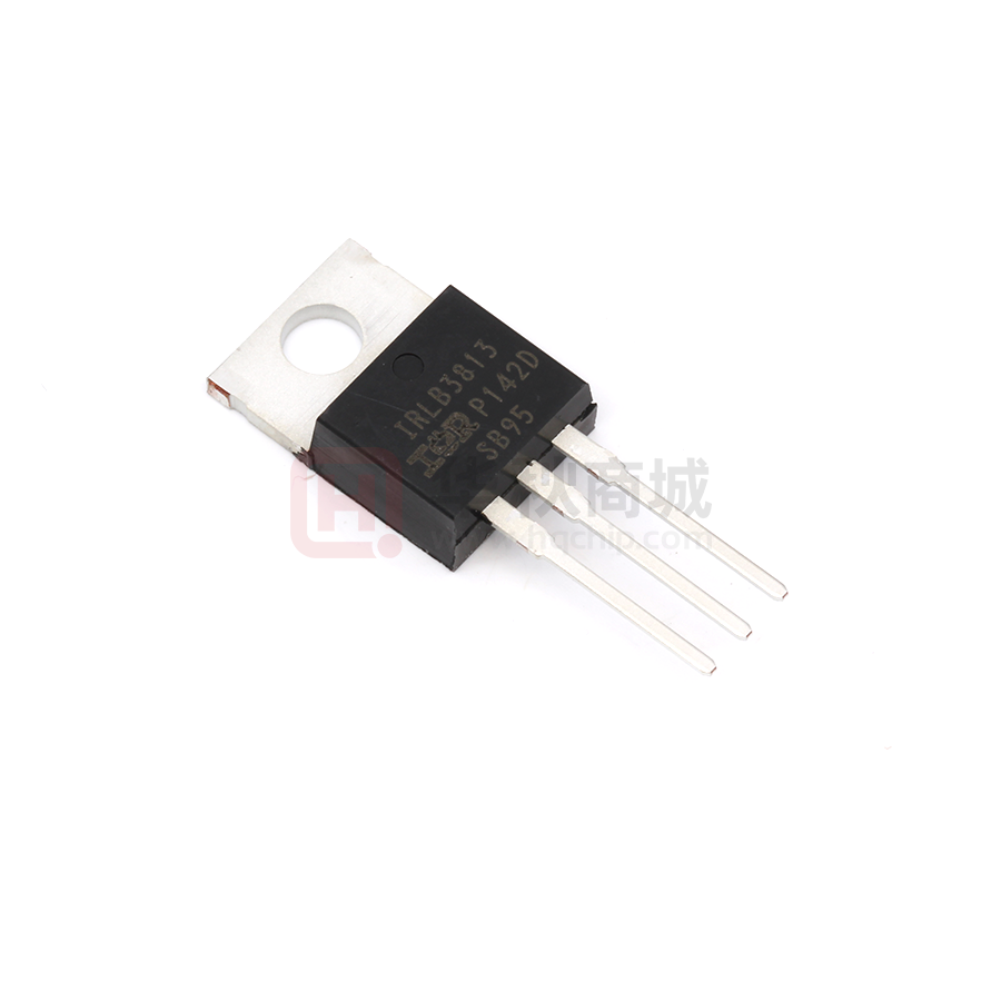
TO-220AB
G
D
S
Gate
Drain
Source
Absolute Maximum Ratings
Parameter
Max.
VDS
Drain-to-Source Voltage
30
VGS
± 20
ID @ TC = 25°C
Gate-to-Source Voltage
Continuous Drain Current, VGS @ 10V
260
ID @ TC = 100°C
Continuous Drain Current, VGS @ 10V
190
IDM
Pulsed Drain Current
1050
c
PD @TC = 25°C
Maximum Power Dissipation
PD @TC = 100°C
Maximum Power Dissipation
Linear Derating Factor
TJ
TSTG
Soldering Temperature, for 10 seconds
Mounting torque, 6-32 or M3 screw
V
h
h
g
g
Operating Junction and
Storage Temperature Range
Units
A
230
W
120
1.6
W/°C
-55 to + 175
300 (1.6mm from case)
10lb in (1.1N m)
x
°C
x
Thermal Resistance
Typ.
Max.
–––
0.64
Case-to-Sink, Flat Greased Surface
0.50
–––
Junction-to-Ambient
–––
62
RθJC
Junction-to-Case
RθCS
RθJA
Parameter
g
f
Units
°C/W
Notes through are on page 9
www.irf.com
1
07/03/09
�IRLB3813PbF
Static @ TJ = 25°C (unless otherwise specified)
Parameter
BVDSS
∆ΒVDSS/∆TJ
Min. Typ. Max. Units
30
–––
–––
Breakdown Voltage Temp. Coefficient
Static Drain-to-Source On-Resistance
–––
–––
11
1.60
––– mV/°C Reference to 25°C, ID = 1.0mA
mΩ VGS = 10V, ID = 60A
1.95
Gate Threshold Voltage
–––
1.35
2.00
1.90
2.60
2.35
IDSS
Gate Threshold Voltage Coefficient
Drain-to-Source Leakage Current
–––
–––
-7.8
–––
–––
1.0
IGSS
Gate-to-Source Forward Leakage
–––
–––
–––
–––
100
100
nA
VDS = 24V, VGS = 0V, TJ = 125°C
VGS = 20V
Gate-to-Source Reverse Leakage
Forward Transconductance
–––
140
–––
–––
-100
–––
S
VGS = -20V
VDS = 15V, ID = 48A
Total Gate Charge
Pre-Vth Gate-to-Source Charge
–––
–––
57
16
86
–––
Post-Vth Gate-to-Source Charge
Gate-to-Drain Charge
–––
–––
6.7
19
–––
–––
Qgodr
Qsw
Gate Charge Overdrive
Switch Charge (Qgs2 + Qgd)
–––
–––
15
25.7
–––
–––
Qoss
RG
Output Charge
Gate Resistance
–––
–––
35
0.87
–––
1.3
nC
Ω
td(on)
tr
Turn-On Delay Time
Rise Time
–––
–––
36
170
–––
–––
ns
td(off)
tf
Turn-Off Delay Time
Fall Time
–––
–––
33
60
–––
–––
Ciss
Coss
Input Capacitance
Output Capacitance
–––
–––
8420
1620
–––
–––
Crss
Reverse Transfer Capacitance
–––
650
–––
RDS(on)
VGS(th)
∆VGS(th)/∆TJ
gfs
Qg
Qgs1
Qgs2
Qgd
V
Conditions
Drain-to-Source Breakdown Voltage
V
VGS = 0V, ID = 250µA
e
e
VGS = 4.5V, ID = 48A
VDS = VGS, ID = 150µA
mV/°C
µA VDS = 24V, VGS = 0V
VDS = 15V
nC
VGS = 4.5V
ID = 48A
See Fig. 16
VDS = 16V, VGS = 0V
VDD = 15V, VGS = 4.5V
ID = 48A
e
RG = 1.8Ω
pF
See Fig. 14
VGS = 0V
VDS = 15V
ƒ = 1.0MHz
Avalanche Characteristics
EAS
Parameter
Single Pulse Avalanche Energy
IAR
Avalanche Current
�c
d
Typ.
–––
Max.
520
Units
mJ
–––
48
A
Diode Characteristics
Parameter
Min. Typ. Max. Units
h
IS
Continuous Source Current
–––
–––
260
ISM
(Body Diode)
Pulsed Source Current
–––
–––
1050
VSD
trr
(Body Diode)
Diode Forward Voltage
Reverse Recovery Time
–––
–––
–––
24
1.0
36
V
ns
Qrr
Reverse Recovery Charge
–––
22
33
nC
2
�c
Conditions
MOSFET symbol
A
showing the
integral reverse
p-n junction diode.
TJ = 25°C, IS = 48A, VGS = 0V
TJ = 25°C, IF = 48A, VDD = 15V
di/dt = 244A/µs
e
e
www.irf.com
�IRLB3813PbF
10000
1000
1000
BOTTOM
TOP
ID, Drain-to-Source Current (A)
ID, Drain-to-Source Current (A)
TOP
VGS
10V
9.0V
7.0V
5.5V
4.5V
4.0V
3.5V
3.0V
BOTTOM
VGS
10V
9.0V
7.0V
5.5V
4.5V
4.0V
3.5V
3.0V
100
100
≤60µs PULSE WIDTH
Tj = 25°C
3.0V
≤60µs PULSE WIDTH
3.0V
Tj = 175°C
10
10
0.1
1
10
100
0.1
V DS, Drain-to-Source Voltage (V)
10
100
V DS, Drain-to-Source Voltage (V)
Fig 1. Typical Output Characteristics
Fig 2. Typical Output Characteristics
1000
2.0
RDS(on) , Drain-to-Source On Resistance
(Normalized)
ID, Drain-to-Source Current (A)
1
T J = 175°C
100
T J = 25°C
10
1
VDS = 15V
≤60µs PULSE WIDTH
0.1
ID = 120A
VGS = 10V
1.5
1.0
0.5
1
2
3
4
5
6
VGS, Gate-to-Source Voltage (V)
Fig 3. Typical Transfer Characteristics
www.irf.com
7
-60 -40 -20 0 20 40 60 80 100120140160180
T J , Junction Temperature (°C)
Fig 4. Normalized On-Resistance
vs. Temperature
3
�IRLB3813PbF
100000
14.0
VGS = 0V,
f = 1 MHZ
C iss = C gs + C gd, C ds SHORTED
C rss = C gd
VGS, Gate-to-Source Voltage (V)
ID= 48A
C, Capacitance (pF)
C oss = C ds + C gd
10000
Ciss
Coss
1000
Crss
100
12.0
VDS= 24V
VDS= 15V
10.0
8.0
6.0
4.0
2.0
0.0
1
10
100
0
VDS, Drain-to-Source Voltage (V)
75
100
125
150
Fig 6. Typical Gate Charge vs.
Gate-to-Source Voltage
10000
1000
T J = 175°C
ID, Drain-to-Source Current (A)
ISD, Reverse Drain Current (A)
50
QG, Total Gate Charge (nC)
Fig 5. Typical Capacitance vs.
Drain-to-Source Voltage
100
TJ = 25°C
10
1
OPERATION IN THIS AREA
LIMITED BY R DS(on)
1000
100µsec
1msec
100
10msec
10
Tc = 25°C
Tj = 175°C
Single Pulse
VGS = 0V
1
0.1
0.0
0.5
1.0
1.5
2.0
2.5
VSD, Source-to-Drain Voltage (V)
Fig 7. Typical Source-Drain Diode
Forward Voltage
4
25
3.0
0
1
10
100
VDS, Drain-to-Source Voltage (V)
Fig 8. Maximum Safe Operating Area
www.irf.com
�IRLB3813PbF
3.0
Limited By Package
250
ID, Drain Current (A)
VGS(th) , Gate threshold Voltage (V)
300
200
150
100
50
2.5
2.0
1.5
ID = 150µA
ID = 1.0mA
1.0
ID = 1.0A
0.5
0.0
0
25
50
75
100
125
150
-75 -50 -25 0
175
25 50 75 100 125 150 175 200
TJ , Temperature ( °C )
T C , Case Temperature (°C)
Fig 10. Threshold Voltage vs. Temperature
Fig 9. Maximum Drain Current vs.
Case Temperature
Thermal Response ( Z thJC ) °C/W
1
D = 0.50
0.20
0.10
0.05
0.1
0.02
0.01
0.01
0.001
τJ
R1
R1
τJ
τ1
1E-005
R3
R3
Ri (°C/W)
R4
R4
τC
τ
τ1
τ2
τ2
τ3
τ3
Ci= τi/Ri
Ci i/Ri
SINGLE PULSE
( THERMAL RESPONSE )
0.0001
1E-006
R2
R2
τ4
τ4
τi (sec)
0.4985
0.004600
0.0022
8.246580
0.0001
6.149340
0.1392
0.000300
Notes:
1. Duty Factor D = t1/t2
2. Peak Tj = P dm x Zthjc + Tc
0.0001
0.001
0.01
0.1
t1 , Rectangular Pulse Duration (sec)
Fig 11. Maximum Effective Transient Thermal Impedance, Junction-to-Case
www.irf.com
5
�12
2200
EAS , Single Pulse Avalanche Energy (mJ)
RDS(on), Drain-to -Source On Resistance (m Ω)
IRLB3813PbF
ID = 60A
10
8
6
T J = 125°C
4
2
TJ = 25°C
0
ID
TOP
17A
27A
BOTTOM 48A
2000
1800
1600
1400
1200
1000
800
600
400
200
0
2
4
6
8
10
25
50
75
100
125
150
175
Starting T J , Junction Temperature (°C)
VGS, Gate -to -Source Voltage (V)
Fig 12. On-Resistance vs. Gate Voltage
Fig 13a. Maximum Avalanche Energy
vs. Drain Current
V(BR)DSS
15V
L
VDS
DRIVER
D.U.T
RG
20V
VGS
tp
+
V
- DD
IAS
A
0.01Ω
tp
I AS
Fig 13b. Unclamped Inductive Test Circuit
VDS
VGS
RG
RD
VDS
90%
D.U.T.
+
-V DD
V GS
Pulse Width ≤ 1 µs
Duty Factor ≤ 0.1 %
Fig 14a. Switching Time Test Circuit
6
Fig 13c. Unclamped Inductive Waveforms
10%
VGS
td(on)
tr
t d(off)
tf
Fig 14b. Switching Time Waveforms
www.irf.com
�IRLB3813PbF
D.U.T
Driver Gate Drive
P.W.
+
+
-
-
*
D.U.T. ISD Waveform
Reverse
Recovery
Current
+
RG
•
•
•
•
dv/dt controlled by RG
Driver same type as D.U.T.
I SD controlled by Duty Factor "D"
D.U.T. - Device Under Test
V DD
P.W.
Period
VGS=10V
Circuit Layout Considerations
• Low Stray Inductance
• Ground Plane
• Low Leakage Inductance
Current Transformer
D=
Period
+
Body Diode Forward
Current
di/dt
D.U.T. VDS Waveform
Diode Recovery
dv/dt
Re-Applied
Voltage
Body Diode
VDD
Forward Drop
Inductor Curent
-
ISD
Ripple ≤ 5%
* VGS = 5V for Logic Level Devices
Fig 15. Peak Diode Recovery dv/dt Test Circuit for N-Channel
HEXFET® Power MOSFETs
Current Regulator
Same Type as D.U.T.
Id
Vds
50KΩ
12V
Vgs
.2µF
.3µF
D.U.T.
+
V
- DS
Vgs(th)
VGS
3mA
IG
ID
Qgodr
Qgd
Qgs2 Qgs1
Current Sampling Resistors
Fig 16a. Gate Charge Test Circuit
www.irf.com
Fig 16b. Gate Charge Waveform
7
�IRLB3813PbF
TO-220AB Package Outline (Dimensions are shown in millimeters (inches))
TO-220AB packages are not recommended for Surface Mount Application.
Note: For the most current drawing please refer to IR website at: http://www.irf.com/package/
8
www.irf.com
�IRLB3813PbF
TO-220AB Part Marking Information
(;$03/(�
7+,6�,6�$1�,5)�����
/27�&2'(�����
,17(51$7,21$/
$66(0%/('�21�::���������
,1�7+(�$66(0%/


 工商网监
湘ICP备2023018690号
工商网监
湘ICP备2023018690号

