PTMA080152M
Wideband RF LDMOS Integrated Power Amplifier
15 W, 28 V, 700 – 1000 MHz
Description
The PTMA080152M is a wideband, on chip–matched, 15-watt,
2-stage LDMOS integrated power amplifier intended for wideband
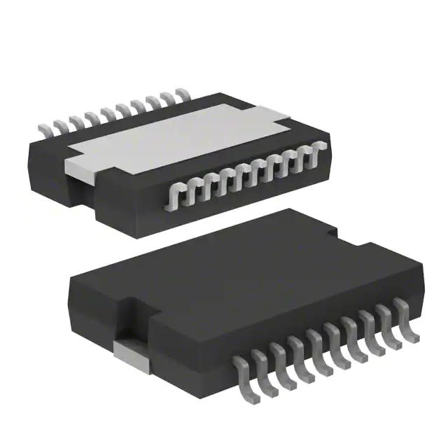
driver applications in the 700 to 1000 MHz frequency range. It is offered in a 20-lead thermally-enhanced overmolded package for cool
and reliable operation.
Features
Two-tone Drive-up
VDD = 28 V, IDQ1 = 70 mA, IDQ2 = 90 mA
ƒ = 920, 940, 960 MHz
50
•
Broadband on-chip matching, 50-ohm input and
~10-ohm output
•
Typical GSM/EDGE performance at 28 V, 920 to
960 MHz
- Gain = 30 dB
- Efficiency = 34% at 8 W output power
- EVM @ 8 W = 1.5%
- ACPR @ 400 kHz = –61 dBc
- ACPR @ 600 kHz = –75 dBc
•
Typical CW performance, 940 MHz, 28 V
- Output power at P1dB = 20 W
- Efficiency = 49%
•
Integrated ESD protection. Meets HBM Class 1B
(minimum), per JESD22-A114F.
-55
•
Excellent thermal stability, low HCI drift
-60
•
Capable of handling 10:1 VSWR @ 28 V, 20 W
(CW) output power
•
RoHS-compliant package
-10
45
-15
PAE
40
-20
35
-25
30
-30
25
-35
IMD3
-40
40
20
15
-45
920 MHz
940 MHz
10
5
-50
0
27
29
31
33
35
37
39
41
IMD
D3 (dBc)
Power Adde
ed Efficiency (%)
PTMA080152M
Package PG-DSO-20-63
43
Average Output Power ( dBm )
RF Characteristics
GSM/EDGE Characteristics (not subject to production test—verified by design/characterization in Infineon test fixture)
VDD = 28 V, IDQ1 = 70 mA, IDQ2 = 120 mA, ƒ = 920 to 960 MHz, POUT = 8 W Avg.
Characteristic
Symbol
Min
Typ
Max
Unit
Input Return Loss
IRL
—
–15
—
dB
Gain
Gps
—
30
—
dB
Power Added Efficiency
PAE
—
34
—
%
Error Vector Magnitude
EVM (RMS)
—
1.5
—
%
table continued next page
All published data at TCASE = 25°C unless otherwise indicated
ESD: Electrostatic discharge sensitive device—observe handling precautions!
Data Sheet
1 of 11
Rev. 07, 2014-05-07
�PTMA080152M
RF Characteristics (cont.)
GSM/EDGE Characteristics (cont.)
VDD = 28 V, IDQ1 = 70 mA, IDQ2 = 120 mA, ƒ = 920 to 960 MHz, POUT = 8 W Avg.
Characteristic
Modulation Spectrum
Symbol
Min
Typ
Max
Unit
400 kHz offset
ACPR1
—
–61
—
dBc
600 kHz offset
ACPR2
—
–75
—
dBc
Spurs Load 3:1
—
—
—
–60
dBc
Gain Flatness
ΔG
—
0.2
—
dB
Two-tone Measurements (tested in Infineon test fixture)
VDD = 28 V, IDQ1 = 70 mA, IDQ2 = 90 mA, POUT = 8 W avg., ƒ = 940 MHz, tone spacing = 1 MHz
Characteristic
Symbol
Min
Typ
Max
Unit
Gain
Gps
29
30
—
dB
Drain Efficiency
ηD
32.5
33.5
—
%
IMD3
—
–34
–31
dBc
Symbol
Min
Typ
Max
Unit
Third Order Intermodulation Distortion
DC Characteristics
Stage 1 Characteristics
Conditions
Drain Leakage Current
VDS = 28 V, VGS = 0 V
IDSS
—
—
1.0
µA
VDS = 63 V, VGS = 0 V
IDSS
—
—
10.0
µA
Gate Leakage Current
VGS = 10 V, VDS = 0 V
IGSS
—
—
1.0
µA
On-state Resistance
VGS = 10 V, VDS = 0.1 V
RDS(on)
—
3.48
—
Ω
Operating Gate Voltage
VDS = 28 V, IDQ1 = 70 mA,
VGS
2.0
2.5
3.0
V
Stage 2 Characteristics
Conditions
Symbol
Min
Typ
Max
Unit
Drain-source Breakdown Voltage
VGS = 0 V, IDS = 10 mA
V(BR)DSS
65
—
—
V
Drain Leakage Current
VDS = 28 V, VGS = 0 V
IDSS
—
—
1.0
µA
VDS = 63 V, VGS = 0 V
IDSS
—
—
10.0
µA
Gate Leakage Current
VGS = 10 V, VDS = 0 V
IGSS
—
—
1.0
µA
On-state Resistance
VGS = 10 V, VDS = 0.1 V
RDS(on)
—
0.6
—
Ω
Operating Gate Voltage
VDS = 28 V, IDQ2 = 90 mA
VGS
2.0
—
3.0
V
Data Sheet
2 of 11
Rev. 07, 2014-05-07
�PTMA080152M
Maximum Ratings
Parameter
Symbol
Value
Unit
Drain-Source Voltage
VDSS
65
V
Gate-Source Voltage
VGS
–0.5 to +12
V
Junction Temperature
TJ
200
°C
Input Power
PIN
15
dBm
Total Device Dissipation
PD
91
W
0.52
W/°C
TSTG
–40 to +150
°C
Stage 1
RθJC
8.5
°C/W
Stage 2
RθJ0C
2.5
°C/W
Above 25°C derate by
Storage Temperature Range
Overall Thermal Resistance (TCASE = 70°C)
POUT = 15 W, IDQ1 = 70 mA, IDQ2 = 90 mA
Moisture Sensitivity Level
Level
Test Standard
Package Temperature
Unit
3
IPC/JEDEC J-STD-020
260
°C
Ordering Information
Type and Version
Order Code
Package and Description
Shipping
PTMA080152M V1
PTMA080152MV1AUMA1
PG-DSO-20-63, molded plastic
Tape & Reel, 250 pcs
PTMA080152M V1 R500
PTMA080152MV1R500AUMA1
PG-DSO-20-63, molded plastic
Tape & Reel, 500 pcs
Data Sheet
3 of 11
Rev. 07, 2014-05-07
�PTMA080152M
Typical Performance (data taken in Infineon production test fixture)
CW Performance
Broadband Performance
VDD = 28 V
V, IDQ1 = 70 mA,
mA IDQ2 = 90 mA
ƒ = 920 , 940, 960 MHz
VDD = 28 V, IDQ1 = 70 mA, IDQ2 = 90 mA,
fixture tuned for 920 – 960 MHz
32
60
28
55
50
24
45
920 MHz
940 MHz
960 MHz
22
20
40
35
30
18
16
25
PAE
14
20
12
15
10
10
29
31
33
35
37
39
41
43
-4
Gain
24
-8
20
-12
16
-16
12
-20
Return Loss
8
-24
4
-28
0
-32
750
45
800
850
900
950 1000 1050 1100 1150
Frequency (MHz)
Output Power (dBm)
EDGE - EVM
EDGE - EVM
VDD = 28 V, IDQ1 = 70 mA, IDQ2 = 120 mA,
q
series are at selected frequencies
VDD = 28 V, IDQ1 = 70 mA, IDQ2 = 120 mA,
ƒ = 942.6 MHz
50
90 °C
–25 °C
25 °C
45
40
9
8
35
7
30
6
25
5
20
4
PAE
15
EVM
10
5
3
2
1
0
Powerr Added Effficiency (%))
10
Error Vector
V
Magnitude (%)
Power Added Efficiency (%)
50
45
40
9
8
35
7
30
EVM
25
20
6
5
4
PAE
15
3
10
2
5
1
0
0
0
30 31 32 33 34 35 36 37 38 39 40 41 42
30 31 32 33 34 35 36 37 38 39 40 41 42
Output Power (dBm)
Output Power (dBm)
Data Sheet
10
925.2 MHz
942 6 MH
942.6
MHz
959.8 MHz
Error V
Vector Mag
gnitude (%))
Gain ((dB)
26
Gain (dB)
Gain
28
0
Retturn Loss (dB)
65
30
Power Added E
Efficiency(%)
32
4 of 11
Rev. 07, 2014-05-07
�PTMA080152M
Typical Performance (cont.)
EDGE Modulation Spectrum Performance
EDGE Modulation Spectrum Performance
VDD = 28 V
V, IDQ1 = 70 mA
mA, IDQ2 = 120 mA
mA,
series show ƒ = 942.6 MHz, at selected temperatures
VDD = 28 V, IDQ1 = 70 mA, IDQ2 = 120 mA,
series are at selected frequencies
-35
-45
30
-55
20
-65
400 kHz
10
-75
600 kH
kHz
0
30
32
34
36
38
-40
925.2 MHz
942.6 MHz
959.8 MHz
40
35
PAE
-45
-50
30
-55
25
-60
20
-65
400 kHz
15
-70
-75
75
10
5
-80
600 kHz
0
-85
40
-35
45
-85
30
42
Mod
dulation Spectrum (dBc)
40
PAE
Powe
er Added Efficiency (%)
50
90 °C
–25 °C
25 °C
Modulatio
on Spectrum (dBc)
Power Add
P
ded Efficie
ency (%)
50
32
34
36
38
40
42
Output Power (dBm)
Output Power (dBm)
Gate – Source Voltage vs. Temperature
Norm
malized G
Gate – So
ource Volttage
(th
hreshold), V
VDD = 28 V, IDQ1 = 70 mA, IDQ2 = 90 mA
1.15
VGS1
VGS2
1.10
1.05
Slope = –1.3 mV/°C
1.00
09
0.95
0.90
0.85
-30
-10
10
30
50
70
90
T
t
Temperature
(°C)
Data Sheet
5 of 11
Rev. 07, 2014-05-07
�PTMA080152M
Broadband Circuit Impedance
Z Load Ω
740
9.8
–3.1
760
9.5
–2.4
780
9.2
–1.8
800
9.0
–1.2
820
8.8
–0.5
840
8.7
0.1
860
8.6
0.8
880
8.5
1.4
900
8.5
2.1
920
8.5
2.8
940
8.5
3.5
960
8.6
4.3
980
8.7
5.0
1000
8.8
5.8
Z0 = 50 Ω
1. 0
1000 MHz
Z Load
0.4
–3.7
0.3
10.1
0.2
720
0.1
–4.3
0.0
10.6
NER
700
A
jX
LOAD S T OW ARD
NGTH
R
RD GE
MHz
- W A V E LE NGTH
S T OW
A
Frequency
700 MHz
0.1
See next page for reference circuit information
Data Sheet
6 of 11
Rev. 07, 2014-05-07
�PTMA080152M
Reference Circuit
VD1
C1
100μF
50V
C2
10μF
C3
1μF
C4
0.1μF
C5
47pF
VD2
C15
47 pF
DUT
J1
2
1
C7
10μF
R1
0
C9
0.1μF
C8
1μF
19
3
18
4
17
PTMA080152M
16
6
15
14
8
13
9
12
10
11
VG1
R3
2k
20
2
7
C6
1pF
variable
1
C16
0.1μF
C17
1μF
18
10μF
C19
100μF
50V
4
3
C22
33pF
5
6
8
7
J2
C21
5.6pF
C20
2.2pF
C10
47pF
Q1
V G2
R4
2k
a 080152 m_ bd_ 8-22-11
variable
C11
10μF
R2
0
C12
1μF
C13
0.1μF
C14
47pF
Q2
Reference circuit schematic for ƒ = 940 MHz
Circuit Assembly Information
DUT
PTMA080152M, LDMOS IC
Reference Fixture Part No. LTN/PTMA080152M
PCB
0.76 mm [.030"] thick, εr = 3.48, Rogers RO4350, 1 oz. copper
Find Gerber files for this reference fixture on the Infineon Web site at (http://www.infineon.com/rfpower)
Microstrip
Electrical Characteristics at 940 MHz1
L x W (mm)
L x W (in.)
1
0.017 λ, 50.0 Ω
3.00 x 1.70
0.118 x 0.067
2
0.143 λ, 50.0 Ω
24.71 x 1.70
0.973 x 0.067
3
0.024 λ, 10.6 Ω
4.09 x 12.70
0.161 x 0.500
4
0.144 λ, 59.0 Ω
24.77 x 1.30
0.975 x 0.051
5
0.044 λ, 34.0 Ω
7.57 x 3.02
0.298 x 0.119
6
0.044 λ, 44.0 Ω
8.33 x 2.11
0.328 x 0.083
7
0.0702 λ, 44.0 Ω
12.12 x 2.11
0.477 x 0.083
8
0.030 λ, 44.0 Ω
5.18 x 2.11
0.204 x 0.083
Data Sheet
7 of 11
Rev. 07, 2014-05-07
�PTMA080152M
Reference Circuit (cont.)
VD 2
VD 1
C15
C16
C17 C18
C1
C19
C2
C3
C4
C5
C22
RF_IN
RF_OUT
C10
C9
C8
C6
C21
V G1
C20
C14
C13
C12
C11
C7
R3
V G2
R4
R1
Q1
Q2
R2
a 0 8 0 1 5m2_cd _ 2- 1 0- 0 9
Reference circuit assembly diagram (not to scale)
Component
Description
Suggested Manufacturer
C3, C8, C12, C17
Ceramic capacitor, 1 µF
Digi-Key
P/N or Comment
445-1411-2-ND
C4, C9, C13, C16
Capacitor, 0.1 µF
Digi-Key
PCC104BCT-ND
C2, C7, C11, C18
Tantalum capacitor, 10 µF, 50 V
Digi-Key
P5571-ND
C1, C19
Electrolytic capacitor, 100 µF, 50 V
Digi-Key
PCE3718CT-ND
C6
Ceramic capacitor, 1.0 pF
ATC
600S 1RO CT
C20
Ceramic capacitor, 2.2 pF
ATC
600S 2R2 CT
C21
Ceramic capacitor, 5.6 pF
ATC
600S 5R6 CT
C22
Ceramic capacitor, 33 pF
ATC
600S 330 JT
C5, C10, C14, C15
Ceramic capacitor, 47 pF
ATC
600S 470 JT
Q1, Q2
Transistor
Infineon Technologies
BCP56
R1, R2
Chip resistor, 0 ohms
Digi-Key
PXXECT-ND
R3, R4
Variable resistor, 2K ohms
Digi-Key
3224W-202ETR-ND
Data Sheet
8 of 11
Rev. 07, 2014-05-07
�PTMA080152M
Pinout Diagram (top view)
VDD 1
1
20
NC
VDD 1
2
19
NC
NC
3
18
VDD 2, RF Out
NC
4
17
VDD 2, RF Out
RF In
5
16
VDD 2, RF Out
RF In
6
15
VDD 2, RF Out
VG 1
7
14
VDD 2, RF Out
VG 2
8
13
VDD 2, RF Out
NC
9
12
NC
NC
10
11
NC
a 0 8 0 1 5
m2
_ p d _
1 0 -3 1 -0 8
Source/ground: plated copper heatslug on backside of package
(Find the latest and most complete information about products and packaging at the Infineon Internet page
(http://www.infineon.com/rfpower)
Data Sheet
9 of 11
Rev. 07, 2014-05-07
�PTMA080152M
Package Outline Specifications
Package PG-DSO-20-63
��
�����
�>�����@�0$;
,1'(;�3,1��
�
��
�;�����
�>�����@�0$;
���3/6�
���������
>����������@
���� ��
����
�>�����@ �>�����@
�����
�>�����@
��
��
��;������ ������
��;������ �����
723�9,(:
%27720�9,(:
����
�>�����@�0$;�
���3/6�
��
�������3/6�
723�%27720
$//�6,'(6
���������
�>����������@��
6((�'(7$,/�$
�����
>�����@�0$;
����
�>�����@
�
���������
>����������@
���������
>�����������@
��
(1'�9,(:
����PP 0 & $ 6 % 6
6,'(�9,(:
����
�>�����@
*$8*(�3/$1(
����
�>�����@�5()
���������
²����
������
�>���������������@
²�����
3*�'62������B�SRB��B����������
�����
>�������@
67$1'2))
�
��������
>����������@
����
�>�����@�5()
'(7$,/�$�
Diagram Notes—unless otherwise specified:
1. Interpret dimensions and tolerances per ASME Y14.5M-1994.
2. Package dimensions: 11.0 mm by 15.9 mm by 3.35 mm.
3. JEDEC drawing number: MO-166.
4. Does not include plastic or metal protrusion of 0.15 mm max per side.
5. Does not include dambar protrusion; maximum allowable dambar
protrusion shall be 0.08 mm.
6. Bottom metallization.
7. Sn plating (matte): 5 – 15 micron [196.85 – 590.55 microinch].
Refer to Application Note “Recommendations for Printed Circuit Board Assembly of Infineon DSO and SSOP Packages” for
additional information.
Data Sheet
10 of 11
Rev. 07, 2014-05-07
�PTMA080152M V1
Revision History
Revision
Date
Data Sheet
Page
Subjects (major changes since last revision)
01
2007-05-05
Preliminary
all
Preliminary specification for new product in development.
02
2009-02-27
Production
all
Revise package information and circuit diagrams, add impedance information.
03
2009-08-31
Production
1
Revise VSWR rating.
04
2010-04-16
Production
3; 10
Add moisture sensitivity information; update package outline notes.
05
2011-05-17
Production
2; 4
Revise DC table; remove graph.
06
2011-08-22
Production
2; all
Revise two-tone table; minor updates to graphics and diagrams for readability.
07
2014-05-07
Production
3
Add shipping option.
We Listen to Your Comments
Any information within this document that you feel is wrong, unclear or missing at all?
Your feedback will help us to continuously improve the quality of this document.
Please send your proposal (including a reference to this document) to:
(highpowerRF@infineon.com)
To request other information, contact us at:
+1 877 465 3667 (1-877-GO-LDMOS) USA
or +1 408 776 0600 International
Edition 2014-05-07
Published by
Infineon Technologies AG
85579 Neubiberg, Germany
© 2012 Infineon Technologies AG
All Rights Reserved.
Legal Disclaimer
The information given in this document shall in no event be regarded as a guarantee of conditions or characteristics.
With respect to any examples or hints given herein, any typical values stated herein and/or any information regarding the
application of the device, Infineon Technologies hereby disclaims any and all warranties and liabilities of any kind,
including without limitation, warranties of non-infringement of intellectual property rights of any third party.
Information
For further information on technology, delivery terms and conditions and prices, please contact the nearest
Infineon Technologies Office (www.infineon.com/rfpower).
Warnings
Due to technical requirements, components may contain dangerous substances. For information on the types in question,
please contact the nearest Infineon Technologies Office.
Infineon Technologies components may be used in life-support devices or systems only with the express written approval of Infineon Technologies, if a failure of such components can reasonably be expected to cause the failure of that life-support device
or system or to affect the safety or effectiveness of that device or system. Life support devices or systems are intended to be
implanted in the human body or to support and/or maintain and sustain and/or protect human life. If they fail, it is
reasonable to assume that the health of the user or other persons may be endangered.
Data Sheet
11 of 10
Rev. 07, 2014-05-07
�