SPP17N80C3
SPA17N80C3
Cool MOS™ Power Transistor
Feature
VDS
800
V
RDS(on)
0.29
Ω
ID
17
A
• New revolutionary high voltage technology
• Worldwide best RDS(on) in TO 220
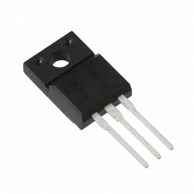
PG-TO220-3-31 PG-TO220
• Ultra low gate charge
• Periodic avalanche rated
• Extreme dv/dt rated
1
• Ultra low effective capacitances
2
3
P-TO220-3-31
• Improved transconductance
• PG-TO-220-3-31: Fully isolated package (2500 VAC; 1 minute)
Type
Package
Ordering Code
Marking
SPP17N80C3
PG-TO220
Q67040-S4353
17N80C3
SPA17N80C3
PG-TO220-3-31 SP000216353
17N80C3
Maximum Ratings
Parameter
Symbol
Value
SPP
Continuous drain current
Unit
SPA
A
ID
TC = 25 °C
17
17 1)
TC = 100 °C
11
11 1)
51
51
Pulsed drain current, tp limited by Tjmax
ID puls
A
Avalanche energy, single pulse
EAS
670
670
EAR
0.5
0.5
Avalanche current, repetitive tAR limited by Tjmax
IAR
17
17
A
Gate source voltage
VGS
±20
±20
V
Gate source voltage AC (f >1Hz)
VGS
±30
±30
Power dissipation, TC = 25°C
Ptot
208
42
Operating and storage temperature
Tj , Tstg
mJ
ID=3.4A, VDD=50V
Avalanche energy, repetitive tAR limited by Tjmax2)
ID=17A, VDD=50V
Rev. 2.7
Final Data Sheet
Page 1
1
-55...+150
W
°C
2011-09-27
Rev. 2.8, 2017-07-25
�SPP17N80C3
SPA17N80C3
Maximum Ratings
Parameter
Symbol
Drain Source voltage slope
dv/dt
Value
Unit
50
V/ns
Values
Unit
VDS = 640 V, ID = 17 A, Tj = 125 °C
Thermal Characteristics
Parameter
Symbol
min.
typ.
max.
Thermal resistance, junction - case
RthJC
-
-
0.6
Thermal resistance, junction - case, FullPAK
RthJC_FP
-
-
3.6
Thermal resistance, junction - ambient, leaded
RthJA
-
-
62
Thermal resistance, junction - ambient, FullPAK
RthJA_FP
-
-
80
SMD version, device on PCB:
RthJA
@ min. footprint
-
-
62
@ 6 cm 2 cooling area 3)
-
35
-
-
-
260
Soldering temperature, wavesoldering
Tsold
K/W
°C
1.6 mm (0.063 in.) from case for 10s 4)
Electrical Characteristics, at Tj=25°C unless otherwise specified
Parameter
Symbol
Conditions
Drain-source breakdown voltage V(BR)DSS VGS=0V, ID=0.25mA
Drain-Source avalanche
V(BR)DS VGS=0V, ID=17A
Values
Unit
min.
typ.
max.
800
-
-
-
870
-
2.1
3
3.9
V
breakdown voltage
Gate threshold voltage
VGS(th)
ID=1000µA, VGS=VDS
Zero gate voltage drain current
I DSS
VDS=800V, V GS=0V,
Gate-source leakage current
I GSS
Drain-source on-state resistance RDS(on)
Gate input resistance
Rev. 2.7
Final Data Sheet
RG
µA
Tj=25°C
-
0.5
25
Tj=150°C
-
-
250
VGS=20V, V DS=0V
-
-
100
VGS=10V, ID=11A
Ω
Tj=25°C
-
0.25
0.29
Tj=150°C
-
0.78
-
f=1MHz, open drain
-
0.7
-
Page 2
2
nA
2011-09-27
Rev. 2.8, 2017-07-25
�SPP17N80C3
SPA17N80C3
Electrical Characteristics
Parameter
Transconductance
Symbol
gfs
Conditions
VDS≥2*ID*R DS(on)max,
Values
Unit
min.
typ.
max.
-
15
-
S
pF
ID=11A
Input capacitance
Ciss
VGS=0V, VDS=25V,
-
2320
-
Output capacitance
Coss
f=1MHz
-
1250
-
Reverse transfer capacitance
Crss
-
60
-
-
59
-
-
124
-
Effective output capacitance,5) Co(er)
VGS=0V,
energy related
VDS=0V to 480V
Effective output capacitance,6) Co(tr)
time related
Turn-on delay time
td(on)
VDD=400V, VGS=0/10V,
-
25
-
Rise time
tr
ID=17A,
-
15
-
Turn-off delay time
td(off)
RG =4.7Ω, Tj =125°C
-
72
82
Fall time
tf
-
6
9
-
12
-
-
46
-
-
91
177
-
6
-
ns
Gate Charge Characteristics
Gate to source charge
Qgs
Gate to drain charge
Qgd
Gate charge total
Qg
VDD=640V, ID=17A
VDD=640V, ID=17A,
nC
VGS=0 to 10V
Gate plateau voltage
V(plateau) VDD=640V, ID=17A
V
1Limited only by maximum temperature
2Repetitve avalanche causes additional power losses that can be calculated as P =E *f.
AR
AV
3Device on 40mm*40mm*1.5mm epoxy PCB FR4 with 6cm² (one layer, 70 µm thick) copper area for drain
connection. PCB is vertical without blown air.
4Soldering temperature for TO-263: 220°C, reflow
5C
o(er)
is a fixed capacitance that gives the same stored energy as Coss while VDS is rising from 0 to 80% VDSS.
6C
o(tr)
is a fixed capacitance that gives the same charging time as Coss while VDS is rising from 0 to 80% VDSS.
Rev. 2.7
Final Data Sheet
Page 3
3
2011-09-27
Rev. 2.8, 2017-07-25
�SPP17N80C3
SPA17N80C3
Electrical Characteristics
Parameter
Symbol
Inverse diode continuous
IS
Conditions
Values
Unit
min.
typ.
max.
-
-
17
-
-
51
TC=25°C
A
forward current
Inverse diode direct current,
I SM
pulsed
Inverse diode forward voltage
VSD
VGS =0V, IF=IS
-
1
1.2
V
Reverse recovery time
t rr
VR =400V, IF =IS ,
-
550
-
ns
Reverse recovery charge
Q rr
diF/dt=100A/µs
-
15
-
µC
Peak reverse recovery current
I rrm
-
51
-
A
Peak rate of fall of reverse
dirr/dt
-
1200
-
A/µs
Tj=25°C
recovery current
Typical Transient Thermal Characteristics
Symbol
Value
Unit
SPP
SPA
Rth1
0.00812
0.00812
Rth2
0.016
Rth3
Symbol
Value
Unit
SPP
SPA
Cth1
0.0003562
0.0003562
0.016
Cth2
0.001337
0.001337
0.031
0.031
Cth3
0.001831
0.001831
Rth4
0.114
0.16
Cth4
0.005033
0.005033
Rth5
0.135
0.324
Cth5
0.012
0.008657
Rth6
0.059
2.522
Cth6
0.092
0.412
Tj
K/W
R th1
R th,n
T case
Ws/K
E xternal H eatsink
P tot (t)
C th1
C th2
C th,n
T am b
Rev. 2.7
Final Data Sheet
Page 4
4
2011-09-27
Rev. 2.8, 2017-07-25
�SPP17N80C3
SPA17N80C3
1 Power dissipation
2 Power dissipation FullPAK
Ptot = f (TC)
Ptot = f (TC)
240
SPP17N80C3
45
W
W
200
35
160
Ptot
Ptot
180
140
30
25
120
20
100
15
80
60
10
40
5
20
0
0
20
40
60
80
100
120
°C
0
0
160
20
40
60
80
100
120
TC
3 Safe operating area
4 Safe operating area FullPAK
ID = f ( VDS )
ID = f (VDS)
parameter : D = 0 , TC=25°C
parameter: D = 0, TC = 25°C
10
2
°C 160
TC
10 2
10 1
10 1
ID
A
ID
A
10 0
10 -1
10 -2 0
10
Rev. 2.7
Final Data Sheet
10 0
tp = 0.001 ms
tp = 0.01 ms
tp = 0.1 ms
tp = 1 ms
DC
10
1
10 -1
10
2
10
V
VDS
10 -2 0
10
3
Page 5
5
tp = 0.001 ms
tp = 0.01 ms
tp = 0.1 ms
tp = 1 ms
tp = 10 ms
DC
10
1
10
2
10
V
VDS
2011-09-27
Rev. 2.8, 2017-07-25
3
�SPP17N80C3
SPA17N80C3
5 Transient thermal impedance
6 Transient thermal impedance FullPAK
ZthJC = f (tp)
ZthJC = f (tp)
parameter: D = tp/T
parameter: D = tp/t
10 1
10 1
K/W
K/W
10 0
ZthJC
ZthJC
10 0
10 -1
D = 0.5
D = 0.2
D = 0.1
D = 0.05
D = 0.02
D = 0.01
single pulse
10 -2
10 -3
10 -4 -7
10
10
-6
10
-5
10
-4
10
-3
s
tp
10 -1
D = 0.5
D = 0.2
D = 0.1
D = 0.05
D = 0.02
D = 0.01
single pulse
10 -2
10 -3
10
10 -4 -7
-6
-5
-4
-3
-2
-1
10
10
10
10
10
10
10
-1
1
s 10
tp
7 Typ. output characteristic
8 Typ. output characteristic
ID = f (VDS); Tj =25°C
ID = f (VDS); Tj =150°C
parameter: tp = 10 µs, VGS
parameter: tp = 10 µs, VGS
35
70
A
20V
10V
60
20V
10V
8V
7V
A
55
25
45
6.5V
6V
ID
ID
50
8V
20
40
7V
35
5.5V
15
30
25
6V
5V
10
20
15
4.5V
5V
10
5
4V
5
0
0
5
10
15
20
0
0
30
VDS
V
Rev. 2.7
Final Data Sheet
5
10
15
20
30
VDS
V
Page 6
6
2011-09-27
Rev. 2.8, 2017-07-25
�SPP17N80C3
SPA17N80C3
9 Typ. drain-source on resistance
10 Drain-source on-state resistance
RDS(on)=f(ID)
RDS(on) = f (Tj)
parameter: Tj=150°C, VGS
parameter : ID = 11 A, VGS = 10 V
1.5
1.6
Ω
SPP17N80C3
Ω
RDS(on)
RDS(on)
1.3
1.2
1.1
4V 4.5V 5V
5.5V
6V
6.5V
1
1.2
1
0.8
0.9
0.6
7V
8V
10V
20V
0.8
0.7
0.4
98%
typ
0.2
0.6
0.5
0
5
10
15
20
25
0
-60
35
A
-20
20
60
°C
100
ID
180
Tj
11 Typ. transfer characteristics
12 Typ. gate charge
ID = f ( VGS ); VDS≥ 2 x ID x RDS(on)max
VGS = f (Q Gate)
parameter: ID = 17 A pulsed
parameter: tp = 10 µs
65
16
SPP17N80C3
A
V
25°C
55
50
12
VGS
ID
45
40
35
150°C
0,2 VDS max
10
0,8 VDS max
8
30
25
6
20
4
15
10
2
5
0
0
2
4
Rev. 2.7
Final Data Sheet
6
8
10
12
14
16
0
0
V 20
VGS
20
40
60
80
100
120
nC
160
QGate
Page 7
7
2011-09-27
Rev. 2.8, 2017-07-25
�SPP17N80C3
SPA17N80C3
13 Forward characteristics of body diode
14 Avalanche SOA
IF = f (VSD)
IAR = f (tAR)
parameter: Tj , tp = 10 µs
par.: Tj ≤ 150 °C
10 2
SPP17N80C3
18
A
A
14
IF
IAR
10 1
12
10
8
10 0
6
Tj = 25 °C typ
T j(START)=25°C
Tj = 150 °C typ
4
Tj = 25 °C (98%)
2
Tj = 150 °C (98%)
10 -1
0
0.4
0.8
1.2
1.6
2
2.4 V
T j(START)=125°C
0 -3
10
3
10
-2
10
-1
10
0
10
1
10
2
µs 10
tAR
VSD
15 Avalanche energy
16 Drain-source breakdown voltage
EAS = f (Tj)
V(BR)DSS = f (Tj)
4
par.: ID = 3.4 A, VDD = 50 V
980
700
mJ
V
600
940
V(BR)DSS
550
E AS
SPP17N80C3
500
450
400
920
900
880
860
350
840
300
820
250
800
200
780
150
100
760
50
740
0
25
50
75
100
720
-60
150
°C
Tj
Rev. 2.7
Final Data Sheet
-20
20
60
100
180
°C
Tj
Page 8
8
2011-09-27
Rev. 2.8, 2017-07-25
�SPP17N80C3
SPA17N80C3
17 Avalanche power losses
18 Typ. capacitances
PAR = f (f )
C = f (VDS)
parameter: EAR =0.5mJ
parameter: VGS =0V, f=1 MHz
10 5
500
pF
W
10 4
400
C
PAR
Ciss
350
300
10 3
250
10 2
200
Coss
150
Crss
10 1
100
50
0 4
10
10
5
10 0
0
6
10
Hz
f
100
200
300
400
500
600
800
V
VDS
19 Typ. Coss stored energy
Eoss=f(VDS)
18
µJ
E oss
14
12
10
8
6
4
2
0
0
100
Rev. 2.7
Final Data Sheet
200
300
400
500
600
800
V
VDS
Page 9
9
2011-09-27
Rev. 2.8, 2017-07-25
�SPP17N80C3
SPA17N80C3
Definition of diodes switching characteristics
Rev. 2.7
Final Data Sheet
Page 10
10
201109-27
Rev. 2.8, 2017-07-25
�SPP17N80C3
SPA17N80C3
PG-TO220-3-1, PG-TO220-3-21
Rev. 2.7
Final Data Sheet
Page 11
11
2011-09-27
Rev. 2.8, 2017-07-25
�SPP17N80
0C3
SPA17N80
0C3
Final Datta Sheet
Final Data Sheet
1
12
Rev. 2.2
2, 2016‐08‐0
04
Rev. 2.8, 2017-07-25
�800V�CoolMOSª�C3�Power�Transistor
SPAl7N80C3�
Revision�History
SPAl7N80C3
Revision:�2017-07-27,�Rev.�2.8
Previous Revision
Revision
Date
Subjects (major changes since last revision)
2.8
2017-07-27
Revised package drawing on page 12
Trademarks�of�Infineon�Technologies�AG
AURIX™,�C166™,�CanPAK™,�CIPOS™,�CoolGaN™,�CoolMOS™,�CoolSET™,�CoolSiC™,�CORECONTROL™,�CROSSAVE™,�DAVE™,�DI-POL™,�DrBlade™,
EasyPIM™,�EconoBRIDGE™,�EconoDUAL™,�EconoPACK™,�EconoPIM™,�EiceDRIVER™,�eupec™,�FCOS™,�HITFET™,�HybridPACK™,�Infineon™,
ISOFACE™,�IsoPACK™,�i-Wafer™,�MIPAQ™,�ModSTACK™,�my-d™,�NovalithIC™,�OmniTune™,�OPTIGA™,�OptiMOS™,�ORIGA™,�POWERCODE™,
PRIMARION™,�PrimePACK™,�PrimeSTACK™,�PROFET™,�PRO-SIL™,�RASIC™,�REAL3™,�ReverSave™,�SatRIC™,�SIEGET™,�SIPMOS™,�SmartLEWIS™,
SOLID�FLASH™,�SPOC™,�TEMPFET™,�thinQ�™,�TRENCHSTOP™,�TriCore™.
Trademarks�updated�August�2015
Other�Trademarks
All�referenced�product�or�service�names�and�trademarks�are�the�property�of�their�respective�owners.
We�Listen�to�Your�Comments
Any�information�within�this�document�that�you�feel�is�wrong,�unclear�or�missing�at�all?�Your�feedback�will�help�us�to�continuously
improve�the�quality�of�this�document.�Please�send�your�proposal�(including�a�reference�to�this�document)�to:
erratum@infineon.com
Published�by
Infineon�Technologies�AG
81726�München,�Germany
©�2017�Infineon�Technologies�AG
All�Rights�Reserved.
Legal�Disclaimer
The�information�given�in�this�document�shall�in�no�event�be�regarded�as�a�guarantee�of�conditions�or�characteristics�
(“Beschaffenheitsgarantie”)�.
With�respect�to�any�examples,�hints�or�any�typical�values�stated�herein�and/or�any�information�regarding�the�application�of�the
product,�Infineon�Technologies�hereby�disclaims�any�and�all�warranties�and�liabilities�of�any�kind,�including�without�limitation
warranties�of�non-infringement�of�intellectual�property�rights�of�any�third�party.
In�addition,�any�information�given�in�this�document�is�subject�to�customer’s�compliance�with�its�obligations�stated�in�this
document�and�any�applicable�legal�requirements,�norms�and�standards�concerning�customer’s�products�and�any�use�of�the
product�of�Infineon�Technologies�in�customer’s�applications.
The�data�contained�in�this�document�is�exclusively�intended�for�technically�trained�staff.�It�is�the�responsibility�of�customer’s
technical�departments�to�evaluate�the�suitability�of�the�product�for�the�intended�application�and�the�completeness�of�the�product
information�given�in�this�document�with�respect�to�such�application.
Information
For�further�information�on�technology,�delivery�terms�and�conditions�and�prices�please�contact�your�nearest�Infineon
Technologies�Office�(www.infineon.com).
Warnings
Due�to�technical�requirements,�components�may�contain�dangerous�substances.�For�information�on�the�types�in�question,
please�contact�the�nearest�Infineon�Technologies�Office.
The�Infineon�Technologies�component�described�in�this�Data�Sheet�may�be�used�in�life-support�devices�or�systems�and/or
automotive,�aviation�and�aerospace�applications�or�systems�only�with�the�express�written�approval�of�Infineon�Technologies,�if�a
failure�of�such�components�can�reasonably�be�expected�to�cause�the�failure�of�that�life-support,�automotive,�aviation�and
aerospace�device�or�system�or�to�affect�the�safety�or�effectiveness�of�that�device�or�system.�Life�support�devices�or�systems�are
intended�to�be�implanted�in�the�human�body�or�to�support�and/or�maintain�and�sustain�and/or�protect�human�life.�If�they�fail,�it�is
reasonable�to�assume�that�the�health�of�the�user�or�other�persons�may�be�endangered.
13
Rev.�2.8,��2017-07-27
�


 工商网监
湘ICP备2023018690号
工商网监
湘ICP备2023018690号
