TCA 965 B
Window Discriminator
Pb-free lead plating; RoHS compliant
Bipolar IC
Features
●
●
●
●
Two window settings
– direct setting of lower and upper edge
voltage (window edges)
– indirect setting by window center
voltage and half window width
Adjustable hysteresis
Digital outputs with open collectors
for currents up to 50 mA
Adjustable reference voltage VStab
Type
■ TCA 965 B
PG-DIP-14-1
Ordering Code
Package
Q67000-A8338
PG-DIP-14-1
■ Not for new design
The window discriminator compares an input voltage to a defined voltage window. The
digital outputs show whether the input voltage is below, within or above this window.
The TCA 965 B window discriminator is especially suitable as a tracking or
compensating controller with a dead band in control engineering and for the selection of
DC voltages within a certain tolerance of the required setpoint value in measurement
engineering. When it is used as a Schmitt trigger, switching frequencies up to a typical
value of 50 kHz are possible.
Semiconductor Group
1
2005-02-17
�TCA 965 B
Functional Description
Amplifier Amp 3 increases the voltage of the reference source R to VStab = 2 x VREF. The
amplification factor can be altered by external wiring. With direct setting of the window,
the input voltage appears on amplifier Amp 1 (V8), the upper edge voltage on
comparator K2 (V6) and the lower edge voltage on comparator K1 (V7).
With indirect setting of the window, the input voltage appears on inputs V6 and V7, while
the center voltage is connected to amplifier A1 (V8).
The voltage applied to the input (V9) of amplifier Amp 2 is subtracted symmetrically from
the output voltage of amplifier Amp 1 and added. The comparators switch with
hysteresis. The logic gates have open-collector outputs.
If the inhibit input A or B is connected to ground, output A or B will always be high.
+ VS
VREF
11
1
20 k Ω
5
20 k Ω
_
V7
7
1
+
_
10
+Amp 3
R
2
_ K1
VStab
A
+
4
7.9 V
mV/K
Output reverse current
IQH
∆V5/∆VS
µA
–
100 200
500 800
mV
mV
IQ = 10 mA 1
IQ = 50 mA
35
1.8
mV
V
–
Output saturation voltage VQL
IREF = 0
mV/V
2
–
1
10
–
Hysteresis of window
edges
Inhibit threshold
VU – VL
V4, 12
18
1
22
Inhibit current
I4, 12
–
– 100 –
µA
–
–
Switching frequency
fdir
find
–
–
20
50
kHz
kHz
–
–
1
2
Semiconductor Group
5
–
–
2005-02-17
�TCA 965 B
VS
Ι S11
11
Ι Ι6
Ι Ι7
RL
6
7
TCA 965B
2
Ι QH2
3
Ι QH3
13
Ι QH13
14
Ι QH14
RL
RL
RL
10
Ι Ι8
=
V6
=
V7
=
8
V8
5
9
Ι Ι9
1
4
12
V5
V10
VQL14
VQL13
VQL3
VQL2
IES00086
=
V4
=
V12
Test Circuit 1
Direct Setting of Window
Semiconductor Group
6
2005-02-17
�TCA 965 B
VS
Ι S11
11
RL
6
7
TCA 965B
2
Ι QH2
3
Ι QH3
13
Ι QH13
14
Ι QH14
RL
RL
RL
8
10
9
=
=
V8
=
V9
5
1
4
12
V5
V10
VQL14
VQL13
VQL3
VQL2
V6/7
IES00087
=
V4
=
V12
Test Circuit 2
Indirect Setting of Window by Center Voltage and Half Window Width
Semiconductor Group
7
2005-02-17
�TCA 965 B
Inhibit Inputs 4,12
VS
V4,12
100 Ω
1 kΩ
Inputs 6, 7, 8
V6,7,8
V4,12
Outputs A, B
GND
High
>7V
Not permitted
open
Normal function
> 1.8 V
Low
Input 9
1 kΩ
V9
Outputs VREF , VStab
Outputs 2, 3, 13, 14
VStab
R
VREF
Q
IES00088
Schematic Circuit Diagrams
Semiconductor Group
8
2005-02-17
�TCA 965 B
VS
C1
R1
10
11
6 V
6
R4
2
R2
3
A
D
TCA 965 B
R5
7 V
7
13
8 V
8
14
C
C2
R6
VΙ
C3
B
R3
V9
9
1
4
12
R7
IES00294
To increase the switching frequency, pin 9 may be grounded
via R 7 ( V9 approx. 30...40 mV).
Application Circuit 1
Direct Setting of Lower and Upper Edge Voltages
V6 – V9 = Upper edge voltage
V7 + V9 = Lower edge voltage
V8 =
Input voltage
Semiconductor Group
9
2005-02-17
�TCA 965 B
V10
A
VL
VU
t
V7
IES00296
Definition of the Offset Voltage VIO
VL + VU
V 10 = --------------------– V7
2
Semiconductor Group
10
2005-02-17
�TCA 965 B
V8
Upper
Edge
V6
Lower
Edge
V7
t
t
L
U
t
A
B
C
D
Inhibit A
Pin 4 on GND
1.8 V < Pin
A
1
0
4
很抱歉,暂时无法提供与“TCA965B”相匹配的价格&库存,您可以联系我们找货
免费人工找货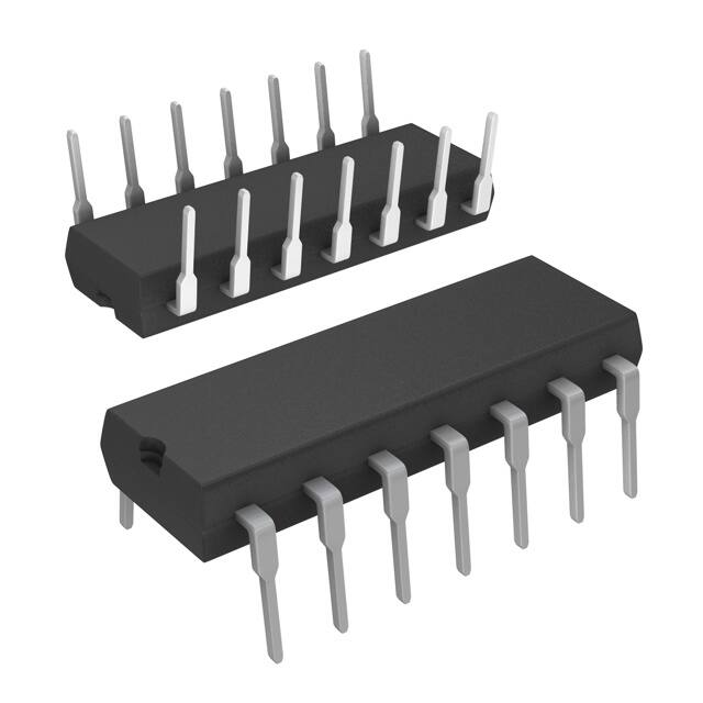


 工商网监
湘ICP备2023018690号
工商网监
湘ICP备2023018690号
