TLD2132-1EP
LITIX™ Basic+
Features
•
Single channel device with integrated and protected output stage (current
source), optimized to drive LEDs as additional low cost current source
•
High output current (up to 240 mA)
•
Very low current consumption in sleep mode
•
Very low output leakage when channel is “off”
•
Low current consumption during fault
•
Output currents’ control via external low power resistor
•
Additional output current demand supported by LITIX™ Companion direct drive without additional
components
•
Very high precision digital dimming supported
•
Intelligent fault management: up to 16 and more devices can share a common error network with only one
external resistor
•
Reverse polarity protection allows reduction of external components and improves system performance
at low battery/input voltages
•
Overload protection
•
Wide temperature range: -40°C < TJ < 150°C
•
Output current control via external low power resistor
•
Green product (RoHS compliant)
Potential applications
•
Cost effective “stop”/ “tail” function implementation with shared and separated LEDs per function
•
Turn indicators
•
Position, fog, rear lights and side markers
•
Animated light functions like wiping indicators and “welcome/goodbye” functions
•
Day Running Light
•
Interior lighting functions like ambient lighting (including RGB color control), illumination and dash board
lighting
•
LED indicators for industrial applications and instrumentation
Product validation
Qualified for Automotive Applications. Product Validation according to AEC-Q100/101.
Datasheet
www.infineon.com
1
Rev. 1.20
2021-06-15
�TLD2132-1EP
LITIX™ Basic+
Description
The LITIX™ Basic+ TLD2132-1EP is a single channel high-side driver IC with integrated output stage. It is
designed to control LEDs with a current up to 240 mA. In typical automotive applications the device is capable
of driving 3 red LEDs with a current up to 180 mA and even above, if not limited by the overall system thermal
properties. Practically, the output current is controlled by an external resistor or reference source,
independently from load and supply voltage changes.
Table 1
Product summary
Parameter
Symbol
Values
Operating voltage
VS(nom)
5.5 V … 40 V
Maximum voltage
VS(max)
VOUT(max)
40 V
Nominal output (load) current
IOUT(nom)
180 mA (nominal) when using the automotive
supply voltage range 8 V - 18 V. Currents up to
IOUT(max) are possible with low thermal resistance
RthJA
Maximum output (load) current
IOUT(max)
240 mA depending on RthJA
Current accuracy at RSET = 10 kΩ
KLT
900 ±5%
Current consumption in sleep mode
IS(sleep, typ)
0.1 µA
Maximum current consumption during IS(fault, ERRN)
fault
850 µA or less when fault is detected from another
device (disabled via ERRN)
Type
Package
Marking
TLD2132-1EP
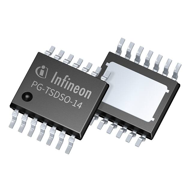
PG-TSDSO-14
TLD2132
Datasheet
2
Rev. 1.20
2021-06-15
�TLD2132-1EP
LITIX™ Basic+
Table of Contents
1
Block diagram . . . . . . . . . . . . . . . . . . . . . . . . . . . . . . . . . . . . . . . . . . . . . . . . . . . . . . . . . . . . . . . . . . . 4
2
2.1
2.2
Pin configuration . . . . . . . . . . . . . . . . . . . . . . . . . . . . . . . . . . . . . . . . . . . . . . . . . . . . . . . . . . . . . . . . . 5
Pin assignment . . . . . . . . . . . . . . . . . . . . . . . . . . . . . . . . . . . . . . . . . . . . . . . . . . . . . . . . . . . . . . . . . . . . . . . . . . . 5
Pin definitions and functions . . . . . . . . . . . . . . . . . . . . . . . . . . . . . . . . . . . . . . . . . . . . . . . . . . . . . . . . . . . . . . 5
3
3.1
3.2
3.3
General product characteristics . . . . . . . . . . . . . . . . . . . . . . . . . . . . . . . . . . . . . . . . . . . . . . . . . . . .
Absolute maximum ratings . . . . . . . . . . . . . . . . . . . . . . . . . . . . . . . . . . . . . . . . . . . . . . . . . . . . . . . . . . . . . . . .
Functional range . . . . . . . . . . . . . . . . . . . . . . . . . . . . . . . . . . . . . . . . . . . . . . . . . . . . . . . . . . . . . . . . . . . . . . . . .
Thermal resistance . . . . . . . . . . . . . . . . . . . . . . . . . . . . . . . . . . . . . . . . . . . . . . . . . . . . . . . . . . . . . . . . . . . . . . .
4
4.1
4.2
Internal supply . . . . . . . . . . . . . . . . . . . . . . . . . . . . . . . . . . . . . . . . . . . . . . . . . . . . . . . . . . . . . . . . . . 10
Description . . . . . . . . . . . . . . . . . . . . . . . . . . . . . . . . . . . . . . . . . . . . . . . . . . . . . . . . . . . . . . . . . . . . . . . . . . . . . 10
Electrical characteristics internal supply and EN pin . . . . . . . . . . . . . . . . . . . . . . . . . . . . . . . . . . . . . . . . 12
5
5.1
5.1.1
5.1.2
5.2
5.2.1
5.2.2
5.2.3
5.2.4
5.2.5
5.2.6
5.2.7
5.3
5.4
Power stage . . . . . . . . . . . . . . . . . . . . . . . . . . . . . . . . . . . . . . . . . . . . . . . . . . . . . . . . . . . . . . . . . . . .
Protection . . . . . . . . . . . . . . . . . . . . . . . . . . . . . . . . . . . . . . . . . . . . . . . . . . . . . . . . . . . . . . . . . . . . . . . . . . . . . .
Thermal protection . . . . . . . . . . . . . . . . . . . . . . . . . . . . . . . . . . . . . . . . . . . . . . . . . . . . . . . . . . . . . . . . . . . .
Reverse battery protection . . . . . . . . . . . . . . . . . . . . . . . . . . . . . . . . . . . . . . . . . . . . . . . . . . . . . . . . . . . . . .
Output configuration via IN_SET, OUT_SET and PWMI pins . . . . . . . . . . . . . . . . . . . . . . . . . . . . . . . . . .
IN_SET pin . . . . . . . . . . . . . . . . . . . . . . . . . . . . . . . . . . . . . . . . . . . . . . . . . . . . . . . . . . . . . . . . . . . . . . . . . . . .
Output current adjustment via RSET . . . . . . . . . . . . . . . . . . . . . . . . . . . . . . . . . . . . . . . . . . . . . . . . . . . . . .
Output control via IN_SET . . . . . . . . . . . . . . . . . . . . . . . . . . . . . . . . . . . . . . . . . . . . . . . . . . . . . . . . . . . . . .
IN_SET pin behavior during device fault management . . . . . . . . . . . . . . . . . . . . . . . . . . . . . . . . . . . . .
OUT_SET pin . . . . . . . . . . . . . . . . . . . . . . . . . . . . . . . . . . . . . . . . . . . . . . . . . . . . . . . . . . . . . . . . . . . . . . . . . .
Direct control of PWMI . . . . . . . . . . . . . . . . . . . . . . . . . . . . . . . . . . . . . . . . . . . . . . . . . . . . . . . . . . . . . . . . .
Timing diagrams . . . . . . . . . . . . . . . . . . . . . . . . . . . . . . . . . . . . . . . . . . . . . . . . . . . . . . . . . . . . . . . . . . . . . . .
Electrical characteristics power stage . . . . . . . . . . . . . . . . . . . . . . . . . . . . . . . . . . . . . . . . . . . . . . . . . . . . . .
Electrical characteristics IN_SET, OUT_SET and PWMI pins for output settings . . . . . . . . . . . . . . . . .
14
14
14
15
15
15
15
16
17
17
18
18
20
22
6
6.1
6.1.1
6.1.2
6.2
6.2.1
6.2.2
6.3
6.3.1
6.3.2
6.3.3
6.3.4
24
24
24
26
27
27
29
31
32
33
33
6.3.5
6.4
Load diagnosis . . . . . . . . . . . . . . . . . . . . . . . . . . . . . . . . . . . . . . . . . . . . . . . . . . . . . . . . . . . . . . . . . .
Error management via ERRN and D-pins . . . . . . . . . . . . . . . . . . . . . . . . . . . . . . . . . . . . . . . . . . . . . . . . . . .
ERRN pin . . . . . . . . . . . . . . . . . . . . . . . . . . . . . . . . . . . . . . . . . . . . . . . . . . . . . . . . . . . . . . . . . . . . . . . . . . . . . .
D-pin . . . . . . . . . . . . . . . . . . . . . . . . . . . . . . . . . . . . . . . . . . . . . . . . . . . . . . . . . . . . . . . . . . . . . . . . . . . . . . . . .
Open Load (OL) and short OUT to GND (SC) . . . . . . . . . . . . . . . . . . . . . . . . . . . . . . . . . . . . . . . . . . . . . . . .
Fault management (D-pin open or connected with a capacitor to GND) . . . . . . . . . . . . . . . . . . . . .
Fault management (D-pin connected to GND) . . . . . . . . . . . . . . . . . . . . . . . . . . . . . . . . . . . . . . . . . . . .
Single LED Short detection, SLS_REF and DS pins . . . . . . . . . . . . . . . . . . . . . . . . . . . . . . . . . . . . . . . . . . .
SLS_REF pin . . . . . . . . . . . . . . . . . . . . . . . . . . . . . . . . . . . . . . . . . . . . . . . . . . . . . . . . . . . . . . . . . . . . . . . . . . .
DS pin . . . . . . . . . . . . . . . . . . . . . . . . . . . . . . . . . . . . . . . . . . . . . . . . . . . . . . . . . . . . . . . . . . . . . . . . . . . . . . . .
SLS fault detection . . . . . . . . . . . . . . . . . . . . . . . . . . . . . . . . . . . . . . . . . . . . . . . . . . . . . . . . . . . . . . . . . . . . .
SLS fault management: D and DS pins open or connected with capacitors to GND (low power
consumption mode with retry strategy) 33
SLS fault management: D-pin shorted to GND . . . . . . . . . . . . . . . . . . . . . . . . . . . . . . . . . . . . . . . . . . . .
Electrical characteristics: Load diagnosis and Overload management . . . . . . . . . . . . . . . . . . . . . . . . .
7
Application information . . . . . . . . . . . . . . . . . . . . . . . . . . . . . . . . . . . . . . . . . . . . . . . . . . . . . . . . . . 38
8
Package outline . . . . . . . . . . . . . . . . . . . . . . . . . . . . . . . . . . . . . . . . . . . . . . . . . . . . . . . . . . . . . . . . . 39
9
Revision History . . . . . . . . . . . . . . . . . . . . . . . . . . . . . . . . . . . . . . . . . . . . . . . . . . . . . . . . . . . . . . . . . 40
Datasheet
3
7
7
8
9
34
35
Rev. 1.20
2021-06-15
�TLD2132-1EP
LITIX™ Basic+
Block diagram
1
Block diagram
10
9
EN/DEN
7
D
5
DS
6
PWMI
4
IN_SET
Datasheet
SLS_REF
Output
control
&
protection
Current
reference
TLD2132-1EP
Figure 1
ERRN
Internal
supply
Thermal
protection
VS
OUT
OUT_SET
14
1
12
2
GND
8
Block diagram
4
Rev. 1.20
2021-06-15
�TLD2132-1EP
LITIX™ Basic+
Pin configuration
2
Pin configuration
2.1
Pin assignment
SLS_REF
OUT_SET
n.c
IN_SET
DS
PWMI
D
1
14
2
13
3
12
EP
4
11
5
10
6
9
exposed pad (bottom)
7
8
TLD2132-1EP
ERRN
n.c
OUT
n.c.
VS
EN/DEN
GND
Figure 2
Pin configuration
2.2
Pin definitions and functions
Pin
Symbol
Function
10
VS
Supply voltage; Connected to battery or supply control switch, with EMC
filter
8
GND
Ground; Signal ground
4
IN_SET
Control input for OUT channel; Connect to a low power resistor to adjust
OUT output current. Alternatively, a different current reference (i.e. the
OUT_SET of another LITIX™ Basic+ LED Driver) may be connected
2
OUT_SET
Control output for additional current source; If an additional channel or
output current with same input control is needed, connect this pin to the
IN_SET pin of the additional LED driver. If not used, leave the pin open
6
PWMI
PWM input; Connect to an external PWM controller. If not used, connect to
GND
1
SLS_REF
Single LED short reference input; Connect to a low power resistor or a
voltage reference to adjust Internal SLS threshold. If not used, connect to
GND
5
DS
Single LED short delay/restart input; Connect to a capacitor, leave open or
connect to GND, depending on the required diagnosis management for single
LED short detection (see Chapter 6 for further details)
7
D
Disable/delay error input; Connect to a capacitor, leave open or connect to
GND, depending on the required diagnosis management (see Chapter 6 for
further details)
14
ERRN
ERROR flag I/O; Open drain, active low. Connect to a pull-up resistor
Datasheet
5
Rev. 1.20
2021-06-15
�TLD2132-1EP
LITIX™ Basic+
Pin configuration
Pin
Symbol
Function
9
EN/DEN
Output enable and diagnosis control input; Connect to a control input (i.e.
to VS via a resistor divider or a Zener diode) to enable OUT control and
diagnosis capability
12
OUT
Channel output; Connect to the target load
3, 11, 13
n.c.
Not connected; Leave these pins open
Exposed
Pad
EP
Exposed Pad; Connected to GND-pin in application
Datasheet
6
Rev. 1.20
2021-06-15
�TLD2132-1EP
LITIX™ Basic+
General product characteristics
3
General product characteristics
3.1
Absolute maximum ratings
Table 2
Absolute maximum ratings1)
TJ = -40°C to +150°C; RIN_SET = 10 kΩ; all voltages with respect to GND, positive current flowing into input and
I/O pins, positive current flowing out from output pins (unless otherwise specified)
Parameter
Symbol
Values
Min.
Typ.
Max.
Unit
Note or
Test Condition
Number
Voltage
Supply voltage
VS
-18
–
40
V
–
P_4.1.1
EN/DEN voltage
VEN/DEN
-18
–
40
V
–
P_4.1.3
EN/DEN voltage related to VS:
VEN/DEN - VS
VEN/DEN(VS -40
–
18
V
–
P_4.1.4
–
40
V
–
P_4.1.5
-1
–
40
V
–
P_4.1.10
Output voltage related to VS: VS - VOUT(VS)
VOUT
-18
–
40
V
–
P_4.1.11
IN_SET voltage
VIN_SET
-0.3
–
6
V
–
P_4.1.12
OUT_SET voltage
VOUT_SET
-0.3
–
6
V
–
P_4.1.13
PWMI voltage
VPWMI
-0.3
–
6
V
–
P_4.1.14
ERRN voltage
VERRN
-0.3
–
40
V
–
P_4.1.18
D Voltage
VD
-0.3
–
6
V
–
P_4.1.19
DS voltage
VDS
-0.3
–
6
V
–
P_4.1.42
SLS_REF voltage
VSLS_REF
-0.3
–
6
V
–
P_4.1.43
Output current
IOUT
0
–
250
mA
–
P_4.1.23
PWMI current
IPWMI
-0.5
–
0.5
mA
–
P_4.1.26
IN_SET current
IIN_SET
0
–
300
µA
–
P_4.1.30
D current
ID
-0.5
–
0.5
mA
–
P_4.1.31
DS current
IDS
-0.5
–
0.5
mA
–
P_4.1.44
SLS_REF current
ISLS_REF
-0.5
–
0
mA
–
P_4.1.45
OUT_SET current
IOUT_SET
0
–
0.5
mA
–
P_4.1.32
Junction temperature
TJ
-40
–
150
°C
–
P_4.1.33
Storage temperature
Tstg
-55
–
150
°C
–
P_4.1.34
VESD
-2
–
2
kV
HBM2)
P_4.1.36
)
EN/DEN voltage related to VOUT: VEN/DEN(V -18
VEN/DEN - VOUT
OUT)
Output voltage
VOUT
Current
Temperature
ESD susceptibility
ESD susceptibility all pins to
GND
Datasheet
7
Rev. 1.20
2021-06-15
�TLD2132-1EP
LITIX™ Basic+
General product characteristics
Table 2
Absolute maximum ratings1) (cont’d)
TJ = -40°C to +150°C; RIN_SET = 10 kΩ; all voltages with respect to GND, positive current flowing into input and
I/O pins, positive current flowing out from output pins (unless otherwise specified)
Parameter
Symbol
Values
Unit
Note or
Test Condition
Number
Min.
Typ.
Max.
-500
–
500
V
CDM3)
P_4.1.37
ESD susceptibility Pin 1, 7, 8, 14 VESD1,7,8,1 -750
(corner pins) to GND
4
–
750
V
CDM3)
P_4.1.38
ESD susceptibility all pins to
GND
VESD
1) Not subject to production test, specified by design
2) ESD susceptibility, HBM according to ANSI/ESDA/JEDEC JS001 (1.5 kΩ, 100 pF)
3) ESD susceptibility, Charged Device Model “CDM” according JEDEC JESD22-C101
Notes
1. Stresses above the ones listed here may cause permanent damage to the device. Exposure to absolute
maximum rating conditions for extended periods may affect device reliability.
2. Integrated protection functions are designed to prevent IC destruction under fault conditions described in the
data sheet. Fault conditions are considered as “outside” normal operating range. Protection functions are
not designed for continuous repetitive operation.
3.2
Functional range
Table 3
Functional range
Parameter
Symbol
Values
Unit
Note or
Test Condition
Number
Min.
Typ.
Max.
5.5
–
18
V
–
P_4.2.1
Extended supply voltage for VS(ext)
functional range
VSUV(ON) –
40
V
–
P_4.2.2
Junction temperature
-40
150
°C
–
P_4.2.4
Voltage range for normal
operation
Note:
Datasheet
VS(nom)
TJ
–
Within the Normal Operation range, the IC operates as described in the circuit description. Within the
Extended Operation range, parameters deviations are possible. The electrical characteristics are
specified within the conditions given in the Electrical Characteristics table.
8
Rev. 1.20
2021-06-15
�TLD2132-1EP
LITIX™ Basic+
General product characteristics
3.3
Thermal resistance
Note:
This thermal data was generated in accordance with JEDEC JESD51 standards. For more
information, go to www.jedec.org.
Table 4
Thermal resistance1)
Parameter
Junction to Case
Symbol
RthJC
Junction to Ambient 1s0p
board
RthJA1
Junction to Ambient 2s2p
board
RthJA2
Values
Min.
Typ.
Max.
–
–
10
–
–
61
56
Unit
Note or
Test Condition
Number
K/W
1)2)
P_4.3.1
K/W
1)3)
P_4.3.3
–
–
TA = 85°C
TA = 135°C
K/W
–
–
45
43
–
–
1)4)
P_4.3.4
TA = 85°C
TA = 135°C
1) Not subject to production test, specified by design
2) Specified RthJC value is simulated at natural convection on a cold plate setup (all pins and exposed pad are fixed to
ambient temperature). TA = 85°C. Total power dissipation = 1.5 W
3) Specified RthJA value is according to Jedec JESD51-3 at natural convection on FR4 1s0p board. The product
(chip+package) was simulated on a 76.2 × 114.3 × 1.5 mm board with 70 µm Cu, 300 mm2 cooling area. Total power
dissipation 1.5 W distributed statically and homogenously over all power stages
4) Specified RthJA value is according to Jedec JESD51-5,-7 at natural convection on FR4 2s2p board; The product
(chip+package) was simulated on a 76.2 × 114.3 × 1.5 mm board with 2 inner copper layers (2 × 70 µm Cu, 2 × 35 µm
Cu). Where applicable a thermal via array under the exposed pad contacted the first inner copper layer. Total power
dissipation 1.5 W distributed statically and homogenously over all power stages
Datasheet
9
Rev. 1.20
2021-06-15
�TLD2132-1EP
LITIX™ Basic+
Internal supply
4
Internal supply
This chapter describes the internal supply in its main parameters and functionality.
4.1
Description
The internal supply principle is highlighted in the concept diagram of Figure 3.
If the voltage applied at the EN/DEN pin is below VEN(th) the device enters sleep mode. In this state all internal
functions are switched off and the current consumption is reduced to IS(sleep) .
As soon as the voltage applied at the supply pin VS is above VSUV(ON) and the voltage applied at the EN/DEN pin
is above VEN(th), after the power-on reset time tPOR, the device is ready to deliver output current from the output
stage. The power on reset time tPOR has to be taken into account also in relevant application conditions, i. e.
with PWM control from VS or EN/DEN lines.
VSUV
-
VS
+
Internal
Supply
VEN(th)
OUTx
Control
EN/DEN
+
OUTx
Diagnosis
Control
+
VDEN(th)
Figure 3
Internal supply
Furthermore, as soon as the voltage applied at the supply pin VS is above VSUV(ON) and the voltage applied to
the EN/DEN pin VEN is above VDEN(th), the device is ready to detect and report fault conditions via ERRN (error
network pin) as described in Chapter 6.
To program output enable and diagnosis enable via EN/DEN pin there are several possibilities, like a resistor
divider from VS to GND, a Zener diode from EN/DEN to VS and also a logic control pin (e.g. from a
microcontroller output).
Datasheet
10
Rev. 1.20
2021-06-15
�TLD2132-1EP
LITIX™ Basic+
Internal supply
VS
V SU V(th)
t
VEN
V EN (th)
IOUT
t
tPO R
100%
80%
t
Figure 4
Datasheet
Power on reset timing diagram
11
Rev. 1.20
2021-06-15
�TLD2132-1EP
LITIX™ Basic+
Internal supply
4.2
Table 5
Electrical characteristics internal supply and EN pin
Electrical characteristics: Internal supply and EN pin
TJ = -40°C to +150°C; VS =5.5 V to 18 V; RIN_SET = 10 kΩ; all voltages with respect to GND, positive current flowing
into input and I/O pins, positive current flowing out from output pins (unless otherwise specified)
Parameter
Symbol
Values
Unit
Note or
Test Condition
Number
Min.
Typ.
Max.
Current consumption, sleep IS(sleep)
mode
–
0.1
2
µA
1)
VEN = 0 V
TJ < 85°C
VS = 18 V
VOUT = 3.6 V
P_5.2.1
Current consumption, active IS(active)
mode (no fault)
–
1.5
3
mA
VEN = 5.5 V
IIN_SET = 0 µA
TJ < 105°C
VS = 18 V
VOUT = 3.6 V
P_5.2.3
Current consumption during IS(fault, ERRN)
fault condition triggered
from another device sharing
ERRN bus
–
–
850
µA
VEN = 5.5 V
TJ < 105°C
VS = 18 V
VERRN = 0 V
VOUT = 3.6 V
D open
P_5.2.4
Current consumption during IS(fault, OUT)
fault condition
–
–
1.25
mA
VEN = 5.5 V
TJ < 105°C
VS = 18 V
VOUT = 0 V
VOUT
D open
P_5.2.16
Required supply voltage for VSUV(ON)
output activation
–
–
5.5
V
VEN = VS
P_5.2.5
VOUT = 3 V
RIN_SET = 6.8 kΩ
IOUT > 50% IOUT(nom)
Required supply voltage for VSUV(OFF)
output deactivation
4.5
–
–
V
VEN = VS
P_5.2.6
VOUT = 3 V
RIN_SET = 6.8 kΩ
IOUT < 50% IOUT(nom)
VSUV(hys)
Supply voltage activation
hysteresis: VSUV(ON) - VSUV(OFF)
–
200
–
mV
1)
EN output enable threshold VEN(th)
1.4
1.65
1.8
V
VS = 5.5 V
P_5.2.9
VPS = 2 V
RIN_SET = 6.8 kΩ
IOUT = 50% IOUT(nom)
DEN diagnosis enable
threshold
2.4
2.5
2.8
V
VS = 5.5 V
Supply thresholds
VEN > VEN(th)
P_5.2.8
EN pin
Datasheet
VDEN(th)
12
P_5.2.11
Rev. 1.20
2021-06-15
�TLD2132-1EP
LITIX™ Basic+
Internal supply
Table 5
Electrical characteristics: Internal supply and EN pin (cont’d)
TJ = -40°C to +150°C; VS =5.5 V to 18 V; RIN_SET = 10 kΩ; all voltages with respect to GND, positive current flowing
into input and I/O pins, positive current flowing out from output pins (unless otherwise specified)
Parameter
Symbol
Values
Min.
Typ.
Max.
Unit
Note or
Test Condition
Number
P_5.2.12
DEN diagnosis enable
hysteresis
VDEN(hys)
–
120
–
mV
1)
EN/DEN pull-down current
IEN/DEN(PD)
–
–
15
µA
1)
VS > 8 V
VEN/DEN = 2.8 V
P_5.2.17
EN/DEN pull-down current
IEN/DEN(PD)
–
–
35
µA
1)
VS > 8 V
VEN/DEN = 5.5 V
P_5.2.14
EN/DEN pull-down current
IEN/DEN(PD)
–
–
150
µA
1)
VS > 8 V
VEN/DEN = VS
P_5.2.15
tPOR
–
–
25
µs
1)
RIN_SET = 6.8 kΩ
Timing
Power on reset delay time
VS rising from 0 V P_5.2.13
to 13.5 V
VOUT = 3.6 V
RIN_SET = 6.8 kΩ
IOUT = 80% IOUT(nom)
1) Not subjected to production test: specified by design
Datasheet
13
Rev. 1.20
2021-06-15
�TLD2132-1EP
LITIX™ Basic+
Power stage
5
Power stage
The output stage is realized as high-side current source with an output current up to 240mA. During off state
the leakage current at the output stage is minimized in order to prevent a slightly glowing LED.
The maximum output current is limited by the power dissipation and used PCB cooling areas.
For an operating output current control loop, the supply and output voltage have to be considered according
to the following parameters:
•
Required supply voltage for current control VS(CC)
•
Voltage drop over through the output stage during current control VPS(CC)
•
Required output voltage for current control VOUT(CC)
5.1
Protection
The device provides embedded protective functions, which are designed to prevent IC damage under fault
conditions described in this datasheet. Fault conditions are considered as “outside” normal operating range.
Protective functions are not designed for continuous nor for repetitive operations.
5.1.1
Thermal protection
A thermal protection circuitry is integrated in the device. It is realized by a temperature monitoring of the
output stages.
As soon as the junction temperature exceeds the current reduction temperature threshold TJ(CRT) the output
current can be reduced by the device by reducing the IN_SET reference voltage VIN_SET(ref). This feature greatly
helps to avoid LEDs flickering during static output overload conditions. Furthermore, it helps to protect the
LEDs, which are mounted thermally close to the device, against overtemperature. If the device temperature
still increases, the three output currents decrease close to 0 A. As soon as the device cools down the output
currents rise again.
IOUT
VIN _SE T
Tj(CRT)
Figure 5
Note:
Datasheet
Tj
Output current reduction at high temperature (qualitative diagram)
It is assumed that a configuration resistor RSET is applied from IN_SET to GND, and not a current
source, to make the protection effective.
14
Rev. 1.20
2021-06-15
�TLD2132-1EP
LITIX™ Basic+
Power stage
5.1.2
Reverse battery protection
The device has an integrated reverse battery protection feature. This feature protects the driver IC itself and,
potentially, also connected LEDs. The output reverse current is limited to IOUT(REV) by the reverse battery
protection.
5.2
Output configuration via IN_SET, OUT_SET and PWMI pins
Outputs current can be defined via IN_SET and OUT_SET (to drive additional devices without further external
components) pin.
5.2.1
IN_SET pin
The IN_SET pin is a multiple function pin for the output current definition and input control.
Output current definition and analog dimming control can be done defining accordingly the IN_SET current.
ref/fault selection
logic
IN_SET
IIN_SET
VIN_SET(ref)
IIN_SET(faul t)
GND
Figure 6
5.2.2
IN_SET pin block diagram
Output current adjustment via RSET
The output current for the channel can be defined connecting a low power resistor (RSET) between the IN_SET
pin and GND. The dimensioning of the resistor can be done using the formula:
(5.1)
I OUT = k ⋅ I IN _ SET = k ⋅ VIN _ SET ( ref ) / RSET
The gain factor k (defined as the ratio IOUT/IIN_SET) is graphically described in Figure 7.
The current through the RSET is defined by the resistor itself and the reference voltage VIN_SET(ref), which is
applied to the IN_SET pin when the device is supplied and the channel enabled.
Datasheet
15
Rev. 1.20
2021-06-15
�TLD2132-1EP
LITIX™ Basic+
Power stage
5.2.3
Output control via IN_SET
The IN_SET pin can be connected via RSET to the open-drain output of a microcontroller or to an external
NMOS transistor as described in Figure 9. This signal can be used to turn off the relative output stages of the
IC.
A minimum IN_SET current of IIN_SET(ACT) is required to turn on the output stages. This feature is implemented
to prevent glowing of LEDs caused by leakage currents on the IN_SET pin, see again Figure 7 for details.
IOUT [mA]
k = IOUT / IIN_SET
IOUT
IIN_SET(ACT)
Figure 7
IIN_SET
IIN_SET [µA]
IOUT vs IIN_SET
k/k(typ)
105%
100%
95%
33
Figure 8
Datasheet
66
100
150
200
IIN_SET
[µA]
267
Typical output current accuracy IOUT / IIN_SET at TJ = 25°C
16
Rev. 1.20
2021-06-15
�TLD2132-1EP
LITIX™ Basic+
Power stage
VS
Supply
Protection
Microcontroller
OUT
RSET
EN
VS
LITIX™
Basic+ (*)
IN_SET
OUT
PWMI
GND
(*) The drawing refers to a generic LITIX™ BASIC+ device,
and does not represent a specific device pinout
(only the relevant connections for microcontroller IN_SET control are shown)
Figure 9
5.2.4
Output control via IN_SET pin and open-drain microcontroller out (simplified diagram)
IN_SET pin behavior during device fault management
If a fault condition arises on the channel controlled by the IN_SET pin, once the D-pin reaches the high level
threshold VD(th), the current of the IN_SET pin is reduced to IIN_SET(fault), in order to minimise the current
consumption of the whole device under fault condition (detailed description is in the load diagnosis section,
Chapter 6).
5.2.5
OUT_SET pin
The OUT_SET pin, mirroring the IN_SET current defined by the external resistor RSET, can be used to define the
IN_SET current of an additional companion device.
If minimum IN_SET activation current IIN_SET(act) is not reached or if the D-pin reaches the high level threshold
VD(th) the OUT_SET current is reduced to IOUT_SET(OFF). This allows to drive other devices via OUT_SET, even when
digital dimming is required, without external components (see application drawing example in Chapter 7).
Datasheet
17
Rev. 1.20
2021-06-15
�TLD2132-1EP
LITIX™ Basic+
Power stage
LOGIC
OUT_SET
IOUT_SET
IOUT_SET(OFF)
IOUT_SET(ON)
GND
Figure 10
OUT_SET pin block diagram
LITIX™
Basic+ (*)
RSET
IN_SET
OUT_SET
OUT
PWMI
GND
LITIX™
Basic+ (*)
IN_SET
OUT_SET
OUT
PWMI
GND
EN
VS
EN
VS
EN
Supply
Protection
VS
VS
LITIX™
Basic+ (*)
IN_SET
OUT_SET
OUT
PWMI
GND
(*) The drawing refers to a generic LITIX™ BASIC+ device,
and does not represent a specific device pinout
(only the relevant connections are shown)
Figure 11
5.2.6
IN_SET to OUT_SET serial connection example
Direct control of PWMI
PWMI input can be controlled by the PWMO output of another device of LITIX™ Basic+ family or, alternatively,
a push-pull output stage of a microcontroller: the host device decides the digital dimming characteristics by
applying the proper control cycle in order to set the “on”/“off” timing, according to the chosen dimming
function.
5.2.7
Timing diagrams
In the following diagrams (Figure 12, Figure 13, Figure 14) the influences of different driving inputs on output
activation delays are shown.
Datasheet
18
Rev. 1.20
2021-06-15
�TLD2132-1EP
LITIX™ Basic+
Power stage
I IN_SET
IOUT
tON(IN_SET )
t
tOFF(IN_SET )
100%
90%
10%
t
Figure 12
IN_SET turn on and turn off delay timing diagram
IIN _SET
I OUT_SET
tdel ( OUT _SET ,H)
tdel( OUT _SET ,L)
t
100%
90%
10%
t
Figure 13
IN_SET to OUT_SET activation and deactivation delay timing diagram
V PWMI
IOUT
tOFF (PWMI )
tON(PWMI )
t
100%
90%
10%
t
Figure 14
Datasheet
PWMI turn on and turn off timing diagram
19
Rev. 1.20
2021-06-15
�TLD2132-1EP
LITIX™ Basic+
Power stage
5.3
Table 6
Electrical characteristics power stage
Electrical characteristics: Power stage
TJ = -40°C to +150°C; VS =5.5 V to 18 V; RIN_SET = 10 kΩ; all voltages with respect to GND, positive current flowing
into input and I/O pins, positive current flowing out from output pins (unless otherwise specified)
Parameter
Symbol
Values
Min.
Typ.
Max.
Unit
Note or
Test Condition
Number
Output leakage current
IOUT(leak)
–
–
9
µA
1)
VEN = 5.5 V
IIN_SET = 0 µA
VOUT = 2.5 V
TJ = 85°C
P_6.5.51
Output leakage current
IOUT(leak)
–
–
21
µA
1)
VEN = 5.5 V
IIN_SET = 0 µA
VOUT = 2.5 V
TJ = 150°C
P_6.5.60
Reverse output current
IOUT(rev)
–
–
3
µA
1)
VEN = Vs
VS = -18 V
Output load: LED
with break down
voltage < - 0.6 V
P_6.5.2
Output current accuracy
KLT
837
900
963
–
1)
TJ = 25... 115°C
VS = 8... 18 V
VPS = 2 V
IIN_SET = 33 µA
P_6.5.53
Output current accuracy
KALL
801
900
999
–
1)
TJ = -40... 115°C
VS = 8... 18 V
VPS = 2 V
IIN_SET = 33 µA
P_6.5.54
Output current accuracy
KLT
855
900
945
–
1)
TJ = 25... 115°C
VS = 8... 18 V
VPS = 2 V
IIN_SET = 66 µA
P_6.5.55
Output current accuracy
KALL
837
900
963
–
1)
TJ = -40... 115°C
VS = 8... 18 V
VPS = 2 V
IIN_SET = 66 µA
P_6.5.56
Output current accuracy
KLT
864
900
936
–
1)
TJ = 25... 115°C
VS = 8... 18 V
VPS = 2 V
IIN_SET = 200 µA
P_6.5.57
Output current accuracy
KALL
855
900
945
–
1)
P_6.5.58
Output current accuracy
Datasheet
20
TJ = -40... 115°C
VS = 8... 18 V
VPS = 2 V
IIN_SET = 200 µA
Rev. 1.20
2021-06-15
�TLD2132-1EP
LITIX™ Basic+
Power stage
Table 6
Electrical characteristics: Power stage (cont’d)
TJ = -40°C to +150°C; VS =5.5 V to 18 V; RIN_SET = 10 kΩ; all voltages with respect to GND, positive current flowing
into input and I/O pins, positive current flowing out from output pins (unless otherwise specified)
Parameter
Symbol
Values
Min.
Typ.
Max.
Unit
Note or
Test Condition
Number
Required voltage drop
during current control
VPS(CC) = VS - VOUT
VPS(CC)
1.0
–
–
V
2)
VS = 8... 18 V
IOUT > 90% of
K(typ)*IIN_SET
P_6.5.36
Required voltage drop
during current control
VPS(CC) = VS - VOUT
VPS(CC)
0.65
–
–
V
2)
VS = 8... 18 V
IIN_SET = 133 µA
IOUT > 90% of
K(typ)*IIN_SET
TJ = -40°C
P_6.5.37
Required voltage drop
during current control
VPS(CC) = VS - VOUT
VPS(CC)
0.75
–
–
V
2)
VS = 8... 18 V
IIN_SET = 133 µA
IOUT > 90% of
K(typ)*IIN_SET
TJ = 25°C
P_6.5.38
Required voltage drop
during current control
VPS(CC) = VS - VOUT
VPS(CC)
0.85
–
–
V
2)
VS = 8... 18V
IIN_SET = 133 µA
IOUT > 90% of
K(typ)*IIN_SET
TJ = 150°C
P_6.5.39
Required supply voltage for VS(CC)
current control
5.5
–
–
V
VEN = 5.5 V
VOUT = 3 V
RIN_SET = 6.8 kΩ
IOUT > 90% of
K*IIN_SET
P_6.5.40
Required output voltage for VOUT(CC)
current control
1.4
–
–
V
VS = 8... 18 V
IOUT > 90% of
K*IIN_SET
P_6.5.41
Current reduction
temperature threshold
TJ(CRT)
–
140
–
°C
1)
P_6.5.44
Output current during
current reduction at high
temperature
IOUT(CRT)
85% of –
IOUT(typ)
–
mA
1)
TJ = 150°C
P_6.5.45
1) Not subjected to production test: specified by design
2) In these test conditions, the parameter K(typ) represents the typical value of output current accuracy.
Datasheet
21
Rev. 1.20
2021-06-15
�TLD2132-1EP
LITIX™ Basic+
Power stage
5.4
Table 7
Electrical characteristics IN_SET, OUT_SET and PWMI pins for output settings
Electrical characteristics: IN_SET, OUT_SET and PWMI pins
TJ = -40°C to +150°C; VS =5.5 V to 18 V; RIN_SET = 10 kΩ; all voltages with respect to GND, positive current flowing
into input and I/O pins, positive current flowing out from output pins (unless otherwise specified)
Parameter
Symbol
Values
Min.
Typ.
Max.
Unit
Note or
Test Condition
Number
IN_SET reference voltage
VIN_SET(ref)
1.195
1.22
1.245
V
1)
VEN = 5.5 V
TJ = 25°C
P_6.6.1
IN_SET reference voltage
VIN_SET(ref)
1.184
1.22
1.256
V
1)
VEN = 5.5 V
TJ = -40... 115°C
P_6.6.17
IN_SET output activation
current
IIN_SET(ACT)
–
–
15
µA
VEN = 5.5 V
VPS = 3 V
IOUT > 50% of
K(typ)*IIN_SET
P_6.6.2
OUT_SET output current
matching
∆IOUT_SET(ON)/II -4
–
4
%
P_6.6.3
N_SET
VS = 8 V to 18 V
VOUT_SET = 1.2V
IIN_SET = 267 µA
PWMI low threshold
VPWMI(L)
1.5
1.7
2
V
VS = 8 V to 18 V
VEN = 5.5 V
P_6.6.6
PWMI high threshold
VPWMI(H)
2.5
2.7
3
V
VS = 8 V to 18 V
VEN = 5.5 V
P_6.6.7
IN_SET turn on time
tON(IN_SET)
–
–
20
µs
1)2)
VS = 13.5 V
P_6.6.8
VPS = 4 V
IIN_SET rising from 0
to 180 µA
IOUT = 90% of
K*IIN_SET
IN_SET turn off time
tOFF(IN_SET)
–
–
10
µs
1)2)
VS = 13.5 V
VPS = 4 V
IIN_SET falling from
180 to 0 µA
IOUT = 10% of
K*IIN_SET
OUT_SET activation time
tdel(OUT_SET,H)
–
–
5
µs
1)3)
VS = 13.5 V
P_6.6.10
IIN_SET rising from 0
to 180 µA
IOUT_SET = 90% of
IIN_SET
OUT_SET deactivation time tdel(OUT_SET,L)
–
–
5
µs
1)3)
Timing
Datasheet
22
VS = 13.5 V
IIN_SET falling from
180 to 0 µA
IOUT_SET = 10% of
IIN_SET
P_6.6.9
P_6.6.11
Rev. 1.20
2021-06-15
�TLD2132-1EP
LITIX™ Basic+
Power stage
Table 7
Electrical characteristics: IN_SET, OUT_SET and PWMI pins (cont’d)
TJ = -40°C to +150°C; VS =5.5 V to 18 V; RIN_SET = 10 kΩ; all voltages with respect to GND, positive current flowing
into input and I/O pins, positive current flowing out from output pins (unless otherwise specified)
Parameter
Symbol
Values
Min.
Typ.
Max.
Unit
Note or
Test Condition
Number
PWMI turn on time
tON(PWMI)
–
–
15
µs
1)4)
VS = 8 V to 18 V
VEN = 5.5 V
VPWMI falling from
5 V to 0 V
IOUT = 90% of
K*IIN_SET
TJ = -40... 115°C
P_6.6.12
PWMI turn off time
tOFF(PWMI)
–
–
10
µs
1)4)
P_6.6.13
1)
2)
3)
4)
VS = 8 V to 18 V
VEN = 5.5 V
VPWMI = 0 rising
from 0 V to 5 V
IOUT = 10% of
K*IIN_SET
TJ = -40... 115°C
Not subjected to production test: specified by design
Refer to Figure 12
Refer to Figure 13
Refer to Figure 14
Datasheet
23
Rev. 1.20
2021-06-15
�TLD2132-1EP
LITIX™ Basic+
Load diagnosis
6
Load diagnosis
6.1
Error management via ERRN and D-pins
Several diagnosis features are integrated in the TLD2132-1EP:
•
Open load detection (OL).
•
Short circuit OUT-GND (SC).
•
Single LED Short detection (SLS).
6.1.1
ERRN pin
ERRN
+
fault
Output
control
no fault
VERR N(th)
IERR N(faul t)
Figure 15
ERRN pin (block diagram)
The device is able to report a detected failure in its driven load and react to a fault detected by another LED
driver in the system if a shared error network is implemented (i. e. driving LED chains of the same light
function). This is possible with the usage of an external pull-up resistor, allowing multiple devices to share the
open drain diagnosis output pin ERRN. All devices sharing the common error network are capable to detect
the fault from any of the channels driven by the LITIX™ Basic+ LED drivers and, if desired, to switch multiple
loads off.
Datasheet
24
Rev. 1.20
2021-06-15
�TLD2132-1EP
LITIX™ Basic+
Load diagnosis
ERRN
OUT
LITIX™
Basic+ (*)
IN_SET
RSET
RSET
IN_SET
PWMI
GND
ERRN
Connection to further devices
LITIX™
Basic+ (*)
EN
VS
EN
VS
Supply
Protection
RERRN
VS
PWMI
GND
OUT
(*) The drawing refers to a generic LITIX™ BASIC+ device,
and does not represent a specific device pinout
(only the relevant connections are shown)
Figure 16
Shared error network principle between LITIX™ Basic+ family devices
When the channel is detected to be under fault conditions (for, at least, a filter time tfault), the open-drain ERRN
pin sinks a pull-down current IERRN(fault) toward GND. Therefore an active low state can be detected at ERRN pin
when VERRN < VERRN(fault) and if this condition is reached, provided the proper setup of the delay pin D, the
channel is switched off. Similarly, when the fault is removed, ERRN pin is put back in high impedance state,
and the channels reactivation procedure can be completed once D-pin voltage is below the value VD(th), as
illustrated in the timing diagrams in this chapter.
Datasheet
25
Rev. 1.20
2021-06-15
�TLD2132-1EP
LITIX™ Basic+
Load diagnosis
6.1.2
D-pin
ID(faul t)
ERRN = H
ERRN = L
CD
D
+
ERRN = H
ERRN = L
-
Output
control
VD(th)
ID(PD)
Figure 17
D-pin (block diagram).
The D-pin is designed for 2 main purposes:
•
To react to error conditions in LED arrays according to the implemented fault management policy, in
systems where multiple LED chains are used for a given light function.
•
To extend the channel deactivation delay time of a value tD, adding a small signal capacitor from the D-pin
to GND. In this way, an unstable or noisy fault condition may be prevented from switching off all the
channels of a given light function (i.e. driven by several driver ICs sharing the same error network).
The functionality of the D-pin is shown in the Figure 17 simplified block diagram:
If one LED within one chain fails in open load condition or the device output is shorted to GND, the respective
LED chain is off. Different automotive applications require a complete deactivation of a light function, if the
desired brightness of the function (LED array) can not be achieved due to an internal error condition.
In normal operative status (no fault) a pull-down current ID(PD) is sunk from the D-pin to GND. If there is a fault
condition (for, at least, a filter time tfault) in one of the LED channels driven by the IC or in any of the devices
sharing the same ERRN error network line, a pull-up current ID(fault) is instead sourced from the D-pin. As a
consequence, if a capacitive or open load is applied at this pin, its voltage starts rising.
When VD(th) is reached at D-pin, all the channels driven by the device are switched off and if other devices share
the same ERRN and D-pins nodes, all the devices turn their outputs off.
Alternatively, if the D-pin is tied to GND, only the channel that has been detected with a fault is safely
deactivated.
The capacitor value used at the D-pin, CD, sets the delay times tD(set/reset) according to the following equations:
𝑡𝐷(𝑠𝑒𝑡 ) =
𝐶𝐷 ∙ 𝑉𝐷(𝑡ℎ)
𝐼𝐷(𝑓𝑎𝑢𝑙𝑡 )
𝑡𝐷(𝑟𝑒𝑠𝑒𝑡 ) =
Datasheet
(6.1)
𝐶𝐷 ∙ 𝑉𝐷(𝐶𝐿) − 𝑉𝐷(𝑡ℎ)
𝐼𝐷(𝑃𝐷)
(6.2)
26
Rev. 1.20
2021-06-15
�TLD2132-1EP
LITIX™ Basic+
Load diagnosis
Note:
If the device detects a Single LED Short failure, the D-pin behavior and the overall fault management
is slightly different (allows periodical retries with load reactivation, according to DS pin settings
too), as described in Chapter 6.3.
6.2
Open Load (OL) and short OUT to GND (SC)
The behavior of the device during overload conditions that lead to an excess of internal heating up to
overtemperature condition, is already described in Chapter 5.
Open load (OL) and OUT shorted to GND (SC) diagnosis features are also integrated in the TLD2132-1EP.
An open load condition is detected if the voltage drop over the output stage VPS is below the threshold VPS(OL)
at least for a filter time tfault.
A short to GND condition is detected if the voltage of the output stages VOUT is below the threshold VOUT(SC) at
least for a filter time tfault.
6.2.1
Fault management (D-pin open or connected with a capacitor to GND)
With D-pin open or connected with a capacitor to GND configuration, it is possible to switch off all the channels
which share a common error network, without the need of an auxiliary microcontroller. For more details refer
also to the timing diagram of Figure 18, Figure 19.
If there is an OL or SC condition on the output, a pull-up current IOUT(fault) then flows out from the channel,
replacing the configured output current (but limited by the actual load impedance, e.g. reduced to zero with
an ideal open load). Under these conditions, the ERRN pin starts sinking a current IERRN(fault) toward GND and
(with proper dimensioning of the external pull-up resistor) reaches a voltage level below VERRN(fault).
After tD(set), the voltage VD(th) is reached at D-pin, the IN_SET goes in a weak pull-down state with a current
consumption IIN_SET(fault) after an additional latency time tIN_SET(del). The ERRN low voltage can also be used as
input signal for a microcontroller to perform the desired diagnosis policy.
The OL and SC error conditions are not latched: as soon as the fault condition is no longer present (at least for
a filter time tfault) ERRN goes back to high impedance. When its voltage is above VERRN(fault), the D-pin voltage
starts decreasing and after tD(reset) goes below (VD(th) - VD(th,hys)). Then the IN_SET voltage goes up to VIN_SET(ref),
again after a time tIN_SET(del): at this point, the output stage are activated again. The total time between the fault
removal and the IN_SET reactivation tERR(reset) is extended by an additional latency which depends on the
external ERRN pin pull-up and filter circuitry.
Datasheet
27
Rev. 1.20
2021-06-15
�TLD2132-1EP
LITIX™ Basic+
Load diagnosis
VIN_SET
VIN _ SET (re f)
V ERRN
tIN _SET (del)
tIN _SET (del)
t
VER R N(fa u l t)
t
VD
VD(th, hy s)
V D( th)
tD(set)
tD(res et)
t
tERR(res et)
VOUT
tfault
tfault
VS
V S – V PS (O L)
VF
open load
occurs
open load
disappears
t
Figure 18
Datasheet
Open load condition timing diagram example (D-pin unconnected or connected to external
capacitor to GND, VF represents the typical forward voltage of the output load)
28
Rev. 1.20
2021-06-15
�TLD2132-1EP
LITIX™ Basic+
Load diagnosis
V IN_SET
V IN _SET (re f)
V ERRN
t IN_SET (del)
t IN_SET (del)
t
VER R N(fa u l t)
t
VD
VD(th, hy s)
VD (th )
tD(s et)
V OUT
t D(res et)
t
t ERR(res et)
t fault
t fault
VS
VF
V O U T(SC )
t
short circuit
occurs
short circuit
disappears
Figure 19
Short circuit to GND condition timing diagram example (D-pin not connected or connected
to external capacitor to GND, VFxyz represents the forward voltage of the output loads)
6.2.2
Fault management (D-pin connected to GND)
With D-pin connected to GND configuration, it is possible to deactivate only the channel under fault
conditions, still sharing ERRN pin in a common error network with other devices of LITIX™ Basic+ family.
If there is fault condition on the output, a pull-up current IOUT(fault) flows out from the channel, replacing the
configured output current (but limited by the actual load impedance, e.g. reduced to zero with an ideal open
load). Under fault conditions the ERRN pin starts sinking a current IERRN(fault) to ground and the voltage level on
this pin will drop below VERRN(fault) if the external pull-up resistor is properly dimensioned. The ERRN low
voltage can also be used as input signal for a µC to perform the desired diagnosis policy.
Datasheet
29
Rev. 1.20
2021-06-15
�TLD2132-1EP
LITIX™ Basic+
Load diagnosis
The fault status is not latched: as soon as the fault condition is no longer present (at least for a filter time tfault),
ERRN goes back to high impedance and, once its voltage is above VERRN(fault), finally the output stages are
activated again.
Examples of open load or short to GND diagnosis with D-pin open or connected to GND are shown in the timing
diagrams of Figure 20 and Figure 21.
VIN _SE T
V IN_SE T(re f)
t
VERRN
V ER RN (fa u l t)
VOUT
tfault
tfault
t
VS
V S – V PS (O L)
VF
open load
occurs
open load
disappears
t
Figure 20
Datasheet
Open load condition timing diagram example (D-pin connected to GND, VF represents the
forward voltage of the output load)
30
Rev. 1.20
2021-06-15
�TLD2132-1EP
LITIX™ Basic+
Load diagnosis
V IN_SET
V IN_ SET (re f)
t
VERRN
V ER R N( fa u l t)
VOUT
tfault
tfault
t
VS
VF
V O U T(SC )
t
short circuit
occurs
short circuit
disappears
Figure 21
Short circuit condition timing diagram example (D-pin connected to GND, VF represents the
forward voltage of the output load)
6.3
Single LED Short detection, SLS_REF and DS pins
An output single LED short circuit (SLS) detection diagnosis feature is available. This allows an easy detection
of loss of luminous flux in the light function due to this failure mode, which does not necessarily result in a
condition similar or equivalent to an open load or short to GND condition. To make the SLS error management
compliant with the majority of system requirements, the TLD2132-1EP allows the possibility to manage a low
current consumption mode with a load reactivation and retry strategy (via D and DS pins connected to
external capacitors), or with error detection via ERRN pin monitoring (with D-pin shorted to GND).
Datasheet
31
Rev. 1.20
2021-06-15
�TLD2132-1EP
LITIX™ Basic+
Load diagnosis
6.3.1
SLS_REF pin
OUT
1/B
ISLS_REF
RSLS_REF
SLS_REF
Figure 22
SLS error
management
state machine
+
-
Output
control
VSLS_REF(CL)
SLS_REF pin (block diagram) with resistor termination
The SLS_REF pin is designed to generate an accurate and tunable reference voltage to allow reliable detection
of SLS failure.
This reference can be programmed to adapt the SLS detection to the load related variables (as number of LED
in series, load currents, LED forward voltages fluctuation and mismatches, etc.).
The pin provides an accurate reference current ISLS_REF (a replica of IIN_SET) which can be used to generate the
desired reference voltage with an external low cost precision resistor. The voltage VSLS_REF is then internally
compared with a fraction of the OUT voltage: if the OUT voltage is below the minimum expected value, then
the SLS error management starts (see Chapter 6.3.3 for more detailed description and reference formulas).
Figure 22 shows the basic block diagram of SLS_REF pin.
Datasheet
32
Rev. 1.20
2021-06-15
�TLD2132-1EP
LITIX™ Basic+
Load diagnosis
6.3.2
DS pin
IDS(PU)
VDS(H)
+
+
VDS(CL)
CDS
DS
SLS error
management state
machine
VDS(L)
IDS(PD)
Figure 23
DS pin (block diagram)
The DS pin is used to implement a timer function which allows load reactivation retries during SLS failure.
By default, when no SLS fault is detected, a pull-down current IDS(PD) is sunk from the DS pin to GND. If a SLS
fault condition is verified, a capacitor on DS pin allows fault management with minimal current consumption
of the device for a time which depends on the capacitive load applied, according to the detailed description
of Chapter 6.3.4.
6.3.3
SLS fault detection
A single LED anode-cathode short circuit condition is detected if the OUT voltage is below a fixed multiple BSLS
of the voltage at SLS_REF pin, according to Equation (6.3).The voltage VSLS_REF can be adjusted applying a
resistor from SLS_REF to GND, according to Equation (6.4) and the parameter KSLS_REF (P_7.5.13).
VOUT ≤ BSLS ⋅VSLS_ REF
(6.3)
VSLS _ REF = I SLS _ REF ⋅ RSLS _ REF
(6.4)
6.3.4
SLS fault management: D and DS pins open or connected with capacitors to
GND (low power consumption mode with retry strategy)
Under this pin configuration, as described in the title of this chapter, if there is an SLS condition the output is
turned off when the voltage level VD(th) is reached at D-pin.
Under fault condition the ERRN pin starts sinking a current IERRN(fault) to ground and the voltage level on this pin
will drop below VERRN(fault) if the external pull-up resistor is properly dimensioned. After tD(set), the voltage VD(th)
is reached at D-pin and the IN_SET pin goes into a weak pull-down state with a current consumption
IIN_SET(fault), after an additional latency time tIN_SET(del).
Datasheet
33
Rev. 1.20
2021-06-15
�TLD2132-1EP
LITIX™ Basic+
Load diagnosis
Then (differently from the management of OL and SC detection) the voltage at DS pin also starts rising with a
pull-up current IDS(PU), until it reaches the threshold VDS(H), when it starts discharging with the current IDS(PD).
Now the DS voltage can cross the lower voltage threshold VDS(L): at this time a full wait time cycle tSL_WAIT is
completed and the device performs a load reactivation retry, turning the output current back on. If the SLS
fault condition persists, a new tSL_WAIT cycle is started. If at the end of one wait cycle the fault is not detected
anymore, the device goes back to normal operation. The dimensioning of typical tSL_WAIT is ruled by the
following equations.
t DS(rise) =
CDS ⋅ VDS( H )
(6.5)
I DS( PU )
t DS ( fall ) =
C DS ⋅ (VDS ( H ) − VDS ( L) )
I DS ( PD)
≈
C DS ⋅ VDS ( H )
(6.6)
I DS ( PD)
t SL ( wait ) = t DS ( rise) + t DS ( fall ) + t IN _ SET ( del ) ≈ t DS ( rise)
(6.7)
A graphical description is shown in the timing diagram example of Figure 24.
With this error management algorithm, it is possible to detect the SLS fault monitoring the device
consumption from the VS line, which remains as low as IS(fault) during the whole wait cycle.
VOUT
SLS fault
appears
VERRN
tfault
VOUT(typ)
B*VSLS_REF
VOUT(SLS)
Active
Retry
SLS fault
disappears
Retry +
Restart
t
VERRN(fault)
VD
tD(set)
tD(reset)
VD(th)
t
tSL(wait)
VV DS
t
DS(H)
t
VDS(L)
VIN_SET
tIN_SET(del)
tfault
VIN_SET(ref)
tfault
tIN_SET(del)
t
Figure 24
Single LED short condition timing diagram example (D pin not connected or connected to
external capacitor to GND) output load)
6.3.5
SLS fault management: D-pin shorted to GND
Under D-pin shorted to GND configuration, the output affected by a single LED short fault is not turned off,
different from an open load or short circuit to GND fault condition. The potential on the IN_SET pin remains
Datasheet
34
Rev. 1.20
2021-06-15
�TLD2132-1EP
LITIX™ Basic+
Load diagnosis
VIN_SET(ref), the ERRN pin starts sinking a current IERRN(fault) toward GND. Again, the resulting ERRN low voltage
can be used as input signal for a microcontroller to perform the desired diagnosis policy. Also the SLS status
is not latched: as soon as the fault condition is no longer present (at least for a filter time tfault) ERRN goes back
to high impedance.
An examples of this SLS diagnosis condition is shown in the timing diagrams of Figure 25.
VOUT
SLS fault
appears
VERRN
tfault
VOUT(typ)
B*VSLS_REF
VOUT(SLS)
SLS fault
disappears
t
tfault
t
VERRN(fault)
VIN_SET
VIN_SET(ref)
Figure 25
6.4
Table 8
t
Single LED short condition timing diagram example (D pin shorted to GND)
Electrical characteristics: Load diagnosis and Overload management
Electrical Characteristics: Fault management
TJ = -40°C to +150°C; VS =5.5 V to 18 V; RIN_SET = 10 kΩ; all voltages with respect to GND, positive current flowing
into input and I/O pins, positive current flowing out from output pins (unless otherwise specified)
Parameter
Symbol
Values
Min.
Typ.
Max.
Unit
Note or
Test Condition
Number
IN_SET fault current
IIN_SET(fault)
–
–
10
µA
1)
VS > 8 V
VOUT = 3.6 V
VERRN = 0 V
VIN_SET = 1 V
D open
VEN > VDEN(th,max)
P_7.5.1
ERRN fault current
IERRN(fault)
2
–
–
mA
1)
VS > 8 V
VERRN = 0.8 V
Fault condition
VEN > VDEN(th,max)
P_7.5.2
ERRN input threshold
VERRN(th)
0.8
–
2.0
V
1)
P_7.5.3
OL detection threshold
VPS(OL)
0.2
–
0.4
V
VS > 8 V
VEN > VDEN(th, max)
P_7.5.5
SC detection threshold
VOUT(SC)
0.8
–
1.35
V
VS > 8 V
VEN > VDEN(th, max)
P_7.5.6
Datasheet
35
VS > 8 V
Rev. 1.20
2021-06-15
�TLD2132-1EP
LITIX™ Basic+
Load diagnosis
Table 8
Electrical Characteristics: Fault management (cont’d)
TJ = -40°C to +150°C; VS =5.5 V to 18 V; RIN_SET = 10 kΩ; all voltages with respect to GND, positive current flowing
into input and I/O pins, positive current flowing out from output pins (unless otherwise specified)
Parameter
Symbol
Values
Unit
Note or
Test Condition
Number
Min.
Typ.
Max.
IOUT(fault)
50
–
180
µA
VS > 8 V
VOUT = 0 V
VEN > VDEN(th, max)
P_7.5.7
Threshold voltage for
function de-activation
VD(th)
1.4
1.7
2
V
VS > 8 V
VEN= 5.5 V
P_7.5.8
Threshold hysteresis
VD(hys)
–
100
–
mV
1)
VS > 8 V
VEN = 5.5 V
VOUT = VOUT(OL)
P_7.5.9
Fault pull-up current
ID(fault)
20
35
50
µA
VS > 8 V
VOUT = VOUT(OL)
VD = 2 V
P_7.5.10
Pull-down current
ID(PD)
40
60
95
µA
VS > 8 V
P_7.5.11
VEN = 5.5 V
VD = 1.4 V
VERRN = 2 V
VPS = 3 V
No fault conditions
Internal clamp voltage
VD(CL)
4
–
6
V
VS > 8 V
VOUT = VOUT(OL)
D-pin open
Relative pull-up current,
related to IN_SET
ISLS_REF / IINSET
KSLS_REF
0.972
1
1.028
–
VS > 8 V
P_7.5.13
VSLS_REF = 0.75...
3.25 V
IIN_SET = 50... 270 µA
Output attenuation factor
for internal reference
comparison
BSLS
3.77
3.93
4.09
–
VS > 14.65 V
VOUT = 13 V
P_7.5.21
Output attenuation factor
for internal reference
comparison
BSLS
3.76
3.93
4.10
–
VS > 8 V
VOUT = 7 V
P_7.5.22
Output attenuation factor
for internal reference
comparison
BSLS
3.75
3.93
4.11
–
VS > 8 V
VOUT = 5 V
P_7.5.23
Output attenuation factor
for internal reference
comparison
BSLS
3.73
3.93
4.13
–
VS > 8 V
VOUT = 3 V
P_7.5.24
Fault detection current
D-pin
P_7.5.12
SLS_REF pin
Datasheet
36
Rev. 1.20
2021-06-15
�TLD2132-1EP
LITIX™ Basic+
Load diagnosis
Table 8
Electrical Characteristics: Fault management (cont’d)
TJ = -40°C to +150°C; VS =5.5 V to 18 V; RIN_SET = 10 kΩ; all voltages with respect to GND, positive current flowing
into input and I/O pins, positive current flowing out from output pins (unless otherwise specified)
Parameter
Symbol
Values
Unit
Note or
Test Condition
Number
Min.
Typ.
Max.
VSLS_REF(CL)
3.5
–
6
V
VS > 8 V
VEN = 5.5 V
VPWMI = 0 V
SLS_REF open
P_7.5.14
High threshold voltage (to
trigger from pull up to pulldown current)
VDS(H)
2.3
2.5
2.7
V
VS > 8 V
VSLS_REF = 1.5 V
VOUT = VOUT = 7 V
VOUT = 5 V
P_7.5.15
Low threshold voltage for
retry activation
VDS(L)
0.2
0.3
0.4
V
VS > 8 V
VSLS_REF = 1.5 V
VOUT = VOUT = 7 V
VOUT = 5 V
P_7.5.16
Pull-up current
IDS(PU)
25
35
50
µA
VS > 8 V
VSLS_REF = 1.5 V
VOUT = VOUT = 7 V
VOUT = 5 V
P_7.5.17
Pull-down current
IDS(PD)
300
500
750
µA
VS > 8 V
P_7.5.18
VEN = 5.5 V
VDS = 0.4 V
VERRN = 2 V
VPS = 3 V
No fault conditions
Fault to ERRN activation
delay
tfault
40
–
150
µs
1)
VS > 8 V
P_7.5.19
VOUT rising from 5 V
to VS
VEN > VDEN(th, max)
Fault appearance/removal
to IN_SET
deactivation/activation
delay
tIN_SET(del)
–
–
10
µs
1)
SLS saturation voltage
threshold
DS pin
Timing
VS > 8 V
P_7.5.20
OUT open
D rising from 0 V to
5V
VEN > VDEN(th, max)
1) Not subjected to production test: specified by design.
Datasheet
37
Rev. 1.20
2021-06-15
�TLD2132-1EP
LITIX™ Basic+
Application information
7
Application information
Note:
The following information is given as a hint for the implementation of the device only and shall not
be regarded as a description or warranty of a certain functionality, condition or quality of the device.
ERRN
EN/DEN
D
OUT_SET
SLS_REF
IN_SET
PWMI
GND
OUT
COUT*
COUT*
OUT
DS
CVS*
OUT_SET
SLS_REF
RSLS_REF
IN_SET
PWMI
GND
TLD2132-1EP
RSLS_REF
RSET
TLD2132-1EP
VS
RERRN
ERRN
EN/DEN
DS
D
VS
CVS*
CD
CDS
REN/DEN2
Supply
Protection
REN/DEN1
VS
* For EMI improvement, if required (e.g. 4,7 or 10nF)
Figure 26
Application diagram example
Note:
This is a very simplified example of an application circuit. The function must be verified in the real
application.
Datasheet
38
Rev. 1.20
2021-06-15
�TLD2132-1EP
LITIX™ Basic+
Package outline
&
���� & ��[
6($7,1* &23/$1$5,7<
3/$1(
����s����
�s���
��� ' ��[
��
����
$�% & ��[
%27720 9,(:
$
,1'(;
0$5.,1*
��
�
�
��
�
�
�
�
%
����
�s���
����s���
����s����
����
��� �[
*$8*(
3/$1(
��� �[
��
���s���
'
�r����r
���� 0$;�
��
���s���
�����
����s����
67$1'2))
Package outline
������
8
����
����
'
$�%
�� '2(6 127 ,1&/8'( 3/$67,& 25 0(7$/ 3527586,21 2) ���� 0$;� 3(5 6,'(
�� '$0%$5 352786,21 6+$// %( 0$;,080 ���00 727$/ ,1 (;&(66 2) /($' :,'7+
$// ',0(16,216 $5( ,1 81,76 00
7+( '5$:,1* ,6 ,1 &203/,$1&( :,7+ ,62 ��� 352-(&7,21 0(7+2' � >
@
Figure 27
PG-TSDSO-14
Green product (RoHS compliant)
To meet the world-wide customer requirements for environmentally friendly products and to be compliant
with government regulations the device is available as a green product. Green products are RoHS-Compliant
(i.e Pb-free finish on leads and suitable for Pb-free soldering according to IPC/JEDEC J-STD-020).
Further information on packages
https://www.infineon.com/packages
Datasheet
39
Rev. 1.20
2021-06-15
�TLD2132-1EP
LITIX™ Basic+
Revision History
9
Revision History
Revision Date
Changes
1.20
2021-06-15
Updated P_5.2.17, P_5.2.14, P_5.2.15
1.10
2019-09-26
Corrected copper dimensions in footnote4) in Table 4
1.10
2019-09-26
Updated Equation (6.1) and Equation (6.2)
1.10
2019-09-26
Specified typical value for VD(th) . See P_7.5.8
1.00
2018-10-09
Initial datasheet created
Datasheet
40
Rev. 1.20
2021-06-15
�Trademarks
All referenced product or service names and trademarks are the property of their respective owners.
Edition 2021-06-15
Published by
Infineon Technologies AG
81726 Munich, Germany
© 2021 Infineon Technologies AG.
All Rights Reserved.
Do you have a question about any
aspect of this document?
Email: erratum@infineon.com
Document reference
LITIX™ Basic+ TLD2132-1EP
IMPORTANT NOTICE
The information given in this document shall in no
event be regarded as a guarantee of conditions or
characteristics ("Beschaffenheitsgarantie").
With respect to any examples, hints or any typical
values stated herein and/or any information regarding
the application of the product, Infineon Technologies
hereby disclaims any and all warranties and liabilities
of any kind, including without limitation warranties of
non-infringement of intellectual property rights of any
third party.
In addition, any information given in this document is
subject to customer's compliance with its obligations
stated in this document and any applicable legal
requirements, norms and standards concerning
customer's products and any use of the product of
Infineon Technologies in customer's applications.
The data contained in this document is exclusively
intended for technically trained staff. It is the
responsibility of customer's technical departments to
evaluate the suitability of the product for the intended
application and the completeness of the product
information given in this document with respect to
such application.
For further information on technology, delivery terms
and conditions and prices, please contact the nearest
Infineon Technologies Office (www.infineon.com).
WARNINGS
Due to technical requirements products may contain
dangerous substances. For information on the types
in question please contact your nearest Infineon
Technologies office.
Except as otherwise explicitly approved by Infineon
Technologies in a written document signed by
authorized representatives of Infineon Technologies,
Infineon Technologies’ products may not be used in
any applications where a failure of the product or any
consequences of the use thereof can reasonably be
expected to result in personal injury.
�