7 A H-Bridge for DC-Motor Applications
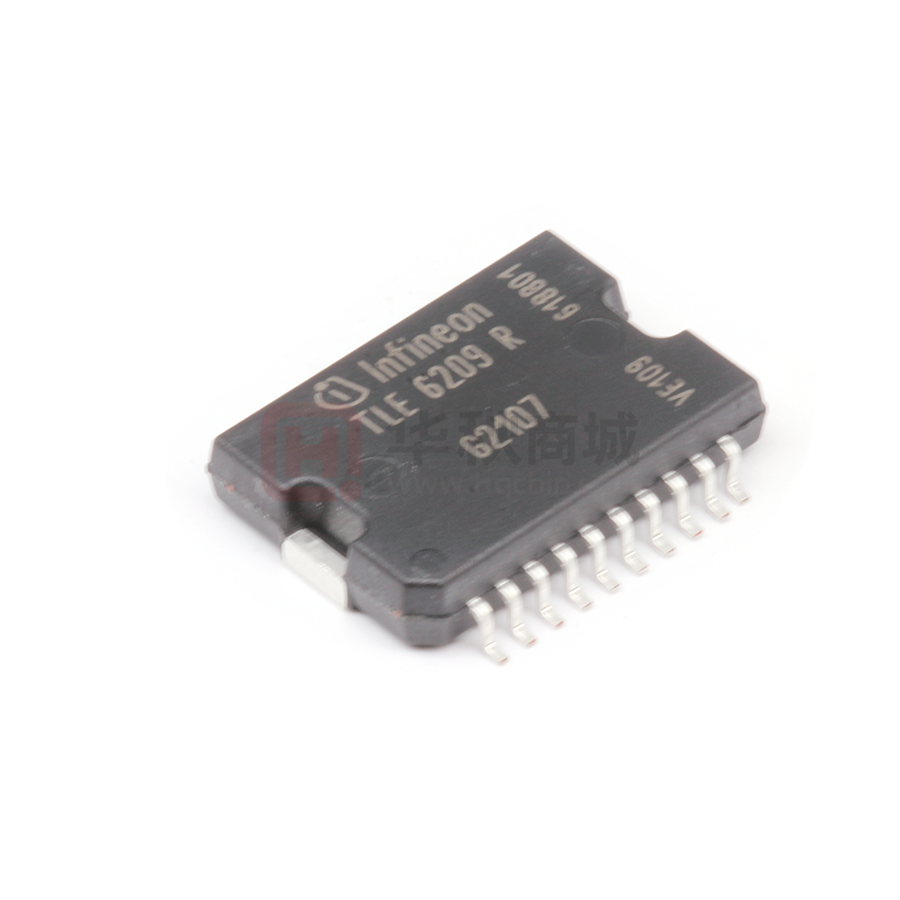
TLE 6209 R
Data Sheet
1
Overview
1.1
Features
•
•
•
•
•
•
•
•
•
•
•
•
•
•
•
•
•
•
Delivers up to 6 A continuous and 7 A peak current
Optimized for DC motor management applications
Very low RDS ON of typ. 150 mΩ @ 25 °C per switch
Operates at supply voltages of up to 40V
Overvoltage Protection against transients up to 45 V
Outputs fully short circuit protected
PG-DSO-20-37, -65
Standard SPI-Interface, daisy chain capability
Adjustable chopper current regulation of up to 7 A
Temperature monitor with prewarning, warning and shutdown
Over- and Undervoltage-Lockout
Open load detection
Detailed load failure diagnosis by SPI
Minimized power dissipation due to active free-wheeling
Low EMI due to voltage slope regulation
Very low current consumption (typ. 20 μA @ 25 °C) in stand-by (Inhibit) mode
Enhanced power PG-DSO-Package
Green Product (RoHS compliant)
AEC Qualified
Type
Package
TLE 6209 R
PG-DSO-20-37, -65
Functional Description
The TLE 6209 R is an integrated power H-Bridge with D-MOS output stages for driving
bidirectional loads such as DC-Motors. The design is based on Infineons Smart Power
Technology SPT which allows bipolar, CMOS and power D-MOS devices on the same
monolithic circuit.
Operation modes forward (cw), reverse (ccw) and brake are invoked by two control pins
PWM and DIR. Protection and a reliable diagnosis of overcurrent, openload, short-circuit
to ground, to the supply voltage or across the load are integrated. Detailed diagnostic
Data Sheet, Rev.3.2
1
2010-09-10
�TLE 6209 R
information is given via the 8 bit SPI status word. An integrated chopper current limitation
limits the current e.g. to reduce power dissipation during mechanical block of a DC
motor. Several device parameters can be set by the SPI control word. A three-level
temperature monitoring with prewarning, warning and shutdown is included for
controlled operation under critical power loss conditions. The full protection and
diagnosis capability make the device suitable especially for safety relevant applications,
e.g. in automotive ECUs.
1.2
Pin Configuration
(top view)
TLE 6209R
1
GND
GND
20
2
OUT 1
OUT 2
19
3
OUT 1
OUT 2
18
VS
VS
5
SCLK
DRV
6
SDI
VCC
15
7
SDO
PWM
14
8
CSN
DIR
13
9
INH
DIS
12
10
GND
GND
11
4
17
16
Metal slug,
connected to GND
Pin Definitions and Functions
VS
Power Supply Voltage
VCC
5 V Logic Supply
DRV
Input for Charge pump buffer
capacitor
GND
Ground
SDI
Serial Data Input
SDO
Serial Data Output
SCLK
Serial Clock Input
CSN
Chip-Select-Not Input
OUT
Power Output
–
–
PWM
PWM Input
DIR
Direction Input
DIS
Disable Input
INH
Inhibit
Data Sheet, Version 3.2
2
2010-09-10
�TLE 6209 R
1.2.1
Pin Definitions and Functions
Pin No. Symbol Function
1, 10,
11, 20
GND
Ground; internally connected to cooling tab (heat slug); to reduce
thermal resistance place cooling areas and thermal vias on PCB.
2,3
OUT1
Output 1; output of D-MOS half bridge 1; external connection
between pin 2 and pin 3 is necessary.
4,17
VS
Power supply; needs a blocking capacitor as close as possible to
GND; 47 μF electrolytic in parallel to 220 nF ceramic is
recommended; external connection between pin 4 and pin 17 is
necessary.
5
SCLK
Serial clock input; clocks the shiftregister; SCLK has an internal
active pull down and requires CMOS logic levels
6
SDI
Serial data input; receives serial data from the control device;
serial data transmitted to SDI is an 8 bit control word with the Least
Significant Bit (LSB) being transferred first; the input has an active
pull down and requires CMOS logic levels; SDI will accept data on
the falling edge of SCLK-signal; see Table 1 for input data protocol.
7
SDO
Serial-Data-Output; this tri-state output transfers diagnosis data to
the control device; the output will remain tri-stated unless the device
is selected by a low on Chip-Select-Not (CSN); SDO state changes
on the rising edge of SCLK; see Table 4 for diagnosis protocol.
8
CSN
Chip-Select-Not input; CSN is an active low input; serial
communication is enabled by pulling the CSN terminal low; CSN
input should only be transitioned when SCLK is low; CSN has an
internal active pull up and requires CMOS logic levels.
9
INH
Inhibit input; has an internal pull down; device is switched in
standby condition by pulling the INH terminal low.
12
DIS
Disable input; has an internal pull up; the output stages are
switched in tristate condition by pulling the DIS terminal high.
13
DIR
Direction input; has an internal pull down; TTL/CMOS compatible
input.
14
PWM
PWM input; has an internal pull down; TTL/CMOS compatible
input.
15
VCC
Logic supply voltage; needs a blocking capacitor as close as
possible to GND; 10 μF electrolytic in parallel to 220 nF ceramic is
recommended.
Data Sheet, Version 3.2
3
2010-09-10
�TLE 6209 R
1.2.1
Pin Definitions and Functions (cont’d)
Pin No. Symbol Function
16
DRV
Drive; Input for external charge pump capacitor CDRV
18,19
OUT2
Output 2; output of D-MOS half bridge 2; external connection
between pin 2 and pin 3 is necessary.
1.3
Functional Block Diagram
INH
DIS
CSN
SDI
SCLK
SDO
PWM
DIR
9
VCC
DRV
15
16
Bias
Charge
Pump
Inhibit
FaultDetect
12
8
6
5
7
S
P
I
14
VS
4,17
Driver
8 Bit
Logic
and
Latch
2,3
OUT 1
&
18,19
GateControl
OUT 2
Direct
Input
13
UV
OV
≥1
TSD
1,10,11,20
GND
Figure 1
Block Diagram
Data Sheet, Version 3.2
4
2010-09-10
�TLE 6209 R
2
Circuit Description
2.1
Serial Peripheral Interface (SPI)
The SPI is used for bidirectional communication with a control unit. The 8-bit
programming word or control word (see Table 1) is read in via the SDI serial data input,
and this is synchronized with the serial clock input SCLK. The status word appears
synchronously at the SDO serial data output (see Table 4).
The transmission cycle begins when the chip is selected with the chip-select-not (CSN)
input (H to L). When the CSN input changes from L to H, the word which has been read
into the shift register becomes the control word. The SDO output switches then to tristate
status, thereby releasing the SDO bus circuit for other uses. The SPI allows to parallel
multiple SPI devices by using multiple CSN lines. Due to the full duplex shift register, the
TLE 6209 R can also be used in daisy-chain configuration.
The settings made by the SPI control word become active at the end of the SPI
transmission and remain valid until a different control word is transmitted or a power on
reset occurs. At each SPI transmission, the diagnosis bits as currently valid in the error
logic are transmitted. The behavior of the diagnosis bits is described in Section 2.5.
Table 1
Input Data Protocol
Bit
7
Status Register Reset: H = reset
6
OVLO: H = on, L = off
5
not used
4
MSB of 2bit chopper-OFF-time
3
LSB of 2bit chopper-OFF-time
2
PWM Operation mode: H = Fast decay, L = Slow decay
1
MSB of 2 bit chopper current limit
0
LSB of 2 bit chopper current limit
Data Sheet, Version 3.2
5
2010-09-10
�TLE 6209 R
Table 2
Programmable Chopper Current Limit IL_xx
Bit 1
Bit 0
Current limit
0
0
0
1
1
0
1
1
IL_00
IL_01
IL_10
IL_11
Note: For actual values, see page 16
Table 3
Programmable Chopper OFF-time tOFF_xx
Bit 4
Bit 3
Chopper-OFF-time
tOFF_00
tOFF_01
tOFF_10
tOFF_11
0
0
0
1
1
0
1
1
Note: For actual values, see page 16
Table 4
Diagnosis Data Protocol
Bit
H = Error/L = no error
7
Power supply fail
6
not used, always H
5
Short to VS or across the load
4
Short to GND
3
Open load
2
MSB of Temperature Monitoring
1
LSB of Temperature Monitoring
0
Error-Flag
Table 5
Temperature Monitoring
Bit 2
Bit 1
Chip Temperature
0
0
Below Prewarning
0
1
Temperature Prewarning
Data Sheet, Version 3.2
6
2010-09-10
�TLE 6209 R
Table 5
Temperature Monitoring
Bit 2
Bit 1
Chip Temperature
1
0
Temperature Warning
1
1
Overtemperature Shutdown
2.2
Supply
2.2.1
Logic Supply Voltage, Power-On-Reset
The logic is supplied with 5 V by the VCC pin, separated from the power stage supply VS.
The advantage of this system is that information stored in the logic remains intact even
in the event of failures in the supply voltage VS. The power supply failure information can
be read out via the SPI. If VCC falls below typically 4.5 V, the logic is shut down, all
internally stored data is deleted and the Output Stages are switched to tristate. The IC is
restarted on rising VCC with a hysteresis of typically 80 mV
After this restart at increasing VCC, or if the device is activated after having been set into
inhibit mode (INH L to H), the IC is initialized by Power-On-Reset (POR). After POR, all
SPI control bits are set to L. This setting remains valid until first SPI communication. Also
the error bits are reset by POR.
2.2.2
Power Supply Voltage
The power stages are connected to the supply voltage VS. This voltage is monitored by
over voltage (OV) and under voltage (UV) comparators as described in Section 2.5.6.
The power supply voltage needs a blocking capacitor to GND.
2.3
Direct Inputs
2.3.1
Inhibit (sleep mode)
The INH input can be used to cut off the complete IC. By pulling the INH input to low, the
power stages are switched to tristate, and the current consumption is reduced to just a
few μA at both the VS and the VCC input. It also leads to the loss of any data stored. The
TLE 6209 R is reinitialized with POR if INH is put to high again. The pin has an internal
pull-down.
2.3.2
Disable
The DIS input can be used to disable the output stages. By pulling the DIS input to high
the power stages are switched to tristate, regardless of the signals at the DIR and PWM
inputs. The DIS input can be used as an emergency disable without resetting the SPI
data stored in the IC. It has an internal pull-up.
Data Sheet, Version 3.2
7
2010-09-10
�TLE 6209 R
2.3.3
Direction and PWM
The power stages are controlled by the direct inputs DIR and PWM as given in Table 6
and further illustrated in Figure 2. The DIR input gives the direction of output current,
while the PWM input controls whether the current is increased or reduced. The SPI
control bit 2 sets the decay mode, i.e. determines what happens if PWM = L. In pulsewidth modulated applications, this control scheme allows to supply the PWM-signal
always through the same port, using less controller resources.
Table 6
Functional Truth Table
DIR
PWM
MODE
(Bit 2)
OUT1
OUT2
Comments
0
1
0
(slow decay)
H
L
Motor turns clockwise
0
0
1
1
1
0
0
1
0
0
1
(fast decay)
H
H
Freewheel with slow decay
L
H
Motor turns counterclockwise
H
H
Freewheel with slow decay
H
L
Motor turns clockwise
L
H
Fast decay
1
1
L
H
Motor turns counterclockwise
1
0
H
L
Fast decay
Slow Decay
PWM = H
PWM = L
M
M
Fast Decay
Figure 2
PWM = H
PWM = L
M
M
DIR/PWM Control with Slow- and Fast Decay
Data Sheet, Version 3.2
8
2010-09-10
�TLE 6209 R
2.4
Power Stages
The output stages consist of a DMOS H-bridge built by two highside switches and two
lowside switches. Integrated circuits protect the outputs against overcurrent and
overtemperature if there is a short-circuit to ground or to the supply voltage or across the
load. Positive and negative voltage spikes, which occur when switching inductive loads,
are limited by integrated freewheeling diodes.
2.4.1
Charge Pump
To realize the fast switching times, the charge pump, which generates the voltage
necessary to switch on the n-channel D-MOS high-side switches, must be highly
efficient. It requires an external capacitor CDRV which is connected to VS and the charge
pump buffer input, DRV. It should be placed as close to the pins as possible.
2.4.2
Chopper Current Limitation
To limit the output current, a chopper current limitation is integrated as shown in
Figure 3. The current is measured by sense cells integrated in the low-side switches. As
soon the current limit IL is reached, the low-side switch is switched off for a fixed time
tOFF. IL and tOFF can be set by the SPI control bits 0,1, 3 and 4.
IOUT
current limit IL
off-time tOFF
time
Figure 3
2.4.3
Chopper current limitation
Active Freewheeling
When drivng inductive loads with PWM operation, the dissipated power can be
significantly reduced by activating the transistor located parallel to the internal
freewheeling diode. This is realized in the TLE 6209 R. When switching an output from
L to H, the high-side switch is turned on after a certain dead-time to avoid cross currents
flowing through the half bridge.
Data Sheet, Version 3.2
9
2010-09-10
�TLE 6209 R
2.5
Protection and Diagnosis
2.5.1
Short of Output to Ground
The high-side switches are protected against a short of the output to ground by an over
current shutdown. If a high-side switch is turned on and the current rises above the highside shutdown threshold ISDH for longer than the shutdown delay time tdOC, all output
transistors are turned off and bit 4 the SPI diagnosis word is set. During the delay time,
the current is limited to ISC (typically 20 A). The output stages stay off and the error bit
set until a status register reset (bit 7 of SPI control word) is received or a power-on reset
is performed.
2.5.2
Short of Output to VS
Due to the chopper current regulation, the low-side switches are protected against a
short to the supply voltage. To detect the short, the first time the current limit is reached,
the off-command for the low-side switch is blanked out for 10 μs. If the current rises
above the low-side shutdown threshold ISDL during this time, all output transistors are
turned off and bit 5 in the SPI diagnosis word is set. The value of the shutdown threshold
depends on the current limit that is set via the SPI. The shutdown threshold is 1 A higher
than the current limit. The output stages stay off and the error bit set until a status register
reset (bit 7 of SPI control word) is received or a power-on reset is performed.
2.5.3
Short Across the Load
The short circuit protection circuits of the high- and low-side switches work
independently of each other. In most cases, a short across the load will be detected as
a short to VS because of the longer filter time in the high-side switches tdOC and the higher
shutdown threshold ISDH.
2.5.4
Open Load
If the current through the low side transistor is lower than the reference current IdOL in
ON-state (PWM = H), a timer is started. After a filter time tdOC an open load failure will be
recognized and the status bit 3 is set. If the current exceeds the reference current IdOL
the open load timer is reset. If the H-bridge is switched to OFF-state (PWM = L) the timer
is stopped but not reset. The timer continues if the H-bridge is switched to ON-state
again. There is no reset of the open load timer if the direction is changed using the DIR
input in open load condition. The open load error bit is latched and can be reset by the
status register reset bit 7 of the SPI control word or a POR.
2.5.5
Temperature Monitoring
Temperature sensors are integrated in the power stages. The temperature monitoring
circuit compares the measured temperature to the prewarning, warning and shutdown
Data Sheet, Version 3.2
10
2010-09-10
�TLE 6209 R
thresholds. As soon as a threshold is reached, the according status bits are set in the
SPI diagnosis word (c.f. Table 5). If the overtemperature shutdown threshold is reached,
the output stages are turned off. The temperature monitoring messages and the over
temperature shutdown are latched and can be reset by the status register reset bit 7 of
the SPI control word or a POR.
2.5.6
Power Supply Fail
The power supply Voltage is monitored for over- and under voltage lockout:
• Under Voltage Lockout
If the supply voltage VS drops below the switch off voltage VUV OFF, all output
transistors are switched off and the power supply fail bit (bit 7 of the SPI diagnosis
word) is set. If VS rises again and reaches the switch on voltage VUV ON, the power
stages are restarted. The error bit, however, is latched and has to be reset by the
status register reset bit 7 of the SPI control word.
• Over Voltage Lockout
If the supply voltage VS rises above the switch off voltage VOV OFF, all output transistors
are switched off and the power supply fail bit (bit 7 of the SPI diagnosis word) is set.
If VS falls again and reaches the switch on voltage VOV ON, the power stages are
restarted. The error bit, however, is latched and has to be reset by the status register
reset bit 7 of the SPI control word.
The OVLO is only active if control bit 6 is H. If the bit is low, the OVLO is deactivated.
2.5.7
Error Flag
Bit 0 of the SPI diagnosis word is an OR of the status bits 1 to 7. It can be read out without
full SPI communication as described in Figure 8.
Data Sheet, Version 3.2
11
2010-09-10
�TLE 6209 R
3
Characteristics
3.1
Absolute Maximum Ratings
Parameter
Symbol
Limit Values
Unit
Remarks
–
min.
max.
VS
VS
VCC
VI
– 0.3
40
V
–1
45
V
t < 0.5 s; IS > – 2 A
– 0.3
5.5
V
0 V < VS < 40 V
– 0.3
5.5
V
0 V < VS < 40 V
0 V < VCC < 5.5 V
Logic output voltage
(SDO)
VO
– 0.3
5.5
V
0 V < VS < 40 V
0 V < VCC < 5.5 V
Output voltage
(OUT1, OUT2)
VOUT
– 0.3 V VS +
1,5V
–
0 V < VS < 40 V
Charge pump buffer voltage
(DRV)
VDRV
VS –
0.3 V
VS +
15 V
–
0 V < VS < 40 V
IOUT
IOUT
–
–
A
–
–
A
internally limited,
see page 16 and
page 17.
Tj
Tstg
– 40
150
°C
–
– 50
150
°C
–
Voltages
Supply voltage
Supply voltage
Logic supply voltage
Logic input voltages
(SDI, SCLK, CSN, INH,
DIS, PWM, DIR)
Currents
Output current (cont.)
Output current (peak)
Temperatures
Junction temperature
Storage temperature
Note: Maximum ratings are absolute ratings; exceeding any one of these values may
cause irreversible damage to the integrated circuit.
Data Sheet, Version 3.2
12
2010-09-10
�TLE 6209 R
3.2
Operating Range
Parameter
Symbol
Limit Values
min.
Unit
Remarks
max.
Supply voltage
VS
VUV OFF 40
V
After VS rising
above VUV ON
Supply voltage slew rate
dVS /dt
–10
10
V/μs
–
Logic supply voltage
VCC
VS
VS
VI
4.75
5.50
V
– 0.3
Outputs in tristate
– 0.3
VUV ON V
VUV OFF V
VCC
V
fCLK
Tj
–
2
MHz
–
– 40
150
°C
–
Junction pin
RthjC
–
1.5
K/W
measured to
pin 1, 10, 11, 20
Junction ambient
RthjA
–
50
K/W
–
Supply voltage increasing
Supply voltage decreasing
Logic input voltage (SDI,
SCLK, CSN, INH)
SPI clock frequency
Junction temperature
– 0.3
–
Outputs in tristate
–
Thermal Resistances
Data Sheet, Version 3.2
13
2010-09-10
�TLE 6209 R
3.3
Electrical Characteristics
8 V < VS < 40 V; 4.75 V < VCC < 5.25 V; INH = High; all outputs open;
– 40 °C < Tj < 150 °C; unless otherwise specified
Parameter
Symbol
Limit Values
min.
typ.
max.
Unit Test Conditions
Current Consumption
Quiescent current
IS
–
–
50
μA
INH = Low;
VS = 13.2 V
Quiescent current
IS
–
10
30
μA
INH = Low;
VS = 13.2 V;
Tj = 25 °C
Logic-Supply current
ICC
ICC
IS
–
–
20
μA
INH = Low
–
2.0
4.0
mA
–
–
2.8
5.0
mA
–
–
5.4
5.7
V
4.4
4.9
5.2
V
0.2
0.5
–
V
34
37
40
V
28
32
36
V
–
5.0
–
V
VS increasing
VS decreasing
VUV ON – VUV OFF
VS increasing
VS decreasing
VOV OFF – VOV ON
Logic-Supply current
Supply current
Over- and Under-Voltage Lockout
UV-Switch-ON voltage
UV-Switch-OFF voltage
UV-ON/OFF-Hysteresis
OV-Switch-OFF voltage
OV-Switch-ON voltage
OV-ON/OFF-Hysteresis
Data Sheet, Version 3.2
VUV ON
VUV OFF
VUV HY
VOV OFF
VOV ON
VOV HY
14
2010-09-10
�TLE 6209 R
3.3
Electrical Characteristics (cont’d)
8 V < VS < 40 V; 4.75 V < VCC < 5.25 V; INH = High; all outputs open;
– 40 °C < Tj < 150 °C; unless otherwise specified
Parameter
Symbol
Limit Values
min.
Unit Test Conditions
typ.
max.
140
170
mΩ
5.2 V < VS < 40 V
Tj = 25 °C;
CDRV = 33 nF
–
280
mΩ
5.2 V < VS < 40 V
CDRV = 33 nF
130
160
mΩ
5.2 V < VS < 40 V
Tj = 25 °C;
CDRV = 33 nF
–
270
mΩ
5.2 V < VS < 40 V
CDRV = 33 nF
–
1.0
1.5
V
–
1.0
1.5
V
IF = 3 A
IF = 3 A
Outputs OUT1-2
Static Drain-Source-On Resistance
Source (High-Side)
IOUT = – 3 A
Sink (Low-Side)
IOUT = 3 A
RDS ON H –
RDS ON L –
Clamp Diodes Forward Voltage
Upper
Lower
Data Sheet, Version 3.2
VFU
VFL
15
2010-09-10
�TLE 6209 R
3.3
Electrical Characteristics (cont’d)
8 V < VS < 40 V; 4.75 V < VCC < 5.25 V; INH = High; all outputs open;
– 40 °C < Tj < 150 °C; unless otherwise specified
Parameter
Symbol
Limit Values
Unit Test Conditions
min.
typ.
max.
IOCD
tdOC
30
–
130
mA
–
2
–
8
ms
–
Current limit
IL_00
3.4
4
4.6
A
Bit 0 = L;
Bit 1 = L;
Current limit
IL_01
4.25
5
5.75
A
Bit 0 = H;
Bit 1 = L;
Current limit
IL_10
5.1
6
6.9
A
Bit 0 = L;
Bit 1 = H;
Current limit
IL_11
5.95
7
8.05
A
Bit 0 = H;
Bit 1 = H;
0.5
1.0
1.5
A
ΔISDL = ISDL - IL
Open Circuit/Underload Detection
Detection current
Delay time
Current Limits
Low-Side Switch Overcurrent
Shutdown Threshold
ΔISDL
Note: low-side shutdown threshold is guaranteed by design
Switch-OFF Time during Current Limitation (Chopper OFF-Time)
OFF-time
tOFF_00
16
24
28
μs
Bit 3 = L;
Bit 4 = L;
OFF-time
tOFF_01
32
43
51
μs
Bit 3 = H;
Bit 4 = L;
OFF-time
tOFF_10
48
62
74
μs
Bit 3 = L;
Bit 4 = H;
OFF-time
tOFF_11
64
80
96
μs
Bit 3 = H;
Bit 4 = H;
Data Sheet, Version 3.2
16
2010-09-10
�TLE 6209 R
3.3
Electrical Characteristics (cont’d)
8 V < VS < 40 V; 4.75 V < VCC < 5.25 V; INH = High; all outputs open;
– 40 °C < Tj < 150 °C; unless otherwise specified
Parameter
Symbol
Limit Values
min.
typ.
max.
Unit Test Conditions
High-Side Switch Overcurrent
High-side shutdown
threshold
ISDH
8
12
18
A
–
Shutdown delay time
tdSD
ISC
15
25
40
μs
–
–
–
25
A
during tdSD
Short circuit current
Note: For short circuit current definition, see Figure 5. Short circuit current is
guaranteed by design
Leakage Current / Output Current in Tristate
Source-Output-Stage
Sink-Output-Stage
IQLH
IQLL
– 120 – 50
–
μA
–
1
mA
VOUT = 0 V
VOUT = VS
VS = 13.2 V,
0.5
Output Delay Times (device not in stand-by for t > 1 ms)
High-side ON
High-side OFF
Low-side ON
Low-side OFF
td ON H
td OFF H
td ON L
td OFF L
–
4
10
μs
–
0.6
1
μs
–
2
3.5
μs
–
2.5
4
μs
Resistive load of
12 Ω
Output Switching Times (device not in stand-by for t > 1 ms)
High-side switch rise time
High-side switch fall time
Low-side switch rise time
Low-side switch fall time
tRISE H
tFALL H
tRISE L
tFALL L
–
1.8
3.5
μs
–
0.2
0.8
μs
2
6.5
11
μs
2
4.3
6.5
μs
VS = 13.2 V,
Resistive load of
12 Ω
Note: For switching time definitions, see Figure 6.
Data Sheet, Version 3.2
17
2010-09-10
�TLE 6209 R
3.3
Electrical Characteristics (cont’d)
8 V < VS < 40 V; 4.75 V < VCC < 5.25 V; INH = High; all outputs open;
– 40 °C < Tj < 150 °C; unless otherwise specified
Parameter
Symbol
Limit Values
min.
typ.
max.
–
–
0.7
0.2
–
50
300
10
–
H-input voltage threshold
L-input voltage threshold
Unit Test Conditions
Inhibit Input
VIINHH
L-input voltage threshold
VIINHL
Hysteresis of input voltage VIINHHY
Pull down current (low)
IIINHL
Pull down current (high)
IIINHH
H-input voltage threshold
–
–
VCC
VCC
500
mV
–
25
50
μA
–
80
μA
VIINH = 0.2 × VCC
VIINH = 0.7 × VCC
–
–
0.7
–
–
VCC
VCC
–
0.2
50
300
500
mV
–
– 50
– 25
– 10
μA
– 50
–
–
μA
VIDIS = 0.7 × VCC
VIDIS = 0.2 × VCC
–
–
0.7
–
0.2
–
–
VCC
VCC
50
300
500
mV
–
10
25
50
μA
–
–
50
μA
VI= 0.2 × VCC
VI= 0.7 × VCC
–
Disable Input
VIDISH
VIDISL
Hysteresis of input voltage VIDISHY
Pull up current (high)
IIDISH
Pull up current (low)
IIDISL
–
Direction/PWM Input
VIH
L-input voltage threshold
VIL
Hysteresis of input voltage VIHY
Pull down current (low)
II
Pull down current (high)
II
H-input voltage threshold
Data Sheet, Version 3.2
18
–
2010-09-10
�TLE 6209 R
3.3
Electrical Characteristics (cont’d)
8 V < VS < 40 V; 4.75 V < VCC < 5.25 V; INH = High; all outputs open;
– 40 °C < Tj < 150 °C; unless otherwise specified
Parameter
Symbol
Limit Values
min.
typ.
Unit Test Conditions
max.
SPI-Interface
Delay Time from Stand-by to Data In/Power on Reset
–
–
100
μs
–
–
–
0.7
–
0.2
–
–
VCC
VCC
50
300
500
mV
–
– 50
– 25
– 10
μA
VCSN = 0.7 × VCC
– 50
–
–
μA
VCSN = 0.2 × VCC
Pull down current at pin SDI IISDIL
and SCLK (low)
(IISCLKL)
10
25
50
μA
Pull down current at pin SDI IISDIH
and SCLK (high)
(IISCLKH)
–
–
50
μA
–
10
15
pF
VSDI (VSCLK) = 0.2 ×
VCC
VSDI (VSCLK) = 0.7 ×
VCC
0 V < VCC < 5.25 V
Setup time
tset
Logic Inputs SDI, SCLK and CSN
VIH
L-input voltage threshold
VIL
Hysteresis of input voltage VIHY
Pull up current at pin CSN IICSNH
H-input voltage threshold
(high)
Pull up current at pin CSN
(low)
Input capacitance
at pin CSN, SDI or SCLK
IICSNL
CI
–
Note: Input capacitances are guaranteed by design.
Data Sheet, Version 3.2
19
2010-09-10
�TLE 6209 R
3.3
Electrical Characteristics (cont’d)
8 V < VS < 40 V; 4.75 V < VCC < 5.25 V; INH = High; all outputs open;
– 40 °C < Tj < 150 °C; unless otherwise specified
Parameter
Symbol
Limit Values
Unit Test Conditions
min.
typ.
max.
VSDOH
VCC
VCC
–
V
ISDOH = 1 mA
–
0.25
0.4
V
Tri-state leakage current
VSDOL
ISDOLK
– 10
–
10
μA
Tri-state input capacitance
CSDO
–
10
15
pF
ISDOL = – 1.6 mA
VCSN = VCC
0 V < VSDO < VCC
VCSN = VCC
0 V < VCC < 5.25 V
Logic Output SDO
H-output voltage level
L-output voltage level
–1.0
–0.85
Note: Input capacitances are guaranteed by design.
Data Sheet, Version 3.2
20
2010-09-10
�TLE 6209 R
3.3
Electrical Characteristics (cont’d)
8 V < VS < 40 V; 4.75 V < VCC < 5.25 V; INH = High; all outputs open;
– 40 °C < Tj < 150 °C; unless otherwise specified
Parameter
Symbol
Limit Values
Unit Test Conditions
min.
typ.
max.
tPSCLK
tSCLKH
tSCLKL
tbef
500
–
–
ns
–
250
–
–
ns
–
250
–
–
ns
–
250
–
–
ns
–
tlead
tlag
tbeh
tSDISU
tSDIHO
trSIN
250
–
–
ns
–
250
–
–
ns
–
250
–
–
ns
–
125
–
–
ns
–
125
–
–
ns
–
–
–
100
ns
–
–
–
100
ns
–
–
25
50
ns
–
25
50
ns
CL = 100 pF
CL = 100 pF
–
–
125
ns
low impedance
–
–
125
ns
high impedance
–
50
125
ns
VDO < 0.2 VCC;
VDO > 0.7 VCC;
CL = 100 pF
Serial Data Input Timing
Serial Clock period
Serial Clock high time
Serial Clock low time
Serial Clock low
before CSN low
CSN setup time
SCLK setup time
Clock low after CSN high
SDI setup time
SDI hold time
Input signal rise time
at pin SDI, SCLK and CSN
Input signal fall time
tfSIN
at pin SDI, SCLK and CSN
Serial Data Output Timing
SDO rise time
SDO fall time
SDO enable time
SDO disable time
SDO valid time
Data Sheet, Version 3.2
trSDO
tfSDO
tENSDO
tDISSDO
tVASDO
21
2010-09-10
�TLE 6209 R
3.3
Electrical Characteristics (cont’d)
8 V < VS < 40 V; 4.75 V < VCC < 5.25 V; INH = High; all outputs open;
– 40 °C < Tj < 150 °C; unless otherwise specified
Parameter
Symbol
Limit Values
min.
typ.
Unit Test Conditions
max.
Thermal Prewarning, Warning and Shutdown
Thermal prewarning
junction temperature
TjPW
120
140
160
°C
–
Temperature prewarning
hysteresis
ΔT
–
20
–
K
–
Thermal warning junction
temperature
TjW
140
160
180
°C
–
Temperature prewarning
hysteresis
ΔT
–
20
–
K
–
160
180
200
°C
–
Thermal shutdown junction TjSD
temperature
Temperature shutdown
hysteresis
ΔT
–
20
–
K
–
Ratio of W to PW
temperature
TjW /
TjPW
1.07
1.14
–
–
–
Ratio of SD to W
temperature
TjSD /
TjW
1.06
1.13
–
–
–
Note: Temperature thresholds are guaranteed by design.
Data Sheet, Version 3.2
22
2010-09-10
�TLE 6209 R
4
Diagrams
V
13.2V
VOUT
9V
9V
0
tOFF_xx
IOUT
Figure 4
Switch-OFF time during current limitation (chopper OFF-time)
Vs
V
Vs
5V
PWM
0
OUT
tdSD
IOUT
ISDH
ISC
GND
Figure 5
Short circuit of high-side switch to GND
Data Sheet, Version 3.2
23
2010-09-10
�TLE 6209 R
V
PWM
Input
5
50%
50%
0
tRISE
tFALL
100%
90%
90%
VOUT
10%
10%
td1
td2
DIR = L / H => VOUT = VOUT 1/2
Resistive load to Vs =>
tRISE = tRISE L, tFALL = tFALL L
td1 = td OFF L, td2 = td ON L
Figure 6
Resistive load to GND =>
tRISE = tRISE H, tFALL = tFALL H
td1 = td ON H, td2 = td OFF H
Output Delay and Switching Time Definitions
CSN High to Low & rising edge of SCLK: SDO is enabled. Status information is transfered to Output Shift Register
CSN
time
CSN Low to High: Data from Shift-Register is transfered to Output Driver Logic
SCLK
0
2
1
4
3
5
6
7
0
new Data
actual Data
0
SDI
1
2
3
5
4
6
0
+
7
SDI: Data will be accepted on the falling edge of CLK-Signal
actual Status
previous Status
SDO
_
0
1
_
_
2
_
3
_
4
_
5
_
6
_
7
0
SDO: State will change on the rising edge of CLK-Signal
old Data
Figure 7
actual Data
Standard Data Transfer Timing
Data Sheet, Version 3.2
24
2010-09-10
�TLE 6209 R
CSN High to Low & SCLK stays Low: Status information of Data Bit 0 ( Error Flag )
is transfered to SDO
CSN
time
SCLK
SDI
SDI: Data is not accepted
SDO tristate
_
0
tristate
SDO: Status information of Data Bit 0 ( Error-Flag ) will stay as long as CSN is low
Figure 8
Timing for Error Detection Only
0.7 VCC
CSN
0.2 VCC
tSCLKH
0.7 VCC
SCLK
0.2 VCC
tlead
tbef
tSCLKL
tlag
tSDISU
tbeh
tSDIHO
SDI
Don´t care
Don´t
care
Valid
0.7 VCC
Valid
Don´t care
0.2 VCC
Figure 9
SPI-Input Timing
Data Sheet, Version 3.2
25
2010-09-10
�TLE 6209 R
trSIN
tfSIN
0.7 VCC
SCLK
50 %
0.2 VCC
trSDO
0.7 VCC
SDO
( low to high )
0.2 VCC
tVASDO
tfSDO
0.7 VCC
SDO
Figure 10
( high to low )
0.2 VCC
DO Valid Data Delay Time and Valid Time
tfSIN
trSIN
0.7 VCC
CSN
50 %
0.2 VCC
tENSDO
tDISSDO
10 kΩ
Pullup
to VCC
SDO
tENSDO
tDISSDO
10 kΩ
Pulldown 50 %
to GND
SDO
Figure 11
50 %
SDO Enable and Disable Time
Data Sheet, Version 3.2
26
2010-09-10
�TLE 6209 R
5
Application
Watchdog
Reset
Q
TLE
4278G
Z39
D
CQ
22µF
Vbat
I
CD
10nF
100µF
100nF
GND
CDRV
WD R
VCC
VCC
DRV
15
MicroController
for
EMS/ETC
Function
INH
9
DIS
12
CSN
SDI
SCLK
SDO
PWM
DIR
VS
33nF
16
Bias
Charge
Pump
Inhibit
FaultDetect
4,17
8
2,3
6
S
5
P
7
I
OUT 1
Driver
8 Bit
Logic
and
Latch
&
18,19
Gate-Control
OUT 2
M
14
Direct
Input
13
UV
GND
≥1
OV
Micro-Controller
for
Evaluation Process Monitoring
TSD
GND
GND
Figure 12
Application Circuit
Data Sheet, Version 3.2
27
2010-09-10
�TLE 6209 R
6
Package Outlines
-0.027
B
5˚ ±3˚
0.25 +0.0
11 ±0.15 1)
2.8
1.3
1.2 -0.3
3.5 max.
0 +0.15
3.25 ±0.1
PG-DSO-20-37, -65
(Plastic Dual Small Outline Package)
15.74 ±0.1
1.27
Index Marking
6.3
0.1
0.4 +0.13
0.25
M
20
11
1
1 x 45˚
10
A 20x
14.2 ±0.3
Heatsink
0.95 ±0.15
0.25
M
B
15.9 ±0.15 1)
A
1) Does not include plastic or metal protrusion of 0.15 max. per side
GPS05791
Green Product (RoHS compliant)
To meet the world-wide customer requirements for environmentally friendly products
and to be compliant with government regulations the device is available as a green
product. Green products are RoHS-Compliant (i.e Pb-free finish on leads and suitable
for Pb-free soldering according to IPC/JEDEC J-STD-020).
You can find all of our packages, sorts of packing and others in our
Infineon Internet Page “Products”: http://www.infineon.com/products.
Dimensions in mm
SMD = Surface Mounted Device
Data Sheet, Version 3.2
28
2010-09-10
�TLE 6209 R
7
Revision History
Version
Date
Rev. 3.1
2007-08-01 RoHS-compliant version of the TLE 6209 R
• All pages: Infineon logo updated
• Page 1:
“AEC qualified” and “RoHS” logo added, “Green Product
(RoHS compliant)” and “AEC qualified” statement added to
feature list, package names changed to RoHS compliant
versions, package pictures updated, ordering codes
removed
• Page 28:
Package name changed to RoHS compliant version,
“Green Product” description added
• Revision History added
• Legal Disclaimer added
Rev. 3.2
2010-09-10 Package name updated
Data Sheet, Version 3.2
Changes
29
2010-09-10
�Edition 2010-09-10
Published by
Infineon Technologies AG
81726 Munich, Germany
© 9/10/10 Infineon Technologies AG
All Rights Reserved.
Legal Disclaimer
The information given in this document shall in no event be regarded as a guarantee of conditions or
characteristics. With respect to any examples or hints given herein, any typical values stated herein and/or any
information regarding the application of the device, Infineon Technologies hereby disclaims any and all warranties
and liabilities of any kind, including without limitation, warranties of non-infringement of intellectual property rights
of any third party.
Information
For further information on technology, delivery terms and conditions and prices, please contact the nearest
Infineon Technologies Office (www.infineon.com).
Warnings
Due to technical requirements, components may contain dangerous substances. For information on the types in
question, please contact the nearest Infineon Technologies Office.
Infineon Technologies components may be used in life-support devices or systems only with the express written
approval of Infineon Technologies, if a failure of such components can reasonably be expected to cause the failure
of that life-support device or system or to affect the safety or effectiveness of that device or system. Life support
devices or systems are intended to be implanted in the human body or to support and/or maintain and sustain
and/or protect human life. If they fail, it is reasonable to assume that the health of the user or other persons may
be endangered.
�


 工商网监
湘ICP备2023018690号
工商网监
湘ICP备2023018690号

