TLE7181EM
H-Bridge and Dual Half Bridge Driver IC
Features
•
PWM/DIR-interface drives 4 N-Channel Power MOSFETs
•
Unlimited D.C. switch on time of low and high-side MOSFETs
•
0 … 95% at 20 kHz & 100% duty cycle of high-side MOSFETs
•
0 … 100% duty cycle of low-side MOSFETs
•
Additional output to drive a reverse polarity protection N-MOSFET
•
Current sense OPAMP
•
Low quiescent current mode
•
Internal shoot through protection
•
Adjustable dead time
•
1-bit diagnosis / ERR
•
Overcurrent warning based on current sense OPAMP with fixed warning level
•
Analog adjustable short circuit protection levels via SCDL pin with open pin detection
•
Overtemperature warning
•
Overvoltage warning
•
Undervoltage warning and shutdown
•
Green Product (RoHS compliant)
•
AEC Qualified
Potential applications
General automotive applications.
Product validation
Qualified for automotive applications. Product validation according to AEC-Q100/101.
Description
Typical applications are fans, pumps and electric power steering. The TLE7181EM is designed for a 12 V power
net.
Datasheet
www.infineon.com
1
Rev 1.2
2019-03-14
�TLE7181EM
H-Bridge and Dual Half Bridge Driver IC
Table 1
Product summary
Parameter
Symbol
Values
Specified operating voltage
VSOP
7.0 V … 34 V
Junction temperature
Tj
-40°C … 150°C
Maximum output source resistance
RSou
13.5 Ω
Maximum output sink resistance
RSink
9Ω
Maximum quiescent current1)
IQVS
8 µA
1) Typical value at Tj = 25°C
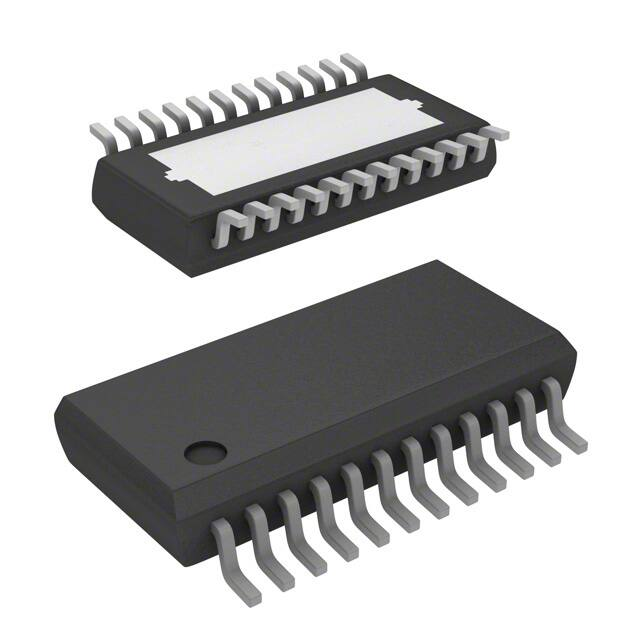
Type
Package
Marking
TLE7181EM
PG-SSOP-24
TLE7181EM
Datasheet
2
Rev 1.2
2019-03-14
�TLE7181EM
H-Bridge and Dual Half Bridge Driver IC
Table of Contents
Features . . . . . . . . . . . . . . . . . . . . . . . . . . . . . . . . . . . . . . . . . . . . . . . . . . . . . . . . . . . . . . . . . . . . . . . . 1
Potential applications . . . . . . . . . . . . . . . . . . . . . . . . . . . . . . . . . . . . . . . . . . . . . . . . . . . . . . . . . . . . . 1
Product validation . . . . . . . . . . . . . . . . . . . . . . . . . . . . . . . . . . . . . . . . . . . . . . . . . . . . . . . . . . . . . . . . 1
Description . . . . . . . . . . . . . . . . . . . . . . . . . . . . . . . . . . . . . . . . . . . . . . . . . . . . . . . . . . . . . . . . . . . . . . 1
Table of Contents . . . . . . . . . . . . . . . . . . . . . . . . . . . . . . . . . . . . . . . . . . . . . . . . . . . . . . . . . . . . . . . . . 3
1
Block diagram . . . . . . . . . . . . . . . . . . . . . . . . . . . . . . . . . . . . . . . . . . . . . . . . . . . . . . . . . . . . . . . . . . . 5
2
2.1
2.2
Pin configuration . . . . . . . . . . . . . . . . . . . . . . . . . . . . . . . . . . . . . . . . . . . . . . . . . . . . . . . . . . . . . . . . . 6
Pin assignment . . . . . . . . . . . . . . . . . . . . . . . . . . . . . . . . . . . . . . . . . . . . . . . . . . . . . . . . . . . . . . . . . . . . . . . . . . . 6
Pin definitions and functions . . . . . . . . . . . . . . . . . . . . . . . . . . . . . . . . . . . . . . . . . . . . . . . . . . . . . . . . . . . . . . 6
3
3.1
3.2
3.3
3.3.1
General product characteristics . . . . . . . . . . . . . . . . . . . . . . . . . . . . . . . . . . . . . . . . . . . . . . . . . . . . 8
Absolute maximum ratings . . . . . . . . . . . . . . . . . . . . . . . . . . . . . . . . . . . . . . . . . . . . . . . . . . . . . . . . . . . . . . . . 8
Functional range . . . . . . . . . . . . . . . . . . . . . . . . . . . . . . . . . . . . . . . . . . . . . . . . . . . . . . . . . . . . . . . . . . . . . . . . . 9
Thermal resistance . . . . . . . . . . . . . . . . . . . . . . . . . . . . . . . . . . . . . . . . . . . . . . . . . . . . . . . . . . . . . . . . . . . . . . 10
Default state of inputs . . . . . . . . . . . . . . . . . . . . . . . . . . . . . . . . . . . . . . . . . . . . . . . . . . . . . . . . . . . . . . . . . . 11
4
4.1
4.1.1
4.1.2
4.1.3
4.1.4
4.1.5
4.1.6
4.1.7
4.1.8
4.2
4.3
4.3.1
4.3.2
4.3.3
4.3.4
4.3.5
4.3.6
4.3.7
4.3.8
4.3.9
4.3.10
4.3.11
4.4
4.4.1
Description and electrical characteristics . . . . . . . . . . . . . . . . . . . . . . . . . . . . . . . . . . . . . . . . . . .
MOSFET driver . . . . . . . . . . . . . . . . . . . . . . . . . . . . . . . . . . . . . . . . . . . . . . . . . . . . . . . . . . . . . . . . . . . . . . . . . .
Driving MOSFET output stages . . . . . . . . . . . . . . . . . . . . . . . . . . . . . . . . . . . . . . . . . . . . . . . . . . . . . . . . . .
MOSFET output stages . . . . . . . . . . . . . . . . . . . . . . . . . . . . . . . . . . . . . . . . . . . . . . . . . . . . . . . . . . . . . . . . .
Dead time . . . . . . . . . . . . . . . . . . . . . . . . . . . . . . . . . . . . . . . . . . . . . . . . . . . . . . . . . . . . . . . . . . . . . . . . . . . .
Bootstrap principle . . . . . . . . . . . . . . . . . . . . . . . . . . . . . . . . . . . . . . . . . . . . . . . . . . . . . . . . . . . . . . . . . . . .
100% D.C. charge pumps . . . . . . . . . . . . . . . . . . . . . . . . . . . . . . . . . . . . . . . . . . . . . . . . . . . . . . . . . . . . . . .
Reverse polarity protection of motor bridge . . . . . . . . . . . . . . . . . . . . . . . . . . . . . . . . . . . . . . . . . . . . . .
Sleep mode . . . . . . . . . . . . . . . . . . . . . . . . . . . . . . . . . . . . . . . . . . . . . . . . . . . . . . . . . . . . . . . . . . . . . . . . . . .
Wake up . . . . . . . . . . . . . . . . . . . . . . . . . . . . . . . . . . . . . . . . . . . . . . . . . . . . . . . . . . . . . . . . . . . . . . . . . . . . . .
Electrical characteristics . . . . . . . . . . . . . . . . . . . . . . . . . . . . . . . . . . . . . . . . . . . . . . . . . . . . . . . . . . . . . . . . .
Protection and diagnostic functions . . . . . . . . . . . . . . . . . . . . . . . . . . . . . . . . . . . . . . . . . . . . . . . . . . . . . . .
State diagram of different operation modes . . . . . . . . . . . . . . . . . . . . . . . . . . . . . . . . . . . . . . . . . . . . . .
Short circuit protection . . . . . . . . . . . . . . . . . . . . . . . . . . . . . . . . . . . . . . . . . . . . . . . . . . . . . . . . . . . . . . . . .
SCDL pin open detection . . . . . . . . . . . . . . . . . . . . . . . . . . . . . . . . . . . . . . . . . . . . . . . . . . . . . . . . . . . . . . .
Vs and VDH overvoltage warning . . . . . . . . . . . . . . . . . . . . . . . . . . . . . . . . . . . . . . . . . . . . . . . . . . . . . . . .
VS undervoltage shutdown . . . . . . . . . . . . . . . . . . . . . . . . . . . . . . . . . . . . . . . . . . . . . . . . . . . . . . . . . . . . .
VREG undervoltage warning . . . . . . . . . . . . . . . . . . . . . . . . . . . . . . . . . . . . . . . . . . . . . . . . . . . . . . . . . . . .
Overtemperature warning . . . . . . . . . . . . . . . . . . . . . . . . . . . . . . . . . . . . . . . . . . . . . . . . . . . . . . . . . . . . . .
Overcurrent warning . . . . . . . . . . . . . . . . . . . . . . . . . . . . . . . . . . . . . . . . . . . . . . . . . . . . . . . . . . . . . . . . . . .
Passive Gxx clamping . . . . . . . . . . . . . . . . . . . . . . . . . . . . . . . . . . . . . . . . . . . . . . . . . . . . . . . . . . . . . . . . . .
ERR pin . . . . . . . . . . . . . . . . . . . . . . . . . . . . . . . . . . . . . . . . . . . . . . . . . . . . . . . . . . . . . . . . . . . . . . . . . . . . . . .
Electrical characteristics . . . . . . . . . . . . . . . . . . . . . . . . . . . . . . . . . . . . . . . . . . . . . . . . . . . . . . . . . . . . . . . .
Shunt signal conditioning . . . . . . . . . . . . . . . . . . . . . . . . . . . . . . . . . . . . . . . . . . . . . . . . . . . . . . . . . . . . . . . .
Electrical characteristics . . . . . . . . . . . . . . . . . . . . . . . . . . . . . . . . . . . . . . . . . . . . . . . . . . . . . . . . . . . . . . . .
5
5.1
5.2
Application information . . . . . . . . . . . . . . . . . . . . . . . . . . . . . . . . . . . . . . . . . . . . . . . . . . . . . . . . . . 27
Layout guidelines . . . . . . . . . . . . . . . . . . . . . . . . . . . . . . . . . . . . . . . . . . . . . . . . . . . . . . . . . . . . . . . . . . . . . . . . 28
Further application information . . . . . . . . . . . . . . . . . . . . . . . . . . . . . . . . . . . . . . . . . . . . . . . . . . . . . . . . . . . 28
6
Package information . . . . . . . . . . . . . . . . . . . . . . . . . . . . . . . . . . . . . . . . . . . . . . . . . . . . . . . . . . . . . 29
Datasheet
3
12
12
12
12
13
13
14
14
14
14
15
19
19
20
20
20
20
20
21
21
21
21
23
24
25
Rev 1.2
2019-03-14
�TLE7181EM
H-Bridge and Dual Half Bridge Driver IC
7
Datasheet
Revision history . . . . . . . . . . . . . . . . . . . . . . . . . . . . . . . . . . . . . . . . . . . . . . . . . . . . . . . . . . . . . . . . . 30
4
Rev 1.2
2019-03-14
�TLE7181EM
H-Bridge and Dual Half Bridge Driver IC
Block diagram
1
Block diagram
VS
VREG
Charge
pump
HS2
Charge
pump
HS1
VREG
RPP
RPP
VDH
BH1
Floating HS driver
Short circuit detection
GH1
SH1
____
ERR
SCDL
Diagnostic logic
Under voltage
Over voltage
Over current
Overtemperature
Short circuit
Reset
ENA
DRV
DIS
L
E
V
E
L
Floating LS driver
Short circuit detection
S
H
I
F
T
E
R
GL1
BH2
Floating HS driver
Short circuit detection
GH2
SH2
DT
PWM
Input control
dead time
Floating LS driver
Short circuit detection
DIR
GL2
SL
ISO
ISP
ISN
Shunt signal conditioning
Over current detection
GND
Figure 1
Datasheet
Block diagram TLE7181EM
5
Rev 1.2
2019-03-14
�TLE7181EM
H-Bridge and Dual Half Bridge Driver IC
Pin configuration
2
Pin configuration
2.1
Pin assignment
BH2
GH2
SH2
GL2
VDH
RPP
Vs
VREG
ENA
ISN
ISP
ISO
24
23
22
21
20
19
18
17
16
15
14
13
1
2
3
4
5
6
7
8
9
10
11
12
Figure 2
Pin configuration
2.2
Pin definitions and functions
Table 2
Pin definitions and functions
BH1
GH1
SH1
GL1
SL
GND
SCDL
___
ERR
DIR
PWM
DRVDIS
DT
Pin No. Symbol
Function
1
BH2
Pin for + terminal of the bootstrap capacitor of phase 2
2
GH2
Output pin for gate of high-side MOSFET 2
3
SH2
Pin for source connection of high-side MOSFET 2
4
GL2
Output pin for gate of low-side MOSFET 2
5
VDH
Voltage input common drain high side for short circuit detection
6
RPP
Charge pump output for reverse polarity protection of the motor bridge
7
VS
Pin for supply voltage
8
VREG
Output of supply for driver output stage - connect to a capacitor
9
ENA
Input pin for reset of ERR registers, active switch off of external MOSFETs and low
quiescent current mode, set HIGH to enable operation
10
ISN
Input for OPAMP - terminal
11
ISP
Input for OPAMP + terminal
12
ISO
Output of OPAMP
13
DT
Input for adjustable dead time function, connect to GND via resistor
14
DRVDIS
Disable DIR/PWM interface & all output stages switched off
15
PWM
Control input for PWM frequency and duty cycle
Datasheet
6
Rev 1.2
2019-03-14
�TLE7181EM
H-Bridge and Dual Half Bridge Driver IC
Pin configuration
Table 2
Pin definitions and functions (cont’d)
Pin No. Symbol
Function
16
DIR
Control input for spinning direction of the motor
17
ERR
Push pull output stage
18
SCDL
Input pin for adjustable short circuit detection function
19
GND
Ground pin
20
SL
Pin for common source of low-side MOSFETs
21
GL1
Output pin for gate of low-side MOSFET 1
22
SH1
Pin for source connection of high-side MOSFET 1
23
GH1
Output pin for gate of high-side MOSFET 1
24
BH1
Pin for + terminal of the bootstrap capacitor of phase 1
Tab
Tab
Should be connected to GND
Datasheet
7
Rev 1.2
2019-03-14
�TLE7181EM
H-Bridge and Dual Half Bridge Driver IC
General product characteristics
3
General product characteristics
3.1
Absolute maximum ratings
Table 3
Absolute maximum ratings 1)
40°C ≤ Tj ≤ 150°C; all voltages with respect to ground, positive current flowing into pin (unless otherwise
specified)
Parameter
Symbol
Values
Min.
Typ.
Max.
Unit Note or
Number
Test Condition
Voltages
Supply voltage at VS
VVS
-0.3
–
45
V
–
P_4.1.1
Supply voltage at VS
VVSRP
-4.0
–
45
V
RVS ≥ 10 Ω
P_4.1.2
Voltage range at VDH
VVDH
-0.3
–
55
V
–
P_4.1.3
Voltage range at RPP
VRPP
-0.3
–
55
V
–
P_4.1.4
maximum current at RPP
IRPP
-2.5
–
2.5
mA
–
P_4.1.5
Voltage range at ENA
VENA
-0.3
–
45
V
–
P_4.1.6
Voltage range at SCDL
VSCDL
-0.3
–
6
V
–
P_4.1.7
Voltage range at PWM, DIR, DT,
DRVDIS
VDPI
-0.3
6
V
–
P_4.1.8
Voltage range at ERR, ISO
VDPO
-0.3
–
6
V
–
P_4.1.9
Voltage range at ISP, ISN
VOPI
-5.0
–
5.0
V
–
P_4.1.10
Voltage range at VREG
VVREG
-0.3
–
15
V
–
P_4.1.11
Voltage range at BHx
VBH
-0.3
–
55
V
–
P_4.1.12
Voltage range at GHx
VGH
-0.3
–
55
V
–
P_4.1.13
Voltage range at GHx
VGHP
-7.0
–
55
V
tP < 1 µs;
f = 50 kHz
P_4.1.14
Voltage range at SHx
VSH
-2.0
–
45
V
–
P_4.1.15
Voltage range at SHx
VSHP
-7.0
–
45
V
tP < 1 µs;
f = 50 kHz
P_4.1.16
Voltage range at GLx
VGL
-0.3
–
18
V
–
P_4.1.17
Voltage range at GLx
VGLP
-7.0
–
18
V
tP < 0.5 µs;
f = 50 kHz
P_4.1.18
Voltage range at SL
VSL
-1.0
–
5.0
V
–
P_4.1.19
Voltage range at SL
VSLP
-7.0
–
5.0
V
tP < 0.5 µs;
f = 50 kHz;
CBS ≥ 330 nF
P_4.1.20
Voltage difference Gxx-Sxx
VGS
-0.3
–
15
V
–
P_4.1.21
Voltage difference BHx-SHx
VBS
-0.3
–
15
V
–
P_4.1.22
Tj
-40
–
150
°C
–
P_4.1.23
Temperatures
Junction temperature
Datasheet
8
Rev 1.2
2019-03-14
�TLE7181EM
H-Bridge and Dual Half Bridge Driver IC
General product characteristics
Table 3
Absolute maximum ratings (cont’d)1)
40°C ≤ Tj ≤ 150°C; all voltages with respect to ground, positive current flowing into pin (unless otherwise
specified)
Parameter
Symbol
Values
Min.
Typ.
Max.
Unit Note or
Number
Test Condition
Storage temperature
Tstg
-55
–
150
°C
–
P_4.1.24
Lead soldering temperature
(1/16’’ from body)
Tsol
–
–
260
°C
–
P_4.1.25
Peak reflow soldering
temperature2)
Tref
–
–
260
°C
–
P_4.1.26
Ptot
–
–
2
W
–
P_4.1.27
ESD resistivity3)
VESD
–
–
2
kV
–
P_4.1.28
CDM
VCDM
–
–
1
kV
–
P_4.1.29
Power dissipation
Power dissipation (DC)
ESD susceptibility
1) Not subject to production test, specified by design.
2) Reflow profile IPC/JEDEC J-STD-020C.
3) ESD susceptibility HBM according to EIA/JESD 22-A 114B.
Notes
1. Stresses above the ones listed here may cause permanent damage to the device. Exposure to absolute
maximum rating conditions for extended periods may affect device reliability.
2. Integrated protection functions are designed to prevent IC destruction under fault conditions described in the
data sheet. Fault conditions are considered as “outside” normal operating range. Protection functions are
not designed for continuous repetitive operation.
3.2
Functional range
Table 4
Functional range
Parameter
Symbol
Values
Unit
Note or
Test Condition
Number
Min.
Typ.
Max.
VVS1
7.0
–
34
V
–
P_4.2.1
Supply voltage range
VVS2
5.5
–
45
V
VVS < 7 V reduced
functionality
P_4.2.2
Quiescent current at VS
IQVS1
–
–
8
µA
VVS, VVDH = 12 V;
ENA = Low; Tj = 25°C
P_4.2.3
Quiescent current at VS
IQVS2
–
–
10
µA
VVS, VVDH < 15 V;
ENA = Low; Tj ≤ 85°C
P_4.2.4
Quiescent current at VDH
IQVDH1
–
–
8
µA
VVS, VVDH = 12 V;
ENA = Low; Tj = 25°C
P_4.2.5
Quiescent current at VDH
IQVDH2
–
–
10
µA
VVS, VVDH < 15 V;
ENA = Low; Tj ≤ 85°C
P_4.2.6
Supply current at Vs (device
enabled)2)
IVs(1)
–
–
22
mA
No switching
P_4.2.7
Specified supply voltage range
1)
Datasheet
9
Rev 1.2
2019-03-14
�TLE7181EM
H-Bridge and Dual Half Bridge Driver IC
General product characteristics
Table 4
Functional range (cont’d)
Parameter
Symbol
Values
Unit
Note or
Test Condition
Number
Min.
Typ.
Max.
IVs(2)
–
–
45
mA
4 × QGS × fPWM ≤ 20mA; P_4.2.8
VVS = 7.0 … 34 V
D.C. switch on time of output stages DDC
–
–
∞
s
–
P_4.2.9
Duty cycle high-side output stage3)
DHS
0
–
95
%
fPWM = 20 kHz;
continuous
operation;
CBS ≥ 330 nF
P_4.2.10
Duty cycle low-side output stage
DLS
0
–
100
%
–
P_4.2.11
Supply current at Vs (device
enabled)
1) Operation above 34 V limited by max. allowed power dissipation and max. ratings.
2) Current can be higher, if driver output stages are unsupplied.
3) Max. limit of D.C. will increase, if fPWM or external gate charge of the MOSFETs is reduced.
The PWM frequency is limited by thermal constraints and the maximum duty cycle (minimum charging time
of bootstrap capacitor).
Note:
Within the functional range the IC operates as described in the circuit description. The electrical
characteristics are specified within the conditions given in the related electrical characteristics
table.
3.3
Thermal resistance
Note:
This thermal data was generated in accordance with JEDEC JESD51 standards. For more
information, go to www.jedec.org.
Table 5
Thermal resistance
Parameter
Symbol
1)
Junction to case
Junction to ambient
RthJC
1)
RthJA
Values
Unit
Min.
Typ.
Max.
–
–
5
–
35
–
Note or
Test Condition
Number
K/W
–
P_4.3.1
K/W
2)
P_4.3.2
1) Not subject to production test, specified by design.
2) Exposed Heatslug Package use this sentence: Specified RthJA value is according to Jedec JESD51-2,-5,-7 at natural
convection on FR4 2s2p board; The Product (Chip+Package) was simulated on a 76.2 × 114.3 × 1.5 mm board with
2 inner copper layers (2 × 70 µm Cu, 2 × 35 µm Cu). Where applicable a thermal via array under the exposed pad
contacted the first inner copper layer.
Datasheet
10
Rev 1.2
2019-03-14
�TLE7181EM
H-Bridge and Dual Half Bridge Driver IC
General product characteristics
3.3.1
Default state of inputs
Table 6
Default state of inputs (if left open)
Characteristic
State
Remark
Default state of PWM and DIR
Low
Low-side MOSFETs off and high-side
MOSFETs on
Default state of DT
OPEN
Maximum deadtime
Default state of ENA
Low
Output stages disabled device in sleep
mode
Default state of SCDL
OPEN
Short circuit detection deactivation &
warning
Default state of DRVDIS
High
All output stages off & no error will be
reported
Datasheet
11
Rev 1.2
2019-03-14
�TLE7181EM
H-Bridge and Dual Half Bridge Driver IC
Description and electrical characteristics
4
Description and electrical characteristics
4.1
MOSFET driver
4.1.1
Driving MOSFET output stages
The TLE7181EM incorporates 2 high-side and low-side output stages for 4 external MOSFETs.
The 4 MOSFET output stages will be driven by the PWM/DIR interface. With the PWM/DIR interface only 2 inputs
pins are necessary to drive a typical H-bridge topology for a DC-brush motor. The rotation direction of the
motor can be chosen with the input pin DIR. The speed of the motor can is controlled by applying a PWM-signal
at pin PWM.
The DRVDIS pin allows to switch off all 4 MOSFETs. Table 7 provides an overview of the different states with
this interface.
Table 7
PWM/DIR interface normal operation
DIR
DRVDIS PWM
High-side switch1 Low-side switch1
High-side switch2
Low-side switch2
0
0
0
ON
OFF
ON
OFF
0
0
1
ON
OFF
OFF
ON
0
1
0
ON
OFF
ON
OFF
0
1
1
OFF
ON
ON
OFF
1
x
x
OFF
OFF
OFF
OFF
4.1.2
MOSFET output stages
The four push-pull MOSFET driver stages of the TLE7181EM are implemented as separate floating blocks. This
means that the output stage is follows the individual MOSFET source voltages and so ensuring stable MOSFET
driving even in harsh electrical environment.
All 4 output stages have the same output power and thanks to the used bootstrap principle they can be
switched all up to high frequencies.
Each output stage has its own short circuit detection block. For more details about short circuit detection see
Chapter 4.3.2.
Datasheet
12
Rev 1.2
2019-03-14
�TLE7181EM
H-Bridge and Dual Half Bridge Driver IC
Description and electrical characteristics
VS
VREG
ENA
VDH
BHx
RPP
Voltage regulator
Charge pump
____
ERR
+
V RE G
Error logic
Reset
Power On Reset
GHx
VSCP
V DH
blanking
S CD
S CD
SHx
Level
shifter
Floating HS driver 2x
S CD
VREG
lock /
unlock
short circuit filter
Short Circuit
Detection Level
+
DRVDIS
PWM
DIR
Input Logic
GLx
-
ON / OFF
VSCP
Dead Time
SL
Level
shifter
ON / OFF
Floating LS driver 2x
DT
GND
SCDL
Figure 3
4.1.3
Block diagram of driver stages including short circuit detection
Dead time
In bridge applications it has to be assured that the external high-side and low-side MOSFETs are not “on” at
the same time, connecting directly the battery voltage to GND. The dead time generated in the TLE7181EM can
be programmed by applying an resistor between the DT pin and GND. Higher external resistor values lead to
higher dead time.
A minimum dead time applied, if the DT pin is connected to GND.
The typical dead time can be calculated with the following formula:
(4.1)
t deadtime [ µs ] =
0.081
0.02 + 2.4 4+ Rdt [ kΩ ]
If an exact dead time of the bridge is needed, the use of the µC PWM generation unit is recommended.
4.1.4
Bootstrap principle
The TLE7181EM provides a bootstrap based supply for its high-side output stages.
The bootstrap capacitors are charged by switching on the external low-side MOSFETs, connecting the
bootstrap capacitor to GND. Under this condition the bootstrap capacitor will be charged from the VREG
capacitor via the integrated bootstrap diode. If the low-side MOSFET is switched off and the high-side MOSFET
is switched on, the bootstrap capacitor will float together with the SHx voltage to the supply voltage of the
bridge. Under this condition the supply current of the high-side output stage will discharge the bootstrap
capacitor. This current is specified. The size of the capacitor together with this current will determine how long
the high-side MOSFET can be kept on without recharging the bootstrap capacitor.
Datasheet
13
Rev 1.2
2019-03-14
�TLE7181EM
H-Bridge and Dual Half Bridge Driver IC
Description and electrical characteristics
4.1.5
100% D.C. charge pumps
100% D.C. charge pumps are implemented for each high-side output stage. Therefore the high-side output
stages can be switch on for an unlimited time. These integrated charge pumps can handle leakage currents
which will be caused by external MOSFETs and the TLE7181EM itself. They are not strong enough to drive a
99% duty cycle for a longer time. The charge pumps are running when the driver is not in sleep mode and
assure that the bootstrap capacitors are charged as long as the user does not apply critical duty cycle for a
longer time.
4.1.6
Reverse polarity protection of motor bridge
The TLE7181EM provides an additional RPP pin to protect motor bridge for reverse polarity. This RPP pin can
drive an additional external N-channel power MOSFET designed in between battery and the motor bridge. The
RPP pin is internally supplied by the two integrated 100% D.C. charge pumps. They are especially designed to
handle additional current which is needed to drive a the gate charge of the reverse polarity MOSFET. The
guaranteed output current of the charge pumps is specified.
4.1.7
Sleep mode
If ENA pin is set to low, the ERR flag will be set to low and the output stages will be switched off.
After ENA pin is kept low for tLQM the sleep mode of the Driver IC will be activated.
In sleep mode the entire chip is deactivated. This means the internal supply structure of the TLE7181EM will
be switched off. This mode is designed for lowest current consumption from the power net of the car. The
passive clamping is active. For details see the description of passive clamping in Chapter 4.3.8.
The TLE7181EM will wake up if ENA is set to high.The ENA pin is 45 V compatible, so ENA can be directly be
connected to the ignition key signal KL15.
4.1.8
Wake up
A special start up procedure is implemented into the TLE7181EM to guarantee charged bootstrap capacitors.
This start up procedure is performed before the normal H-bridge motor control with PWM/DIR is possible.
If the ENA pin is set to high, the VREG voltage starts to increase. As soon as the under voltage threshold
VREG_UV is reached, both low-side output stages will be switched on for a short period of time for fast
charging of the bootstrap capacitors. When the bootstrap capacitor voltage is high enough the start up
procedure is completed and the low-side MOSFETs will be driven according the input pattern.
During wake up procedure the ERR signal is set to low. It will be set to high if no error occurs at the TLE7181EM
and start up procedure is completed.
If the TLE7181EM wakes up with a chip temperature between Tj(PW) - dTj(OW) and Tj(PW), it may happen that the
overtemperature warning is set. Toggling the enable pin will not remove the warning.
To assure that the driver is finally in normal mode, VS has to be greater than VS_Start and it is necessary to
perform a dedicated wake-up procedure:
1. Keep DRVDIS and ENA low in sleep mode.
2. Set ENA high to trigger start up.
3. Wait ttoggle.
4. Set DRVDIS pin to high.
5. Wait ttoggle.
6. Set DRVDIS pin to low.
7. Wait 100 µs.
Datasheet
14
Rev 1.2
2019-03-14
�TLE7181EM
H-Bridge and Dual Half Bridge Driver IC
Description and electrical characteristics
8. Check if ERR pin is set to high (start up procedure completed).
9. If ERR pin is still low, repeat once step 3 to 8.
After that procedure the output stages can be driven by PWM/DIR interface.
4.2
Table 8
Electrical characteristics
Electrical characteristics MOSFET drivers
VS = 7.0 to 34 V, Tj = -40 to +150°C all voltages with respect to ground, positive current flowing into pin
(unless otherwise specified)
Parameter
Symbol
Values
Min.
Typ.
Max.
Unit
Note or
Test Condition
Number
Control inputs
Low level input voltage of PWM;
DIR
VI_LL
–
–
1.0
V
–
P_5.1.1
High level input voltage of PWM;
DIR
VI_HL
2.0
–
–
V
–
P_5.1.2
Input hysteresis of PWM; DIR
dVI
100
200
–
mV
–
P_5.1.3
PWM; DIR pull-down resistors to
GND
RIL
20
–
50
kΩ
–
P_5.1.4
Low level input voltage of ENA
VE_LL
–
–
0.75
V
–
P_5.1.5
High level input voltage of ENA
VE_HL
2.1
–
–
V
–
P_5.1.6
Input hysteresis of ENA
dVE
50
200
–
mV
–
P_5.1.7
ENA pull-down resistor to GND
RIL
70
125
200
kΩ
–
P_5.1.8
Low level input voltage of DRVDIS VD_LL
–
–
1.0
V
–
P_5.1.9
High level input voltage of DRVDIS VD_HL
2.0
–
–
V
–
P_5.1.10
Input hysteresis of DRVDIS
100
200
–
mV
–
P_5.1.11
30
50
80
kΩ
–
P_5.1.12
dVD
DRVDIS pull-up resistor to internal RDH
supply
MOSFET driver output
Output source resistance
RSou
2
–
13.5
Ω
ILoad = -20 mA
P_5.1.13
Output sink resistance
RSink
2
–
9.0
Ω
ILoad = 20 mA
P_5.1.14
High level output voltage Gxx vs.
Sxx
VGxx1
–
11
15
V
13.5 V ≤ VVS ≤ 34 V;
ILoad = 0 mA
P_5.1.15
High level output voltage Gxx vs.
Sxx
VGxx2
–
11
13.5
V
13.5 V ≤ VVS ≤ 34 V;
CLoad = 20 nF;
D.C. = 50%;
fPWM = 20 kHz
P_5.1.16
High level output voltage GHx vs.
SHx1)
VGHx3
–
VVS 1.5
–
V
7.0 V < VVS < 13.5 V; P_5.1.17
CLoad = 20 nF;
D.C. = 50%;
fPWM = 20 kHz
Datasheet
15
Rev 1.2
2019-03-14
�TLE7181EM
H-Bridge and Dual Half Bridge Driver IC
Description and electrical characteristics
Table 8
Electrical characteristics MOSFET drivers
VS = 7.0 to 34 V, Tj = -40 to +150°C all voltages with respect to ground, positive current flowing into pin
(unless otherwise specified)
Parameter
Symbol
Values
Unit
Note or
Test Condition
Number
Min.
Typ.
Max.
VVS 0.5
–
V
7.0 V < VVS < 13.5 V; P_5.1.18
CLoad = 20 nF;
fPWM=20 kHz &
D.C. = 50%;
or D.C = 100%
High level output voltage GLx vs.
GND1)
VGLx3
–
High level output voltage GHx vs.
SHx1)2)
VGHx4
5.0
–
+Vdiode
–
V
VVS = 7.0 V;
CLoad = 20 nF;
D.C. = 95%;
fPWM = 20 kHz;
passive
freewheeling
P_5.1.19
High level output voltage GHx vs.
SHx1)
VGHx5
5.0
–
–
V
VVS = 7.0 V;
CLoad = 20 nF;
D.C. = 95%;
fPWM = 20 kHz
P_5.1.20
High level output voltage GLx vs.
SLx1)
VGLx5
6.0
–
–
V
VVS = 7.0 V;
CLoad = 20 nF;
D.C. = 95%;
fPWM = 20kHz
P_5.1.21
High level output voltage GHx vs.
SHx1)
VGHx5
10
–
–
V
7.0 V ≤ VVS ≤ 13.5 V; P_5.1.22
CLoad = 20 nF;
D.C. = 100%
High level output voltage GLx vs.
SLx1)
VGLx5
6.5
–
–
V
VVS = 7.0 V;
CLoad = 20 nF;
D.C. = 100%
P_5.1.23
Rise time
trise
–
250
–
ns
CLoad = 11 nF;
RLoad = 1 Ω;
VVS = 7 V;
20-80%
P_5.1.24
Fall time
tfall
–
200
–
ns
CLoad = 11 nF;
RLoad = 1 Ω;
VVS = 7 V;
20-80%
P_5.1.25
High level output voltage (in
passive clamping)1)
VGxxUV
–
–
1.2
V
Sleep mode or
VS_UVLO
P_5.1.26
Pull-down resistor at BHx to GND
RBHUVx
–
–
85
kΩ
Sleep mode or
VS_UVLO
P_5.1.27
Pull-down resistor at VREG to GND RVRUV
–
–
30
kΩ
Sleep mode or
VS_UVLO
P_5.1.28
Bias current into BHx
–
–
150
µA
VCBS > 5 V;
no switching
P_5.1.29
Datasheet
IBHx
16
Rev 1.2
2019-03-14
�TLE7181EM
H-Bridge and Dual Half Bridge Driver IC
Description and electrical characteristics
Table 8
Electrical characteristics MOSFET drivers
VS = 7.0 to 34 V, Tj = -40 to +150°C all voltages with respect to ground, positive current flowing into pin
(unless otherwise specified)
Parameter
Symbol
Values
Min.
Typ.
Max.
Unit
Note or
Test Condition
Number
Bias current out of SHx
ISHx
–
40
–
µA
P_5.1.30
VSHx = VSL = GND;
ENA=HIGH;
affected high-side
output stage static
on;
5 V < VCBS < 13 V
Bias current out of SL
ISL
–
–
1.4
mA
0 ≤ VSHx ≤ VVS + 1 V;
ENA = HIGH;
no switching;
VCBS > 5 V
P_5.1.31
Programmable internal dead time tDT
0.08
0.25
0.82
1.0
2.0
0.13
0.42
1,21
1.88
3.62
0.20
0.57
1.65
2.7
5.6
µs
RDT = 0 kΩ
RDT = 10 kΩ
RDT = 47 kΩ
RDT = 100 kΩ
RDT = 1000 kΩ
P_5.1.32
Max. internal dead time
tDT_MAX
2.3
4.0
6.4
µs
DT pin open
P_5.1.33
Dead time deviation between
channels
dtDT1
-20
–
20
%
–
P_5.1.34
-15
–
15
%
RDT ≤ 47 kΩ
-14
–
14
%
–
-12
–
12
%
RDT ≤ 47 kΩ
-14
–
14
%
–
-12
–
12
%
RDT ≤ 47 kΩ
Dead time & input propagation delay times
Dead time deviation between
channels LSoff -> HS on
Dead time deviation between
channels HSoff -> LS on
dtDTH1
dtDTL1
P_5.1.35
P_5.1.36
Input propagation time (low on)
tP(ILN)
0
100
200
ns
CLoad = 10 nF;
RLoad = 1 Ω
P_5.1.37
Input propagation time (low off)
tP(ILF)
0
100
200
ns
CLoad = 10 nF;
RLoad = 1 Ω
P_5.1.38
Input propagation time (high on)
tP(IHN)
0
100
200
ns
CLoad = 10 nF;
RLoad = 1 Ω
P_5.1.39
Input propagation time (high off)
tP(IHF)
0
100
200
ns
CLoad = 10 nF;
RLoad = 1 Ω
P_5.1.40
Absolute input propagation time
difference between above
propagation times
tP(diff)
–
50
100
ns
CLoad = 10 nF;
RLoad = 1 Ω
P_5.1.41
Datasheet
17
Rev 1.2
2019-03-14
�TLE7181EM
H-Bridge and Dual Half Bridge Driver IC
Description and electrical characteristics
Table 8
Electrical characteristics MOSFET drivers
VS = 7.0 to 34 V, Tj = -40 to +150°C all voltages with respect to ground, positive current flowing into pin
(unless otherwise specified)
Parameter
Symbol
Values
Min.
Typ.
Max.
Unit
Note or
Test Condition
Number
VREG
VREG output voltage
VVREG
11
12.5
14
V
VVS ≥ 13.5 V;
ILoad = -35 mA
P_5.1.42
VREG overcurrent limitation
IVREGOCL
100
–
500
mA
–3)
P_5.1.43
–
–
0.5
V
VVS ≥ 7 V;
ILoad = -35 mA;
Ron operation
P_5.1.44
–
21
–
MHz
–
P_5.1.45
Voltage drop between Vs and VREG VVsVREG
100% D.C. charge pump
Charge pump frequency1)
fCP
Motor bridge reverse polarity protection output
High level output voltage RPP vs.
VS
VRPP1
–
11
15
V
ILoad = 0 µA
P_5.1.46
High level output voltage RPP vs.
VS
VRPP2
–
11
12.5
V
ILoad ≥ -30 µA
P_5.1.47
D.C. output current at RPP
IRPP1
–
-110
-150
µA
VRPP ≥ 10 V;
Low side on
P_5.1.48
Rise time1)
tRPPrise
–
1
2
ms
CLOAD = 10 nF
P_5.1.49
1)
tRPPrise
–
10
20
µs
CLOAD = 100 pF
P_5.1.50
Rise time
ENA and low quiescent current mode
ENA propagation time to output
stages switched off
tPENA_H-L
–
2.0
3.0
µs
–
P_5.1.51
Low time of ENA signal without
clearing error register
tRST0
–
–
1.2
µs
–
P_5.1.52
High time of ENA signal after ENA
rising edge for error logic active
tRST1
4
5.75
7
µs
Go to sleep time
tsleep
310
P_5.1.53
–
415
540
µs
–
P_5.1.54
50
100
µs
CREG = 2.2 µF;
CBS = 330 nF
P_5.1.55
Start up conditions
Time until GLx is set to high
automatically during start up
tGL_H_Start –
Minimum VS voltage for start up
VS_Start
8
–
–
V
–
P_5.1.56
DRVDIS toggling time
ttoggle
1
–
–
ms
CREG = 2.2 µF;
CBS = 330 nF
P_5.1.57
1) Not subject to production test, specified by design.
2) Vdiode is the bulk diode of the external low-side MOSFET.
3) Normally no error flag; error flag might by triggered by undervoltage VREG caused by very high load current.
Datasheet
18
Rev 1.2
2019-03-14
�TLE7181EM
H-Bridge and Dual Half Bridge Driver IC
Description and electrical characteristics
4.3
Protection and diagnostic functions
4.3.1
State diagram of different operation modes
Error conditions TLE7181EM and used abbreviations:
Warnings:
Over Current Detection (OCD)
VS/VDH Over Voltage Detection (OVD)
SCDL Pin Open Detection (SCDLPOD)
Over Temperature Detection (OTD)
Sleep Mode***)
Errors:
VREG Under Voltage Error (VREG_UV)
VS Under Voltage Lockout ( VS_UVLO)
Short circuit detection (SCD)
- low quiescent current
- all supplies switched off
* VS_UVLO: leads from every mode into the Sleep Mode
** ENA = low: leads from every mode into the Go to Sleep Mode
*** Keep ENA and DRVDIS Low
ENA = high &
VS > VS_Start
Wake-up Mode
- error is reported
- auto start mode with
Lowside switched-on
phases:
1. Wait ttoggle
2. Set DRVDIS high
3. Wait ttoggle
4. Set DRVDIS low
5. wait 100us
6. If ERR pin is low
repeat step 1 to 6
*) VS_UVLO
**) ENA=low
VREG_UV/SCDL pin open
Non Latched Error
Mode:
VREG_UV/SCDLPOD
No VREG_UV/ SCDL pin
open
*) VS_UVLO
**) ENA=low
- error is reported
- MOSFets switched-off
ERR = high
VREG_UV
Normal Mode
without
Error Conditions
Warning Mode:
OCD/OVD/OTD
Warning detection
*) VS_UVLO
No warning
- no error is reported
- driver stages are active
*) VS_UVLO
- error is reported
- driver stages are active
**) ENA=low
Short circuit detection
ENA=low
No SCD “&“ ENA reset
Latched Error Mode:
SCD
Short circuit detection
*) VS_UVLO
- latched error is reported
- MOSFets switched-off
- VREG and VDD on
ENA = high
“&“ go to
sleep time
not expired
VS_UVLO
Error Mode
Go-to-Sleep Mode
- MOSFets switched-off
- error is reported
ENA = Low
“&“ go to
sleep time
expired
Figure 4
Datasheet
**) ENA=low
*) VS_UVLO
- error is reported
- MOSFets switched-off
- VREG and charge pump off
State diagramTLE7181EM
19
Rev 1.2
2019-03-14
�TLE7181EM
H-Bridge and Dual Half Bridge Driver IC
Description and electrical characteristics
4.3.2
Short circuit protection
The TLE7181EM provides a short circuit protection for the external MOSFETs by monitoring the drain-source
voltage of the external MOSFETs.
This monitoring of the short circuit detection for a certain external MOSFET is active as soon as the
corresponding driver output stage is set to “on” and the dead time and the blanking time are expired.
The blanking time starts when the dead time has expired and assures that the switch on process of the
MOSFET is not taken into account. It is recommended to keep the switching times of the MOSFETs below the
blanking time.
The short circuit detection level is adjustable in an analog way by the voltage setting at the SCDL pin. There is
a 1:1 translation between the voltage applied to the SCDL pin and the drain-source voltage limit. E.g. to trigger
the SCD circuit at 1 V drain-source voltage, the SCDL pin must be set to 1 V. The drain-source voltage limit can
be chosen between 0.2 … 2 V.
If after the expiration of the blanking time the drain source voltage of the observed MOSFET is still higher then
the SCDL level, the SCD filter time tSCP starts to run. A capacitor is charged with a current. If the capacitor
voltage reaches a specific level (filter time tSCP), the error signal is set and the IC goes into SCDL Error Mode. If
the SCD condition is removed before the SC is detected, the capacitor is discharged with the same current. The
discharging of the capacitor happens as well when the MOSFET is switched off. It has to be considered that the
high-side and the low-side output of one phase are working with the same capacitor.
4.3.3
SCDL pin open detection
An integrated structure at the SCDL pin assures that in case of an open pin the SCDL voltage is pulled to a
medium voltage level. The external MOSFETs are actively switched off and an ERR flag is set. This error is selfclearing.
4.3.4
Vs and VDH overvoltage warning
The TLE7181EM has an integrated overvoltage warning to minimize risk of destruction of the IC at high supply
voltages caused by violation of the maximum ratings. For the overvoltage warning the voltage is observed at
the pin VS and VDH. If the voltage level has reached, the fixed overvoltage threshold VOVW for the filter time tOV,
a warning at ERR pin is set and TLE7181EM will go in normal operation with warning.
The overvoltage warning is self clearing. If the voltage at pin VS and VDH returns into the specified voltage
range, the Error register will be cleared and TLE7181EM returns to normal operation mode.
It is the decision of the user if and how to react on the overvoltage warning.
4.3.5
VS undervoltage shutdown
The TLE7181EM has an integrated VS undervoltage shutdown to assure that the behavior of the complete IC
is predictable in all supply voltage ranges. As soon as the undervoltage threshold VUVVR is reached for a
specified filter time the TLE7181EM is in VS_UVLO error mode. The error signal will be set and output stages,
voltage regulator and charge pump will be switched off so the IC will go into sleep mode. An enable is
necessary to restart the TLE7181EM.
4.3.6
VREG undervoltage warning
The TLE7181EM has an integrated undervoltage warning detection at VREG. If the supply voltage at VREG
reaches the VREG undervoltage threshold VUVVR, a warning at ERR pin is set and the TLE7181EM will go into
VREG error mode. In case of VREG error mode all output stages will actively switched off to prevent low gate
source voltages at the power MOSFETs causing high RDSon. If supply voltage at the VREG pin recovers; the
error flag will be cleared and the TLE7181EM will return in normal operation mode.
Datasheet
20
Rev 1.2
2019-03-14
�TLE7181EM
H-Bridge and Dual Half Bridge Driver IC
Description and electrical characteristics
4.3.7
Overtemperature warning
The TLE7181EM provides an integrated digital overtemperature warning to minimize risk of destruction of the
IC at high temperature. The temperature will be detected by a embedded sensor. During overtemperature
warning the ERR signal is set and the TLE7181EM is in normal operation mode with warning.
The overtemperature warning is self clearing. If the temperature is below Tj(PW) - dTj(OW), the warning will be
cleared and TLE7181EM returns to normal operation mode.
It is the decision of the user to react on the overtemperature warning.
4.3.8
Overcurrent warning
The TLE7181EM offers an integrated overcurrent detection. The output signal of the current sense OpAmp will
be monitored. If the output signal reaches the specified voltage threshold VOCTH for a certain time, overcurrent
will be detected. After the comparator the filter time tOC is implemented to avoid false triggering caused by
overswing of the current sense signal. The ERR pin will be set to low and the TLE7181EM will go into normal
operation mode with warning.
The error signal disappears as soon as the current decreases below the overcurrent threshold VOCTH. The error
signal disappears as well when the current commutates from the low-side MOSFET to the associated high-side
MOSFET and is no longer flowing over the shunt resistor.
It is the decision of the user to react on the overcurrent signal by modifying input patterns.
4.3.9
Passive Gxx clamping
If VS undervoltage shutdown is detected or the device is in Sleep Mode, a passive clamping is active as long as
the voltage at VS or VDH is higher than 3 V. Even below 3 V it is assured that the MOSFET driver stage will not
switch on the MOSFET actively.
The passive clamping means that the BHx and the VREG pin are pulled to GND with specified pull down
resistors. Together with the intrinsic diode of the push stage of the output stages which connect the gate
output to BHx respectively VREG, this assures that the gate of the external MOSFETs are not floating
undefined.
4.3.10
ERR pin
The TLE7181EM has a status pin to provide diagnostic feedback to the µC. The output of this pin is a push pull
output stage with an integrated pull-down resistor to GND (see Figure 5).
Reset of error registers and Disable
The TLE7181EM can be reset by the enable pin ENA. If the ENA pin is pulled to low for a specified minimum
time, the error registers are cleared. ERR output is still set to low. After the next rising edge at ENA pin ERR pin
will be set to high and no error condition is applied.
Datasheet
21
Rev 1.2
2019-03-14
�TLE7181EM
H-Bridge and Dual Half Bridge Driver IC
Description and electrical characteristics
µC
TLE718xEM
Internal
5V
internal
Error
Logic
ERR
Interface_ µC
GND
GND
Figure 5
Structure of ERR output
Table 9
Overview of error condition
ERR
Driver conditions
Driver action
Restart
High
No errors
Fully functional
–
Low
Overtemperature
Warning only
Self clearing
Low
Overvoltage VS/VDH
Warning only
Self clearing
Low
Overcurrent OPAMP
Warning only
Self clearing
Low
Undervoltage error VREG
All MOSFETs actively
switched off
Self clearing
Low
Undervoltage shutdown based MOSFET, charge pump,
on VS
Vreg switched off
Self clearing
restart when enable high1)
Low
SCDL open pin
All MOSFETs actively
switched off
Self clearing
Low
Short circuit detection
All MOSFETs actively
switched off
Reset at ENA needed
Low
Go to sleep mode
All MOSFETs actively
switched off
Immediate restart when
ENA goes high
Low
Wake-up mode
Start up
–
1) If SC detected, reset with ENA necessary.
Table 10
Prioritization of errors
Priority
Errors and Warnings
0
Undervoltage lockout at Vs (VS_UVLO)
1
Short circuit detection error (SCD)
SCDL pin open warning (SCDLPOD)
2
Undervoltage detection VREG (UV_VREG)
Overvoltage detection warning (OVD)
Overtemperature warning (OTD)
Overcurrent warning (OCD)
Datasheet
22
Rev 1.2
2019-03-14
�TLE7181EM
H-Bridge and Dual Half Bridge Driver IC
Description and electrical characteristics
4.3.11
Table 11
Electrical characteristics
Electrical characteristics - protection and diagnostic functions
VS = 7.0 to 34 V, Tj = -40 to +150°C, all voltages with respect to ground, positive current flowing into pin
(unless otherwise specified)
Parameter
Symbol
Values
Unit
Note or
Test Condition
Number
P_5.2.1
Min.
Typ.
Max.
Short circuit protection detection VSCDL
level input range
0.2
–
2.0
V
Programmed by
SCDL pin
Short circuit protection detection ASCP1
accuracy
-50
–
+50
%
0.2 V ≤ VSCDL ≤ 0.3 V P_5.2.2
Short circuit protection detection ASCP2
accuracy
-30
–
+30
%
0.3 V ≤ VSCDL ≤ 1.2 V P_5.2.3
Short circuit protection detection ASCP3
accuracy
-10
–
+10
%
1.2 V ≤ VSCDL ≤ 2.0 V P_5.2.4
Filter time of short circuit
protection
tSCP(off)
2.5
3.5
4.5
µs
–
P_5.2.5
Filter time and blanking time of
short circuit protection
tSCPBT
4
6
8
µs
–
P_5.2.6
Internal pull-up resistor SCDL to
3V
RSCDL
180
300
475
kΩ
–
P_5.2.7
SCDL open pin detection level
VSCPOP
2.1
–
3.2
V
–
P_5.2.8
Filter time of SCDL open pin
detection
tSCPOP
1.5
2.5
3.5
µs
–
P_5.2.9
SCDL open pin detection level
hysteresis1)
VSCOPH
–
0.3
–
V
–
P_5.2.10
34.5
36.5
38.5
V
VVS and/or VVDH
increasing
P_5.2.11
Overvoltage warning hysteresis for VOVWhys
Vs and/or VDH
2.1
3.1
4.1
V
–
P_5.2.12
Overvoltage warning filter time for tOV
Vs and/or VDH
13
19
25
µs
–
P_5.2.13
Undervoltage shutdown at Vs
4.5
5.0
5.5
V
VVS decreasing
P_5.2.14
Undervoltage shutdown filter time tUVLO
for VS1)
–
20
–
µs
–
P_5.2.15
Undervoltage warning at VREG
VUVVR
5.5
6.0
6.5
V
VVS decreasing
P_5.2.16
Undervoltage diagnosis filter time tUVVR
for VREG
10
–
30
µs
–
P_5.2.17
Undervoltage hysteresis at VREG
VUWRhys
–
0.5
–
V
–
P_5.2.18
Tj(PW)
160
170
180
°C
–
P_5.2.19
Short circuit protection
Over- and undervoltage monitoring
Overvoltage warning at Vs and/or
VDH
VOVW
VUVVR
Temperature monitoring
Overtemperature warning
Datasheet
23
Rev 1.2
2019-03-14
�TLE7181EM
H-Bridge and Dual Half Bridge Driver IC
Description and electrical characteristics
Table 11
Electrical characteristics - protection and diagnostic functions (cont’d)
VS = 7.0 to 34 V, Tj = -40 to +150°C, all voltages with respect to ground, positive current flowing into pin
(unless otherwise specified)
Parameter
Symbol
Values
Unit
Note or
Test Condition
Number
Min.
Typ.
Max.
dTj(OW)
10
–
20
°C
–
P_5.2.20
Overcurrent detection level
VOCTH
4.5
–
4.99
V
–
P_5.2.21
Filter time for overcurrent
detection
tOC
2.3
–
4.3
µs
–
P_5.2.22
VERR
4.6
–
–
V
VVS = 7 V
P_5.2.23
Rise time ERR (20 - 80% of internal tf(ERR)
5 V)
–
–
3
µs
CLOAD = 1 nF
P_5.2.24
Internal pull-down resistor ERR to Rf(ERR)
GND
60
100
170
kΩ
–
P_5.2.25
Hysteresis for overtemperature
warning
Overcurrent detection
ERR pin2)
ERR output voltage
1) Not subject to production test, specified by design.
2) ERR pin and reset & enable functional between VVS = 6 …7 V, but characteristics might be out of specified range.
4.4
Shunt signal conditioning
The TLE7181EM incorporates a fast and precise operational amplifier for conditioning and amplification of the
current sense shunt signal. The gain of the OpAmp is adjustable by external resistors within a range higher
than 5. The usage of higher gains in the application might be limited by required settling time and band width.
It is recommended to apply a small offset to the OpAmp, to avoid operation in the lower rail at low currents.
The output of the OpAmp ISO is not short-circuit proof.
V DD
RREF1
TLE718xEM
R S1
+
ISP
R shunt
ISO
ISN
R S2
external
+
RREF2
ERR
RFB
Figure 6
Datasheet
-
V OCTH
RFB=(R REF1 ||R REF2 )
Shunt signal conditioning block diagram and overcurrent limitation
24
Rev 1.2
2019-03-14
�TLE7181EM
H-Bridge and Dual Half Bridge Driver IC
Description and electrical characteristics
For a description of the overcurrent warning, please see Chapter 4.3.7.
4.4.1
Table 12
Electrical characteristics
Electrical characteristics - current sense signal conditioning
VS = 7.0 to 36 V, Tj = -40 to + 150°C, gain = 5 to 75, all voltages with respect to ground, positive current flowing
into pin (unless otherwise specified)
Parameter
Symbol
Values
Min.
Typ.
Max.
Unit
Note or
Test Condition
Number
Series resistors
RS
100
500
1000
Ω
–
P_5.3.1
Feedback resistor
Limited by the output voltage
dynamic range
Rfb
2000
7500
–
Ω
–
P_5.3.2
Resistor ratio (gain ratio)
Rfb/RS
5
–
–
–
–
P_5.3.3
Steady state differential input
voltage range across VIN
VIN(ss)
-400
–
400
mV
–
P_5.3.4
Input differential voltage (ISP ISN)
VIDR
-800
–
800
mV
–
P_5.3.5
Input voltage (Both Inputs - GND)
(ISP - GND) or (ISN -GND)
VLL
-800
–
2000
mV
–
P_5.3.6
Input offset voltage of the I-DC link VIO
OpAmp, including temperature
drift
–
–
±2
mV
RS = 500 Ω;
VCM = 0 V;
VISO = 1.65 V;
P_5.3.7
Input bias current (ISN,ISP to GND) IIB
-300
–
–
µA
VCM = 0 V;
VISO = open
P_5.3.8
Low level output voltage of ISO
VOL
-0.1
–
0.2
V
IOH = 3 mA
P_5.3.9
High level output voltage of ISO
VOH
4.75
–
5.2
V
IOH = -3 mA
P_5.3.10
Output short circuit current
ISCOP
5
–
–
mA
–
P_5.3.11
RI
100
–
–
kΩ
–
P_5.3.12
Common mode input
capacitance1)
CCM
–
–
10
pF
10 kHz
P_5.3.13
Common mode rejection ratio at
DC
CMRR =
20*Log((Vout_diff/Vin_diff) *
(Vin_CM/Vout_CM))
CMRR
80
100
–
dB
–
P_5.3.14
–
dB
VIN = 360 mV*
sin(2*π*freq*t);
Rs = 500 Ω;
Rfb = 7500 Ω
P_5.3.15
–
V/µs
Gain ≥ 5;
RL = 1.0 kΩ;
CL = 500 pF
P_5.3.16
Differential input resistance
1)
Common mode suppression2) with CMS
CMS = 20*Log(Vout_CM/Vin_CM)
Freq = 100 kHz
Freq = 1 MHz
Freq = 10 MHz
–
Slew rate
–
Datasheet
dV/dt
62
43
23
10
25
Rev 1.2
2019-03-14
�TLE7181EM
H-Bridge and Dual Half Bridge Driver IC
Description and electrical characteristics
Table 12
Electrical characteristics - current sense signal conditioning (cont’d)
VS = 7.0 to 36 V, Tj = -40 to + 150°C, gain = 5 to 75, all voltages with respect to ground, positive current flowing
into pin (unless otherwise specified)
Parameter
Symbol
Values
Min.
Typ.
Max.
Unit
Note or
Test Condition
Number
Large signal open loop voltage
gain (DC)
AOL
80
100
–
dB
–
P_5.3.17
Unity gain bandwidth1)
GBW
10
20
–
MHz
RL = 1 kΩ;
CL = 100 pF
P_5.3.18
Phase margin 1)
FM
–
50
–
°
Gain ≥ 5;
RL = 1 kΩ;
CL = 100 pF
P_5.3.19
Gain margin 1)
AM
–
12
–
dB
RL = 1 kΩ;
CL = 100 pF
P_5.3.20
Bandwidth
BWG
0.7
1.3
–
MHz
Gain = 15;
RL = 1 kΩ;
CL = 500 pF;
Rs= 500 Ω
P_5.3.21
Output settle time to 98%
tset1
–
1
1.8
µs
Gain = 15;
RL = 1 kΩ;
CL = 500 pF;
0.3 < VISO < 4.8 V;
Rs = 500 Ω
P_5.3.22
Output settle time to 98%1)
tset2
–
4.6
–
µs
Gain = 75;
RL = 1 kΩ;
CL = 500 pF;
0.3 < VISO < 4.8 V;
Rs = 500 Ω
P_5.3.23
1) Not subjected to production test; specified by design.
2) Without considering any offsets such as input offset voltage, internal mismatch and assuming no tolerance error in
external resistors.
Datasheet
26
Rev 1.2
2019-03-14
�TLE7181EM
H-Bridge and Dual Half Bridge Driver IC
Application information
5
Application information
Note:
The following information is given as a hint for the implementation of the device only and shall not
be regarded as a description or warranty of a certain functionality, condition or quality of the device.
This is the description how the IC is used in its environment.
L
2,2µH
VBAT
RVS
RG
CVS2
10nF
CVS1
2,2µF
CREG2
10nF
PGND
VS
VREG
GND
CREG1
2,2µF
R RPS 4.7kΩ
PGND
RPP
VDH
BH1
____
ERR
CBS1
330nF THS1
GH1
CC1
+
CSNH1
R GH1
CB1
RSNH1
SH1
BH2
ENA
DRVDIS
CBS2
330nF
PGND
GH2
R GH2
PWM
C SNH2
CC2
+
CB2
RSNH2
SH2
DIR
DT
THS2
TLE
7181EM
PGND
R DT
M
TLS 1
CSNL1
µC
e.g.: XC878
GL1
RGL1
RSNL1
TLS 2
VDD
CSNL2
GL2
RGL2
R SC1
SCDL
R SNL2
SL
Vref
RSC2
R REF1
ISO
RISO
ISP
CISO
100pF
ISN
GND
GND
RREF2
CIS
50pF
GND
RS2
Shunt
GND
RS1
RFB
RFB =(RREF1||RREF2)
GND
Figure 7
Datasheet
GND
PGND
Application diagram 1: DC-Brush motor controlled by TLE7181EM
27
Rev 1.2
2019-03-14
�TLE7181EM
H-Bridge and Dual Half Bridge Driver IC
Application information
Note:
This are very simplified examples of an application circuit. The function must be verified in the real
application.
5.1
Layout guidelines
Please refer also to the simplified application example.
•
Two separated bulk capacitors CB should be used - one per half bridge.
•
Two separated ceramic capacitors CC should be used - one per half bridge.
•
Each of the two bulk capacitors CB and each of the two ceramic capacitors CC should be assigned to one
of the half bridges and should be placed very close to it.
•
The components within one half bridge should be placed close to each other: high-side MOSFET, low-side
MOSFET, bulk capacitor CB and ceramic capacitor CC (CB and CC are in parallel) and the shunt resistor
form a loop that should be as small and tight as possible. The traces should be short and wide.
•
The connection between the source of the high-side MOSFET and the drain of the low-side MOSFET should
be as low inductive and as low resistive as possible.
•
VDH is the sense pin used for short circuit detection; VDH should be routed (via Rvdh) to the common point
of the drains of the high-side MOSFETs to sense the voltage present on drain high side.
•
SL is the sense pin used for short circuit detection; SL should be routed o the common point of the source
of the low-side MOSFETs to sense the voltage present on source low side.
•
Additional R-C snubber circuits (R and C in series) can be placed to attenuate/suppress oscillations during
switching of the MOSFETs, there may be one or two snubber circuits per half bridge, R (several Ω) and
C (several nF) must be low inductive in terms of routing and packaging (ceramic capacitors).
•
If available, the exposed pad on the backside of the package should be connected to GND.
5.2
•
Further application information
For further information please contact http://www.infineon.com/
Datasheet
28
Rev 1.2
2019-03-14
�TLE7181EM
H-Bridge and Dual Half Bridge Driver IC
Package information
6
Package information
Figure 8
PG-SSOP-241)
Green Product (RoHS compliant)
To meet the world-wide customer requirements for environmentally friendly products and to be compliant
with government regulations the device is available as a green product. Green products are RoHS-Compliant
(i.e Pb-free finish on leads and suitable for Pb-free soldering according to IPC/JEDEC J-STD-020).
Further information on packages
https://www.infineon.com/packages
1) Dimensions in mm
Datasheet
29
Rev 1.2
2019-03-14
�TLE7181EM
H-Bridge and Dual Half Bridge Driver IC
Revision history
7
Revision history
Revision Date
Changes
1.2
2019-03-14 Datasheet
Updated layout and structure
Improved description for wake-up mode in state diagram (see Chapter 4.3.1)
Improved description for wake-up mode (see Chapter 4.1.8)
Updated parameter description and symbol for P_5.1.55
Specification of minimum VS voltage for start-up (see P_5.1.56)
Specification of DRVDIS toggling time ttoggle (see P_5.1.57)
Updated condition for bias current out of SHx ISHx (see P_5.1.30)
Corrected maximum current for IRPP (see P_4.1.5)
Typos corrected in pin list and text (see Chapter 2.2)
Editorial changes
1.1
2010-09-30 Datasheet
Max rating of current at RPP pin increased
1.0
2010-09-29 Datasheet
Thermal resistance of package adjusted
Output rise time adjusted
Pull up and pull down resistor values adapted
Dead time values centered
Go to sleep time modified
Filter time of short circuit detection adjusted
SCDL pin open detection description improved
Overview of error condition table improved
Filter time and blanking time of short circuit detection adjusted
SCDL open pin detection level added
Filter time of SCDL open pin detection adjusted
Overvoltage warning at Vs and/or VDH centered
Overvoltage warning hysteresis for Vs and/or VDH centered
Overvoltage warning filter time for Vs and/or VDH centered
ERR output voltage added
OpAmp bandwidth adjusted
Datasheet
30
Rev 1.2
2019-03-14
�Trademarks
All referenced product or service names and trademarks are the property of their respective owners.
Edition 2019-03-14
Published by
Infineon Technologies AG
81726 Munich, Germany
© 2019 Infineon Technologies AG.
All Rights Reserved.
Do you have a question about any
aspect of this document?
Email: erratum@infineon.com
Document reference
IMPORTANT NOTICE
The information given in this document shall in no
event be regarded as a guarantee of conditions or
characteristics ("Beschaffenheitsgarantie").
With respect to any examples, hints or any typical
values stated herein and/or any information regarding
the application of the product, Infineon Technologies
hereby disclaims any and all warranties and liabilities
of any kind, including without limitation warranties of
non-infringement of intellectual property rights of any
third party.
In addition, any information given in this document is
subject to customer's compliance with its obligations
stated in this document and any applicable legal
requirements, norms and standards concerning
customer's products and any use of the product of
Infineon Technologies in customer's applications.
The data contained in this document is exclusively
intended for technically trained staff. It is the
responsibility of customer's technical departments to
evaluate the suitability of the product for the intended
application and the completeness of the product
information given in this document with respect to
such application.
For further information on technology, delivery terms
and conditions and prices, please contact the nearest
Infineon Technologies Office (www.infineon.com).
WARNINGS
Due to technical requirements products may contain
dangerous substances. For information on the types
in question please contact your nearest Infineon
Technologies office.
Except as otherwise explicitly approved by Infineon
Technologies in a written document signed by
authorized representatives of Infineon Technologies,
Infineon Technologies’ products may not be used in
any applications where a failure of the product or any
consequences of the use thereof can reasonably be
expected to result in personal injury.
�


 工商网监
湘ICP备2023018690号
工商网监
湘ICP备2023018690号
