FM24C16U/17U – 16K-Bit Standard 2-Wire Bus
Interface Serial EEPROM
General Description
Features
The FM24C16U/17U devices are 16,384 bits of CMOS nonvolatile electrically erasable memory. These devices conform to
all specifications in the Standard IIC 2-wire protocol. They are
designed to minimize device pin count and simplify PC board
layout requirements.
■ Extended operating voltage 2.7V – 5.5V
■ 400 KHz clock frequency (F) at 2.7V - 5.5V
■ 200µA active current typical
10µA standby current typical
1µA standby current typical (L)
0.1µA standby current typical (LZ)
The upper half (upper 8Kbit) of the memory of the FM24C17U can
be write protected by connecting the WP pin to VCC. This section of
memory then becomes unalterable unless WP is switched to VSS.
■ IIC compatible interface
– Provides bi-directional data transfer protocol
■ Sixteen byte page write mode
– Minimizes total write time per byte
This communications protocol uses CLOCK (SCL) and DATA
I/O (SDA) lines to synchronously clock data between the master
(for example a microprocessor) and the slave EEPROM device(s).
The Standard IIC protocol allows for a maximum of 16K of
EEPROM memory which is supported by the Fairchild family in
2K, 4K, 8K, and 16K devices, allowing the user to configure the
memory as the application requires with any combination of
EEPROMs. In order to implement higher EEPROM memory
densities on the IIC bus, the Extended IIC protocol must be used.
(Refer to the FM24C32 or FM24C65 datasheets for more information.)
■ Self timed write cycle
Typical write cycle time of 6ms
■ Hardware Write Protect for upper half (FM24C17U only)
■ Endurance: 1,000,000 data changes
■ Data retention greater than 40 years
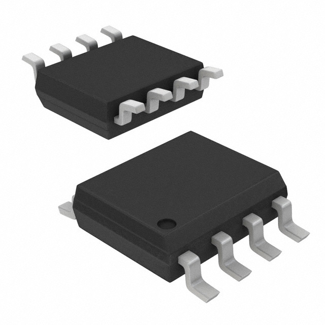
■ Packages available: 8-pin DIP, 8-pin SO, and 8-pin TSSOP
■ Available in three temperature ranges
- Commercial: 0° to +70°C
- Extended (E): -40° to +85C
- Automotive (V): -40° to +125°C
Fairchild EEPROMs are designed and tested for applications requiring high endurance, high reliability and low power consumption.
Block Diagram
VCC
VSS
WP
SDA
H.V. GENERATION
TIMING &CONTROL
START
STOP
LOGIC
CONTROL
LOGIC
SCL
SLAVE ADDRESS
REGISTER
XDEC
E2PROM
ARRAY
WORD
ADDRESS
COUNTER
R/W
YDEC
CK
DATA REGISTER
DIN
© 2002 Fairchild Semiconductor International
FM24C16U/17U Rev. A.3
1
DOUT
www.fairchildsemi.com
FM24C16U/17U – 16K-Bit Standard 2-Wire Bus Interface Serial EEPROM
September 2002
�Dual-in-Line Package (N) and SO Package (M8)
NC
1
NC
2
8
VCC
7
NC
TSSOP Package (MT8)
NC
1
VCC
2
24C16
8
SCL
7
SDA
24C16
NC
3
6
SCL
NC
3
6
VSS
VSS
4
5
SDA
NC
4
5
NC
See Package Number N08E, M08A and MTC08
Pin Names
VSS
Ground
SDA
Serial Data I/O
SCL
Serial Clock Input
NC
No Connection
VCC
Power Supply
Dual-in-Line Package (N) and SO Package (M8)
NC
1
NC
2
TSSOP Package (MT8)
8
VCC
WP
1
7
WP
VCC
2
24C17
8
SCL
7
SDA
24C17
NC
3
6
SCL
NC
3
6
VSS
VSS
4
5
SDA
NC
4
5
NC
See Package Number N08E, M08A and MTC08
Pin Names
NC
No Connection
VSS
Ground
SDA
Serial Data I/O
SCL
Serial Clock input
WP
Write Protect
VCC
Power Supply
NOTE: Pins designated as "NC" are typically unbonded pins. However some of them are bonded for special testing purposes. Hence if a signal is applied to these pins, care
should be taken that the voltage applied on these pins does not exceed the VCC applied to the device. This will ensure proper operation.
2
FM24C16U/17U Rev. A.3
www.fairchildsemi.com
FM24C16U/17U – 16K-Bit Standard 2-Wire Bus Interface Serial EEPROM
Connection Diagrams
�FM
24
C
XX
U
F
T
LZ
E
XXX
Letter
Description
N
M8
MT8
8-pin DIP
8-pin SOIC
8-pin TSSOP
Temp. Range
None
V
E
0 to 70°C
-40 to +125°C
-40 to +85°C
Voltage Operating Range
Blank
L
LZ
4.5V to 5.5V
2.7V to 5.5V
2.7V to 5.5V and
很抱歉,暂时无法提供与“FM24C16UEM8X”相匹配的价格&库存,您可以联系我们找货
免费人工找货