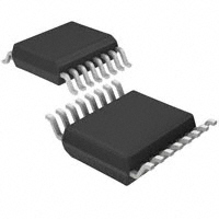
FSUSB22 — Low-Power, 2-Port, High-Speed USB 2.0 (480Mbps) Switch
March 2008
FSUSB22 — Low-Power, 2-Port, High-Speed USB 2.0 (480Mbps) Switch
Features
-40dB Off Isolation at 250MHz -40dB Non-adjacent Channel Crosstalk at 250MHz On Resistance: 4.5Ω Typical (RON) -3dB Bandwidth: 750MHz Low-Power Consumption: 1µA Maximum Control Input: TTL Compatible Bi-directional Operation USB High-Speed and Full-Speed Signaling Capability
Description
FSUSB22 is a low-power, high-bandwidth switch specially designed for applications switching high-speed USB 2.0 signals in handset and consumer applications; such as cell phone, digital camera, and notebook with hubs or controllers of limited USB I/O. The wide bandwidth (750MHz) allows signals to pass with minimum edge and phase distortion. Superior channelto-channel crosstalk results in minimal interference. It is compatible with the USB2.0 Hi-Speed standard. .
Applications
Cell Phones, PDAs, Digital Cameras, Notebook Computers
Ordering Information
Part Number
FSUSB22BQX FSUSB22QSC FSUSB22QSCX FSUSB22MTC FSUSB22MTCX
Operating Temperature Range
-40 to +85°C -40 to +85°C -40 to +85°C -40 to +85°C -40 to +85°C
Package
16-Terminal Depopulated Quad Very-Thin Flat Pack No Leads (DQFN), JEDEC MO-241, 2.5 x 3.5mm 16-Lead Quarter Size Outline Package (QSOP), JEDEC MO-137, 0.150-inch Wide 16-Lead Quarter Size Outline Package (QSOP), JEDEC MO-137, 0.150-inch Wide 16-Lead Thin Shrink Small Outline Package (TSSOP), JEDEC MO-153, 4.4mm Wide 16-Lead Thin Shrink Small Outline Package (TSSOP), JEDEC MO-153, 4.4mm Wide
Packing Method
Tape and Reel Tube Tape and Reel Tube Tape and Reel
All packages are lead free per JEDEC: J-STD-020B standard.
©2005Fairchild Semiconductor Corporation FSUSB22 • Rev. 1.0.3
www.fairchildsemi.com
�FSUSB22 — Low-Power, 2-Port, High-Speed USB 2.0 (480Mbps) Switch
Logic Diagram
D-
Analog Symbol
D+ D+ DUSB Port
USB Port
S
1
VCC
16 15 /OE 14 4B1 13 4B2 12 4A 11 3B1 10 3B2
Docking Station
1B1 2 1B2 3 1A
4
Docking Connector
2B1 5 2B2 6
USB Port
D+
D+ D-
USB 2.0 Host Controller
DD+ D-
USB Port
FSUSB22
D+ D-
2A
7 8 9
Notebook Computer
Figure 1. Logic Diagram
S 1 16 VCC /OE
GND
3A
Figure 2.
S
1
Analog Symbol
VCC
16 15 /OE
1B1 1B2 1A
2
15
1B1 2 1B2 3
3
14
4B1 4B2 4A
14 4B1
4
13
1A
4
13 4B2
2B1 2B2 2A
5
12
2B1 5 2B2 6 2A
7 8 9
12
4A
6
11
3B1 3B2 3A
11 3B1 10 3B2
7
10
GND
GND 8 9
3A
Figure 3. QSOP and TSSOP Pin Configuration
Figure 4. Pad Assignment for DQFN
Pin Descriptions
Pin #
1 2,3,5,6,10,11,13,14 8 4,7,9,12 15 16
Pin Names
S 1B1,1B2, 2B1,2B2,3B2,3B1,4B2,4B1 GND 1A,2A,3A,4A /OE VCC
Description
Select Input Bus B Ground Bus A Bus Switch Enable Supply Voltage
Truth Table
S
Don’t Care LOW HIGH
© 2005 Fairchild Semiconductor Corporation FSUSB22 • Rev. 1.0.3
OE
HIGH LOW LOW
Function
Disconnect A=B1 A=B2
www.fairchildsemi.com
2
�FSUSB22 — Low-Power, 2-Port, High-Speed USB 2.0 (480Mbps) Switch
Absolute Maximum Ratings
Stresses exceeding the absolute maximum ratings may damage the device. The device may not function or be operable above the recommended operating conditions and stressing the parts to these levels is not recommended. In addition, extended exposure to stresses above the recommended operating conditions may affect device reliability. The absolute maximum ratings are stress ratings only.
Symbol
VCC VS VIN IIK IOUT ICC / IGND TSTG ESD Supply Voltage DC Switch Voltage DC Input Voltage
(1)
Parameter
Min.
-0.5 -0.5 -0.5
Max.
4.6 VCC + 0.05 4.6 -50 128 ±100
Unit
V V V mA mA mA °C kV
DC Input Diode Current, VIN
