L272 • L272A Dual Power Operational Amplifier
June 2001 Revised May 2005
L272 • L272A Dual Power Operational Amplifier
General Description
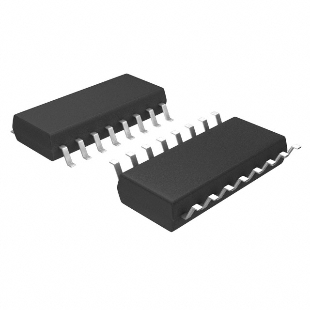
The L272 and L272A are high-power dual operational amplifier provided as a 8-DIP and 16-SOP package. The operational amplifier is designed for low impedance loads and will deliver output current up to 0.7A. The L272A offers tighter specifications for input bias current, input offset voltage and input offset currents. The L272 and L272A can be used in a wide range of applications including power supply, VCR, monitor, servo amplifier, compact disc, etc.
Features
s Output Current up to 0.7A s Operates at Low Voltage (VS(MIN) = 4V) s Low Saturation Voltage (Ip = 0.5A, VO = 1.5V) s Thermal Shutdown (TSD = 160×C) Ground Compatible Inputs s Ground Compatible Inputs s Large Common Mode & Differential Mode Range
Applications
• Servo Amplifier • Power Supply • Compact Disc • VCR • Monitor
Ordering Code:
Product Number L272M L272D2 L272D2TF L272AM L272AD2 L272AD2TF Package 8-DIP 16-SOP 16-SOP 8-DIP 16-SOP 16-SOP Packing Tube Tube Tape and Reel Tube Tube Tape and Reel Operating Temperature
�25qC to �85qC
© 2005 Fairchild Semiconductor Corporation
DS400471
www.fairchildsemi.com
�L272 • L272A
Internal Block Diagram
Pin Definitions
Pin Number 8-DIP 1 2 3 4 5 6 7 8 16-SOP 16 1 2 4/5/12/13 7 8 9 10 Pin Name OUTPUT1 VCC OUTPUT2 VEE/GND INPUT�2 INPUT�2 INPUT�1 INPUT�1 Pin Function Description Amp Output 1 Positive Supply Voltage Amp Output 2 Negative Supply Voltage (GND) Amp Negative Input 2 Amp Positive Input 2 Amp Positive Input 1 Amp Negative Input 1
www.fairchildsemi.com
2
�L272 • L272A
Absolute Maximum Ratings(Note 1)
Parameter Supply Voltage Input Voltage Differential Input Voltage DC Output Current Peak Output Current (Non Repetitive) Power Dissipation At: Tamb 50qC Operating Temperature Range Storage and Junction Temperature Symbol VCC VI VI(DIFF) IO IP Ptot Top Tstg, Tj Value 40 VS
❏rVS
Units V V V A A W
0.7 1 1
�25 to 85 �40 to 150
qC qC
Thermal Data
Parameter Thermal Resistance Junction-Ambient Maximum 8-DIP 16-SOP RTja 100 190 Symbol Value Unit
qC/W
Note 1: The “Absolute Maximum Ratings” are those values beyond which the safety of the device cannot be guaranteed. The device should not be operated at these limits. The parametric values defined in the Electrical Characteristics tables are not guaranteed at the absolute maximum ratings.
Electrical Characteristics (L272)
(VCC
�12V, VEE
�12V, TA
25qC unless otherwise specified)
Symbol VS IS VO VCC VCC VCC/2 24V, VEE 12V, VEE 0V 0V 8.0 7.5 0.3 15.0 50.0 VIN 1VPP, Unit Gain 500 VO(pp) B B 1.0 350 12.0 11.0 2.5 60.0 250 mA mA Conditions Min 4.0 Typ Max 28.0 Units V
Parameter Supply Voltage (VCC - VEE) Supply Current
Input Bias Current Input Offset Voltage Input Offset Current Slew Rate Gain-Bandwidth Product Input Resistance Large Signal Input Noise Voltage Input Noise Current Common Mode Rejection Ratio Supply Voltage Rejection Ratio Output Voltage Swing
IBIAS VIO IIO SR GBW RI GV eN IN CMRR PSRR VO VCC VCC VCC IP IP
PA
mV nA V/Ps kHz k: dB
r 10V
65.0
75.0 10.0 200
20 kHz 20 kHz 60.0
PV
pA dB dB
75.0 62.0
�15V, VEE �5V, VEE
24V, VEE 0.1A 0.5A
�15V �5V
0V
54.0
21.0 21.0 10:, GV 1dB, RL 30 dB •
23.0 22.5 60.0 0.5 160
V V dB %
Channel Separation Total Harmonic Distortion Thermal Shutdown Temperature (Note 2)
CS THD TSD
f f
1 kHz; RL 1 kHz; GV
qC
Note 2: Guaranteed by design. Not 100% tested in production.
3
www.fairchildsemi.com
�L272 • L272A
Electrical Characteristics (L272A)
(VCC
�12V, VEE
�12V, TA
25qC unless otherwise specified)
Symbol VS IS VO VCC VCC V CC/2 24V, VEE 12V, VEE 0V 0V 8.0 7.5 0.1 7.0 20.0 VIN 1VPP, Unit Gain 500 VO(pp) B B 1.0 350 12.0 11.0 1.0 30.0 100 mA mA Conditions Min 4.0 Typ Max 28.0 Units V
Parameter Supply Voltage (VCC - VEE) Supply Current
Input Bias Current Input Offset Voltage Input Offset Current Slew Rate Gain-Bandwidth Product Input Resistance Large Signal Input Noise Voltage Input Noise Current Common Mode Rejection Ratio Supply Voltage Rejection Ratio Output Voltage Swing
IBIAS VIO IIO SR GBW RI GV eN IN CMRR PSRR VO VCC VCC VCC IP IP
PA
mV nA V/Ps kHz k: dB
r 10V
65.0
75.0 10.0 200
20 kHz 20 kHz 60.0
PV
pA dB dB
75.0 62.0
�15V, VEE �5V, VEE
24V, VEE 0.1A 0.5A
�15V �5V
0V
54.0
21.0 21.0 10:, GV 1dB, RL 30 dB •
23.0 22.5 60.0 0.5 160
V V dB %
Channel Separation Total Harmonic Distortion Thermal Shutdown Temperature (Note 2)
CS THD TSD
f f
1 kHz; RL 1 kHz; GV
qC
Note 3: Guaranteed by design. Not 100% tested in production.
www.fairchildsemi.com
4
�L272 • L272A
Typical Performance Characteristics
FIGURE 1. Supply Voltage vs. Supply Current with No Load
FIGURE 2. Open Loop Voltage Gain
FIGURE 3. Output voltage Swing vs. Load Current
FIGURE 4. Output Voltage Swing vs. Load Current
FIGURE 5. Channel Separation vs. Frequency
5
www.fairchildsemi.com
�L272 • L272A
Application
�Tilt Coil Current Circuit in Monitor, 8-DIP Package!
www.fairchildsemi.com
6
�L272 • L272A
Physical Dimensions inches (millimeters) unless otherwise noted
7
www.fairchildsemi.com
�L272 • L272A Dual Power Operational Amplifier
Physical Dimensions inches (millimeters) unless otherwise noted (Continued)
Fairchild does not assume any responsibility for use of any circuitry described, no circuit patent licenses are implied and Fairchild reserves the right at any time without notice to change said circuitry and specifications. LIFE SUPPORT POLICY FAIRCHILD’S PRODUCTS ARE NOT AUTHORIZED FOR USE AS CRITICAL COMPONENTS IN LIFE SUPPORT DEVICES OR SYSTEMS WITHOUT THE EXPRESS WRITTEN APPROVAL OF THE PRESIDENT OF FAIRCHILD SEMICONDUCTOR CORPORATION. As used herein: 1. Life support devices or systems are devices or systems which, (a) are intended for surgical implant into the body, or (b) support or sustain life, and (c) whose failure to perform when properly used in accordance with instructions for use provided in the labeling, can be reasonably expected to result in a significant injury to the user. www.fairchildsemi.com 8 2. A critical component in any component of a life support device or system whose failure to perform can be reasonably expected to cause the failure of the life support device or system, or to affect its safety or effectiveness. www.fairchildsemi.com
�
很抱歉,暂时无法提供与“L272D2”相匹配的价格&库存,您可以联系我们找货
免费人工找货