MM74HCT14
Hex Inverting Schmitt Trigger
Features
Description
The MM74HCT14 utilizes advanced silicon-gate CMOS
technology to achieve the low power dissipation and
high noise immunity of standard CMOS, as well as the
capability to drive 10 LS-TTL loads.
Typical Propagation Delay: 13ns
Wide Power Supply Range: 4.5V–5.5V
Low Quiescent Current: 10µA Maximum
Low Input Current: 1µA Maximum
Fanout of 10 LS-TTL Loads
Typical Hysteresis Voltage: 0.6V at VCC = 4.5V
The 74HCT logic family is functionally and pinoutcompatible with the standard 74LS logic family. Inputs
are protected from damage due to static discharge by
internal diode clamps to VCC and ground.
MM74HCT14 — Hex Inverting Schmitt Trigger
October 2009
TTL, LS Pin-out and Input Threshold Compatible
Ordering Information
Operating
Temperature
Range
Eco
Status
MM74HCT14M
-40°C to +85°C
RoHS
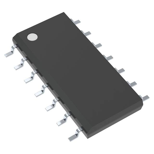
14-Lead, Small-Outline Integrated Circuit
(SOIC), JEDEC MS-012, 0.150in Narrow
Tube
MM74HCT14MX
-40°C to +85°C
RoHS
14-Lead, Small-Outline Integrated Circuit
(SOIC), JEDEC MS-012, 0.150in Narrow
Tape & Reel
MM74HCT14SJ
-40°C to +85°C
RoHS
14-Lead, Small-Outline Package (SOP),
EIAJ Type II, 5.3mm Wide
Tube
MM74HCT14SJX
-40°C to +85°C
RoHS
14-Lead, Small-Outline Package (SOP),
EIAJ Type II, 5.3mm Wide
Tape & Reel
MM74HCT14MTC
-40°C to +85°C
RoHS
14-Lead, Thin-Shrink Small-Outline Package
(TSSOP), JEDEC MO-153, 4.4mm Wide
Tube
MM74HCT14MTCX
-40°C to +85°C
RoHS
14-Lead, Thin-Shrink Small-Outline Package
(TSSOP), JEDEC MO-153, 4.4mm Wide
Tape & Reel
MM74HCT14SN
-40°C to +85°C
RoHS
14-Lead, Plastic Dual-Inline Package (PDIP),
JEDEC MS-001, 0.300in Wide
Tube
Part Number
Packing
Method
Package
For Fairchild’s definition of Eco Status, please visit: http://www.fairchildsemi.com/company/green/rohs_green.html.
© 1983 Fairchild Semiconductor Corporation
MM74HCT14 • Rev. 1.4.2
www.fairchildsemi.com
�Figure 1. Pin Assignments
MM74HCT14 — Hex Inverting Schmitt Trigger
Connection Diagram
Schematic Diagram
Figure 2. Schematic
© 1983 Fairchild Semiconductor Corporation
MM74HCT14 • Rev. 1.4.2
www.fairchildsemi.com
2
�Stresses exceeding the absolute maximum ratings may damage the device. The device may not function or be
operable above the recommended operating conditions and stressing the parts to these levels is not recommended.
In addition, extended exposure to stresses above the recommended operating conditions may affect device
reliability. The absolute maximum ratings are stress ratings only. Unless otherwise specified, all voltages are
referenced to ground.
Symbol
Parameter
Min.
Max.
Unit
VCC
Supply Voltage
–0.5
+7.0
V
VIN
DC Input Voltage
–1.5
VCC +1.5
V
DC Output Voltage
–0.5
VCC +0.5
V
VOUT
IK, IOK
Clamp Diode Current
±20
mA
IOUT
DC Output Current, Per Pin
±25
mA
ICC
DC VCC or GND Current, Per Pin
±50
mA
TSTG
TL
Storage Temperature Range
–65
Lead Temperature (Soldering 10 Seconds)
+150
°C
+260
°C
MM74HCT14 — Hex Inverting Schmitt Trigger
Absolute Maximum Ratings
Recommended Operating Conditions
The Recommended Operating Conditions table defines the conditions for actual device operation. Recommended
operating conditions are specified to ensure optimal performance to the datasheet specifications. Fairchild does not
recommend exceeding them or designing to Absolute Maximum Ratings.
Symbol
VCC
VIN, VOUT
TA
Parameter
Supply Voltage
DC Input or Output Voltage
Operating Temperature Range
© 1983 Fairchild Semiconductor Corporation
MM74HCT14 • Rev. 1.4.2
Min.
Max.
Unit
4.5
5.5
V
0
VCC
V
–40
+85
°C
www.fairchildsemi.com
3
�Symbol
Parameter
Conditions
VCC
TA=+25°C
Typ.
1.5
1.2
1.2
5.5
1.7
1.4
1.4
4.5
1.5
1.9
1.9
5.5
1.7
2.1
2.1
4.5
0.9
0.5
0.5
5.5
1.0
0.6
0.6
4.5
0.9
1.2
1.2
5.5
1.0
1.4
1.4
4.5
0.6
0.4
0.4
5.5
0.7
0.4
0.4
4.5
0.6
1.4
1.4
5.5
0.7
1.5
1.5
VIN =VIL, | IOUT | = 20µA
4.5
VCC
VIN =VIL, | IOUT | = 4.0mA
4.5
4.20
3.98
3.84
VIN =VIL, | IOUT | = 4.8mA
5.5
5.20
4.98
4.98
VIN =VIL, | IOUT | = 20µA
4.5
0
0.1
0.1
VIN =VIL, | IOUT | = 4.0mA
4.5
0.2
0.26
0.33
VIN =VIL, | IOUT | = 4.8mA
5.5
0.2
0.26
0.33
±0.1
±1.0
µA
1.0
10.0
µA
2.4
2.4
mA
Positive-Going
Threshold Voltage
Maximum
Minimum
VT-
Negative-Going
Threshold Voltage
Maximum
Minimum
VH
Hysteresis Voltage
Maximum
VOH
VOL
Minimum HIGH Level
Output Voltage
Maximum LOW Level
Voltage
IIN
Maximum Input Current VIN = VCC or GND, VIH or VIL
ICC
Maximum Quiescent
Supply Current
© 1983 Fairchild Semiconductor Corporation
MM74HCT14 • Rev. 1.4.2
Guaranteed Limits
4.5
Minimum
VT+
TA=-40°C
to +85°C Units
VIN = VCC or GND, IOUT = 0µA
VIN = 2.4V or 0.5V
5.5
5.5
V
V
V
MM74HCT14 — Hex Inverting Schmitt Trigger
DC Electrical Characteristics
VCC – 0.1 VCC – 0.1
V
V
www.fairchildsemi.com
4
�VCC = 5V, TA = 25°C, CL = 15pF, tr = tf = 6ns.
Symbol
tPHL, tPLH
Parameter
Typ.
Guaranteed Limit
Unit
10
18
ns
Maximum Propagation Delay
AC Electrical Characteristics
Unless otherwise specified, VCC = 5V±10%, CL = 50pF, tr = tf = 6ns.
Symbol
Parameter
Conditions
TA=+25°C
Typ.
tPHL, tPLH
Maximum Propagation Delay
tTLH, tTHL
Maximum Output Rise and Fall Time
CPD
Power Dissipation Capacitance
CIN
Maximum Input Capacitance
(1)
9
Per Gate
TA=-40°C
to +85°C
20
25
ns
15
19
ns
25
5
Units
Guaranteed Limits
10
pF
10
pF
Note:
1. CPD determines the no-load dynamic power consumption, PD = CPD VCC2 f+ICC VCC, and the no-load dynamic
current consumption, IS = CPD VCC f+ICC.
© 1983 Fairchild Semiconductor Corporation
MM74HCT14 • Rev. 1.4.2
MM74HCT14 — Hex Inverting Schmitt Trigger
AC Electrical Characteristics
www.fairchildsemi.com
5
�Figure 3. Low Power Oscillator
Figure 4. Oscillator Input and Output Waveforms
The following equations assume t1+t2>>tpd0+tpd1:
t 2 ≈ RCIn
f≈
VCC − VT −
VCC − VT +
1
VT + (VCC − VT − )
RCIn
VT − (VCC − VT + )
© 1983 Fairchild Semiconductor Corporation
MM74HCT14 • Rev. 1.4.2
(1)
MM74HCT14 — Hex Inverting Schmitt Trigger
Typical Applications
(2)
www.fairchildsemi.com
6
�8.75
8.50
0.65
A
7.62
14
8
B
5.60
4.00
3.80
6.00
PIN ONE
INDICATOR
1
1.70
7
0.51
0.35
1.27
0.25
1.27
LAND PATTERN RECOMMENDATION
M
C B A
(0.33)
1.75 MAX
1.50
1.25
MM74HCT14 — Hex Inverting Schmitt Trigger
Physical Dimensions
SEE DETAIL A
0.25
0.10
C
0.25
0.19
0.10 C
NOTES: UNLESS OTHERWISE SPECIFIED
A) THIS PACKAGE CONFORMS TO JEDEC
MS-012, VARIATION AB, ISSUE C,
B) ALL DIMENSIONS ARE IN MILLIMETERS.
C) DIMENSIONS DO NOT INCLUDE MOLD
GAGE PLANE
FLASH OR BURRS.
D) LANDPATTERN STANDARD:
SOIC127P600X145-14M
0.36
E) DRAWING CONFORMS TO ASME Y14.5M-1994
F) DRAWING FILE NAME: M14AREV13
0.50
0.25 X 45°
R0.10
R0.10
8°
0°
0.90
0.50
(1.04)
SEATING PLANE
DETAIL A
SCALE: 20:1
Figure 5. 14-Lead, Small-Outline Integrated Circuit (SOIC), JEDEC MS-012, 0.150in Narrow
Package drawings are provided as a service to customers considering Fairchild components. Drawings may change in any manner
without notice. Please note the revision and/or date on the drawing and contact a Fairchild Semiconductor representative to verify
or obtain the most recent revision. Package specifications do not expand the terms of Fairchild’s worldwide terms and conditions, specifically
the warranty therein, which covers Fairchild products.
Always visit Fairchild Semiconductor’s online packaging area for the most recent package drawings:
http://www.fairchildsemi.com/packaging/.
© 1983 Fairchild Semiconductor Corporation
MM74HCT14 • Rev. 1.4.2
www.fairchildsemi.com
7
�MM74HCT14 — Hex Inverting Schmitt Trigger
Physical Dimensions
Figure 6. 14-Lead, Small-Outline Package (SOP), EIAJ Type II, 5.3mm Wide
Package drawings are provided as a service to customers considering Fairchild components. Drawings may change in any manner
without notice. Please note the revision and/or date on the drawing and contact a Fairchild Semiconductor representative to verify
or obtain the most recent revision. Package specifications do not expand the terms of Fairchild’s worldwide terms and conditions, specifically
the warranty therein, which covers Fairchild products.
Always visit Fairchild Semiconductor’s online packaging area for the most recent package drawings:
http://www.fairchildsemi.com/packaging/.
© 1983 Fairchild Semiconductor Corporation
MM74HCT14 • Rev. 1.4.2
www.fairchildsemi.com
8
�MM74HCT14 — Hex Inverting Schmitt Trigger
Physical Dimensions
0.65
0.43 TYP
1.65
6.10
0.45
12.00°TOP
& BOTTOM
R0.09 min
A. CONFORMS TO JEDEC REGISTRATION MO-153,
VARIATION AB, REF NOTE 6
B. DIMENSIONS ARE IN MILLIMETERS
C. DIMENSIONS ARE EXCLUSIVE OF BURRS, MOLD FLASH,
AND TIE BAR EXTRUSIONS
D. DIMENSIONING AND TOLERANCES PER ANSI
Y14.5M, 1982
E. LANDPATTERN STANDARD: SOP65P640X110-14M
F. DRAWING FILE NAME: MTC14REV6
1.00
R0.09min
Figure 7. 14-Lead, Thin-Shrink Small-Outline Package (TSSOP), JEDEC MO-153, 4.4mm Wide
Package drawings are provided as a service to customers considering Fairchild components. Drawings may change in any manner
without notice. Please note the revision and/or date on the drawing and contact a Fairchild Semiconductor representative to verify
or obtain the most recent revision. Package specifications do not expand the terms of Fairchild’s worldwide terms and conditions, specifically
the warranty therein, which covers Fairchild products.
Always visit Fairchild Semiconductor’s online packaging area for the most recent package drawings:
http://www.fairchildsemi.com/packaging/.
© 1983 Fairchild Semiconductor Corporation
MM74HCT14 • Rev. 1.4.2
www.fairchildsemi.com
9
�MM74HCT14 — Hex Inverting Schmitt Trigger
Physical Dimensions
19.56
18.80
14
8
6.60
6.09
1
7
(1.74)
8.12
7.62
1.77
1.14
3.56
3.30
0.35
0.20
5.33 MAX
0.38 MIN
3.81
3.17
0.58
0.35
8.82
2.54
NOTES: UNLESS OTHERWISE SPECIFIED
THIS PACKAGE CONFORMS TO
A) JEDEC MS-001 VARIATION BA
B) ALL DIMENSIONS ARE IN MILLIMETERS.
DIMENSIONS ARE EXCLUSIVE OF BURRS,
C) MOLD FLASH, AND TIE BAR EXTRUSIONS.
D) DIMENSIONS AND TOLERANCES PER
ASME Y14.5-1994
E) DRAWING FILE NAME: MKT-N14AREV7
Figure 8. 14-Lead, Plastic Dual-Inline Package (PDIP), JEDEC MS-001, 0.300in Wide
Package drawings are provided as a service to customers considering Fairchild components. Drawings may change in any manner
without notice. Please note the revision and/or date on the drawing and contact a Fairchild Semiconductor representative to verify
or obtain the most recent revision. Package specifications do not expand the terms of Fairchild’s worldwide terms and conditions, specifically
the warranty therein, which covers Fairchild products.
Always visit Fairchild Semiconductor’s online packaging area for the most recent package drawings:
http://www.fairchildsemi.com/packaging/.
© 1983 Fairchild Semiconductor Corporation
MM74HCT14 • Rev. 1.4.2
www.fairchildsemi.com
10
�MM74HCT14 — Hex Inverting Schmitt Trigger
© 1983 Fairchild Semiconductor Corporation
MM74HCT14 • Rev. 1.4.2
www.fairchildsemi.com
11
�


 工商网监
湘ICP备2023018690号
工商网监
湘ICP备2023018690号
