NXP Semiconductors
Data Sheet: Technical Data
Document Number: MC9S08SU16
Rev. 2, 11/2016
MC9S08SU16 16 KB Flash
MC9S08SU16VFK
MC9S08SU8VFK
40 MHz S08L Based Microcontroller
MC9S08SU16 and MC9S08SU8 are low-cost, high-performance
and high integration UHV HCS08 8-bit microcontroller units
(MCU). It uses the enhanced S08L central processor unit with 3phase MOSFET pre-drivers unit which supports 3 high-side
PMOSes and 3 low-side NMOSes, amplifiers for current
measurement, OCP (over current protection) and OVP (over
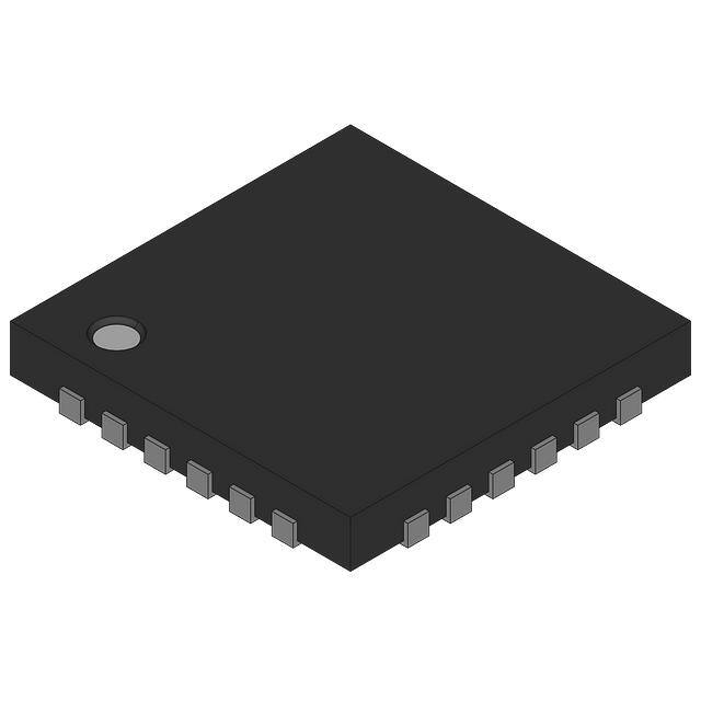
voltage protection). It is put into a 4mm x 4mm 24-pin QFN
package, targeting drone electrical speed controller, low power
motor control, small form cooling fan control and portable tools.
Core
• S08L core up to 40 MHz
• Bus up to 20 MHz
Memories
• 16 KB program flash memory for SU16 and 8 KB
program flash memory for SU8
• 768 byte SRAM, 256 B of which is unrestricted, the
other 512 B is restricted during Flash erasing and
programming
• 8 bytes regfile
System peripherals
• Windowed COP with multiple clock sources (watch
dog)
• Inter module connection module
• CRC
Clocks
• External clock input
• 32 kHz tunable internal RC oscillator
• 20 kHz low power clock
Operating Characteristics
24-pin QFN (FK)
4 x 4 x 0.65 Pitch 0.5 mm
Human-machine interface
• 5 V input/output for logical I/O
Communication interfaces
• One SCI module
• One I2C module supporting SMbus communications
interface
Analog Modules
• Two 12-bit ADC with up to 8 channels
• Analog comparator with up to 4 inputs and internal
6-bit DAC
• High voltage GDU
Timers
• Two 16-bit pulse width timers (PWT)
• Two programmable delay block (PDB)
• One 16-bit FTM
• One 16-bit modulo timer (MTIM)
• One 16-bit 6-channel PWM
Security and integrity modules
• 64-bit unique identification number per chip
• Voltage range: 4.5 to 18 V
• Temperature range (ambient): -40 to 105°C
NXP reserves the right to change the production detail specifications as may be
required to permit improvements in the design of its products.
�Ordering information
Part Number
Memory
Maximum number of I\O's
Flash (KB)
SRAM (Byte)
MC9S08SU16VFK
16
768
17
MC9S08SU8VFK
8
768
17
Related resources
Type
Description
Resource
Selector
Guide
The NXP Solution Advisor is a web-based tool that features
interactive application wizards and a dynamic product selector.
Solution Advisor
Reference
Manual
The Reference Manual contains a comprehensive description of the
structure and function (operation) of a device. 1
MC9S08SU16RM
Data Sheet
The Data Sheet includes electrical characteristics and signal
connections.
MC9S08SU161
Chip Errata
The chip mask set Errata provides additional or corrective information xN88M2
for a particular device mask set.
Package
drawing
Package dimensions are provided in package drawings.
QFN 24-pin: 98ASA00602D
1. To find the associated resource, go to nxp.com and perform a search using this term.
2. To find the associated resource, go to nxp.com and perform a search using this term with the “x” replaced by the
revision of the device you are using.
Figure 1 shows the functional modules in the chip.
2
NXP Semiconductors
MC9S08SU16 16 KB Flash, Rev. 2, 11/2016
�BKGD
CPU
Memory
Map
Controller
Background
Debg
Controller
Interrupt
Unit
Clock Generation
Internal Clock Source(ICS)
Internal
32 kHz
FLL
Flash
Line Buffer
S08L Core
S08L Bus
User Flash
16 KB (SU16)
8 KB (SU8)
User RAM
768 Bytes
Peripheral
Bus Bridge
Interrupt Priority
Controller
Cyclic Redundancy
Check (CRC)
Windowed
Watchdog (WCOP)
Power Management
Controller (PMC)
Modulo Timer
(MTIM)
System Integration
Module (SIM)
Low Power Osc (LPO)
Internal
20 kHz LPO
Peripheral Bus
Analog Signals
SCI
I2C
IRQ
FTM
Ch0,1
PWT
0,1
PDB
Ch0,1
Inter-Module
Crossbar
CMP
ADC0 ADC1
+ 6-bit DAC 12-bit 12-bit
PWM
Gate Pre-Driver Unit (GDU)
Predriver + 5 CMP + 2 OPAMP
Inter Module Crossbar Inputs
Inter Module Crossbar Outputs
Pre
Driver
GPIO Port A&B&C and Peripheral MUX
Analog Inpus
Package Pins
Package Pins
Motor Drive
Figure 1. Functional block diagram
MC9S08SU16 16 KB Flash, Rev. 2, 11/2016
3
NXP Semiconductors
�Table of Contents
1 Ratings.................................................................................... 5
1.1 Thermal handling ratings............................................... 5
1.2 Moisture handling ratings.............................................. 5
1.3 ESD handling ratings.....................................................5
1.4 Voltage and current operating ratings........................... 6
2 General................................................................................... 7
2.1 Nonswitching electrical specifications........................... 7
2.1.1 DC characteristics............................................. 7
2.1.2 Supply current characteristics........................... 12
2.1.3 EMC performance............................................. 14
2.2 Switching specifications.................................................15
2.2.1 Control timing.................................................... 15
2.2.2 FTM module timing............................................16
Thermal specifications...................................................17
2.3.1 Thermal operating requirements....................... 17
2.3.2 Thermal characteristics..................................... 18
3 Peripheral operating requirements and behaviors.................. 18
3.1 ICS characteristics.........................................................18
3.2 NVM specifications........................................................ 19
3.3 Analog........................................................................... 20
3.3.1 ADC characteristics...........................................20
3.3.2 CMP and 6-bit DAC electrical specifications..... 23
3.3.3 GDU characteristics.......................................... 26
3.4 Communication interfaces............................................. 29
2.3
4
NXP Semiconductors
3.4.1 Inter-Integrated Circuit Interface (I2C) timing.... 29
4 Dimensions............................................................................. 30
4.1 Obtaining package dimensions..................................... 30
5 Pinout...................................................................................... 30
5.1 Signal multiplexing and pin assignments.......................30
5.2 Pinout ........................................................................... 32
6 Part identification.....................................................................32
6.1 Description.....................................................................32
6.2 Format........................................................................... 33
6.3 Fields............................................................................. 33
6.4 Example.........................................................................33
7 Terminology and guidelines.................................................... 33
7.1 Definition: Operating requirement..................................33
7.2 Definition: Operating behavior....................................... 34
7.3 Definition: Attribute........................................................ 34
7.4 Definition: Rating........................................................... 35
7.5 Result of exceeding a rating.......................................... 35
7.6 Relationship between ratings and operating
requirements..................................................................36
7.7 Guidelines for ratings and operating requirements........36
7.8 Definition: Typical value.................................................36
7.9 Typical value conditions................................................ 37
7.10 Parameter Classification................................................38
8 Revision history.......................................................................38
MC9S08SU16 16 KB Flash, Rev. 2, 11/2016
�Ratings
1 Ratings
1.1 Thermal handling ratings
Symbol
Description
Min.
Max.
Unit
Notes
TSTG
Storage temperature
–55
150
°C
1
TSDR
Solder temperature, lead-free
—
260
°C
2
1. Determined according to JEDEC Standard JESD22-A103, High Temperature Storage Life.
2. Determined according to IPC/JEDEC Standard J-STD-020, Moisture/Reflow Sensitivity Classification for Nonhermetic
Solid State Surface Mount Devices.
1.2 Moisture handling ratings
Symbol
MSL
Description
Moisture sensitivity level
Min.
Max.
Unit
Notes
—
3
—
1
1. Determined according to IPC/JEDEC Standard J-STD-020, Moisture/Reflow Sensitivity Classification for Nonhermetic
Solid State Surface Mount Devices.
1.3 ESD handling ratings
Symbol
Description
Min.
Max.
Unit
Notes
VHBM
Electrostatic discharge voltage, human body model
-2000
+2000
V
1
VCDM
Electrostatic discharge voltage, charged-device
model
-500
+500
V
2
Latch-up current at ambient temperature of 105°C
-100
+100
mA
ILAT
1. Determined according to JEDEC Standard JESD22-A114, Electrostatic Discharge (ESD) Sensitivity Testing Human
Body Model (HBM).
2. Determined according to JEDEC Standard JESD22-C101, Field-Induced Charged-Device Model Test Method for
Electrostatic-Discharge-Withstand Thresholds of Microelectronic Components.
MC9S08SU16 16 KB Flash, Rev. 2, 11/2016
5
NXP Semiconductors
�Ratings
1.4 Voltage and current operating ratings
Absolute maximum ratings are stress ratings only, and functional operation at the
maximum is not guaranteed. Stress beyond the limits specified in below table may
affect device reliability or cause permanent damage to the device. For functional
operating conditions, refer to the remaining tables in this document.
This device contains circuitry protecting against damage due to high static voltage or
electrical fields; however, it is advised that normal precautions be taken to avoid
application of any voltages higher than maximum-rated voltages to this high-impedance
circuit. Reliability of operation is enhanced if unused inputs are tied to an appropriate
logic voltage level (for instance, either VSS or VDDX) or the programmable pullup
resistor associated with the pin is enabled.
Symbol
Description
VDD
Supply voltage
drivers1
Min.
Max.
Unit
4.5
18
V
4.20
5.25
V
—
50
mA
VDDX
Supply voltage to digital I/O
IDDX
Maximum current into VDDX
VDIO
Digital input voltage (except RESET or true open drain pin
PTA4 and PTA5)
-0.3
VDDX+0.3
V
Digital input voltage (true open drain pin PTA4 and PTA5)
-0.3
VDDX+0.3
V
Analog2, RESET input voltage
-0.3
VDDX+0.3
V
Instantaneous maximum current single pin limit (applies to
all port pins)
-25
25
mA
VAIO
ID
1. See Table 2 for detail.
2. All digital I/O pins, except open-drain pin PTA4 and PTA5, are internally clamped to VSS and VDDX. PTA4 and PTA5 is
only clamped to VSS.
6
NXP Semiconductors
MC9S08SU16 16 KB Flash, Rev. 2, 11/2016
�General
2 General
2.1 Nonswitching electrical specifications
2.1.1 DC characteristics
This section includes information about power supply requirements and I/O pin
characteristics.
Table 1. DC characteristics
Symbol
C
—
—
VOH
P
Descriptions
Operating voltage
Output high
voltage
P
Min
Typical1
Max
Unit
—
4.5
—
18
V
All I/O pins,
standard-drive
strength
5 V, Iload =
-5 mA
VDDX - 0.8
—
—
V
High current drive
pins, high-drive
strength2
5 V, Iload =
-20 mA
VDDX - 0.8
—
—
V
IOHT
D
Output high
current
Max total IOH for all
ports
5V
—
—
-100
mA
VOL
P
Output low
voltage
All I/O pins,
standard-drive
strength
5 V, Iload =
5 mA
—
—
0.8
V
High current drive
pins, high-drive
strength2
5 V, Iload
=20 mA
—
—
0.8
V
P
IOLT
D
Output low
current
Max total IOL for all
ports
5V
—
—
100
mA
VIH
P
Input high
voltage
All digital inputs
VDDX>4.5V
0.70 × VDDX
—
—
V
VDDX>2.7V
0.75 × VDDX
—
—
Input low
voltage
All digital inputs
VDDX>4.5V
—
—
0.30 × VDDX
VDDX>2.7V
—
—
0.35 × VDDX
C
VIL
P
C
V
Vhys
C
Input
hysteresis
All digital inputs
—
0.06 × VDDX
—
—
mV
|IIn|
P
Input leakage
current
All input only pins
(per pin)
VIN = VDDX
or VSS
—
0.1
1
µA
|IOZTOT|
C
Total leakage All input only and I/O VIN = VDDX
combined for
or VSS
all inputs and
Hi-Z pins
—
—
2
µA
Table continues on the next page...
MC9S08SU16 16 KB Flash, Rev. 2, 11/2016
7
NXP Semiconductors
�Nonswitching electrical specifications
Table 1. DC characteristics (continued)
Min
Typical1
Max
Unit
—
30.0
—
50.0
kΩ
PTA4 and PTA5 pin
—
30.0
—
60.0
kΩ
Pulldown
resistors
PTB3, PTB4 and
PTB5 pin
—
30
40
50
kΩ
DC injection
current5, 6, 7
Single pin limit
VIN < VSS,
VIN > VDDX
-2
—
2
mA
-5
—
25
Symbol
C
Descriptions
RPU
P
Pullup
resistors
All digital inputs,
when enabled (all
I/O pins other than
PTA4 and PTA5)
RPU3
P
Pullup
resistors
RPD4
P
IIC
D
Total MCU limit,
includes sum of all
stressed pins
CIn
C
Input capacitance, all pins
—
—
—
7
pF
VRAM
C
RAM retention voltage
—
2.0
—
—
V
1. Typical values are measured at 25 °C. Characterized, not tested.
2. Only PTB3, PTB4, PTB5, and PTB7 are high drive pins, and support ultra-high current output.
3. The specified resistor value is the actual value internal to the device. The pullup value may appear higher when
measured externally on the pin.
4. The specified resistor value is the actual value internal to the device. The pulldown value may appear higher when
measured externally on the pin.
5. All functional non-supply pins, except PTA4 and PTA5, are internally clamped to VSS and VDDX.
6. Input must be current-limited to the value specified. To determine the value of the required current-limiting resistor,
calculate resistance values for positive and negative clamp voltages, then use the large one.
7. Power supply must maintain regulation within operating VDD range during instantaneous and operating maximum current
conditions. If the positive injection current (VIn > VDD) is higher than IDD, the injection current may flow out of VDD and
could result in external power supply going out of regulation. Ensure that external VDD load will shunt current higher than
maximum injection current when the MCU is not consuming power, such as no system clock is present, or clock rate is
very low (which would reduce overall power consumption).
Table 2. Power supply electrical characteristics
Symbol
VDDX
Description
Output voltage VDDX
Min.
Typical
Max.
Unit
Run mode 4.5 V≤ VDD 4 MHz
fADCK < 4 MHz
Symb
Min
Typ1
Max
RAS
—
—
2
—
—
5
—
—
5
—
—
10
—
—
10
0.4
—
8.0
0.4
—
4.0
8-bit mode
Unit
Comment
kΩ
External to
MCU
MHz
—
(all valid fADCK)
ADC
conversion
clock
frequency
High speed (ADLPC=0)
fADCK
Low power (ADLPC=1)
1. Typical values assume VDDA = 5.0 V, Temp = 25°C, fADCK=1.0 MHz unless otherwise stated. Typical values are for
reference only and are not tested in production.
SIMPLIFIED
INPUT PIN EQUIVALENT
CIRCUIT
Pad
leakage
due to
input
protection
ZAS
R AS
z ADIN
SIMPLIFIED
CHANNEL SELECT
CIRCUIT
ADC SAR
ENGINE
R ADIN
v ADIN
v AS
C AS
R ADIN
INPUT PIN
R ADIN
INPUT PIN
R ADIN
INPUT PIN
C ADIN
Figure 11. ADC input impedance equivalency diagram
Table 12. 12-bit ADC Characteristics (VREFH = VDDA, VREFL = VSSA)
Characteristic
Conditions
Supply current
C
Symb
Min
Typ1
Max
Unit
T
IDDA
—
133
—
µA
ADLPC = 1
ADLSMP = 1
Table continues on the next page...
MC9S08SU16 16 KB Flash, Rev. 2, 11/2016
21
NXP Semiconductors
�Peripheral operating requirements and behaviors
Table 12. 12-bit ADC Characteristics (VREFH = VDDA, VREFL = VSSA) (continued)
Characteristic
Conditions
C
Symb
Min
Typ1
Max
Unit
T
IDDA
—
218
—
µA
T
IDDA
—
327
—
µA
T
IDDAD
—
582
990
µA
ADCO = 1
Supply current
ADLPC = 1
ADLSMP = 0
ADCO = 1
Supply current
ADLPC = 0
ADLSMP = 1
ADCO = 1
Supply current
ADLPC = 0
ADLSMP = 0
ADCO = 1
Supply current
Stop, reset, module
off
T
IDDA
—
0.011
1
µA
ADC asynchronous
clock source
High speed (ADLPC
= 0)
T
fADACK
2
3.3
5
MHz
1.25
2
3.3
—
20
—
—
40
—
—
3.5
—
—
23.5
—
—
±5.5
—
Low power (ADLPC
= 1)
Conversion time
(including sample
time)
Short sample
(ADLSMP = 0)
Sample time
Short sample
(ADLSMP = 0)
T
tADC
Long sample
(ADLSMP = 1)
T
tADS
Long sample
(ADLSMP = 1)
Total unadjusted
Error2, 3
Differential NonLinearity3
12-bit mode
T
10-bit mode
T
—
±1.7
±2.0
8-bit mode
T
—
±0.9
±1.0
12-bit mode
T
—
1.4
—
10-bit mode5
P
—
0.5
—
—
0.15
—
—
1.4
—
Zero-scale
Full-scale
error6
error7
DNL
mode5
T
12-bit mode
T
10-bit mode
T
—
0.5
—
8-bit mode
T
—
0.15
—
12-bit mode
C
—
±2.0
—
10-bit mode
T
—
±0.25
±1.0
8-bit mode
T
—
±0.65
±1.0
12-bit mode
T
—
±2.5
—
8-bit
Integral NonLinearity3
ETUE
INL
EZS
EFS
ADCK
cycles
ADCK
cycles
LSB4
LSB4
LSB4
LSB4
LSB4
Table continues on the next page...
22
NXP Semiconductors
MC9S08SU16 16 KB Flash, Rev. 2, 11/2016
�Peripheral operating requirements and behaviors
Table 12. 12-bit ADC Characteristics (VREFH = VDDA, VREFL = VSSA) (continued)
Min
Typ1
Max
T
—
±0.5
±1.0
8-bit mode
T
—
±0.5
±1.0
≤12 bit modes
D
EQ
—
—
±0.5
LSB4
Input leakage error8 all modes
D
EIL
Temp sensor slope
D
m
mV/°C
Characteristic
Quantization error
Conditions
C
10-bit mode
-40°C– 25°C
Symb
25°C– 125°C
Temp sensor
voltage
25°C
D
VTEMP25
IIn * RAS
Unit
mV
—
3.266
—
—
3.638
—
—
1.36
—
V
1. Typical values assume VDDX = 5.0 V, VDD ≥ 5.3 V, Temp = 25°C, fADCK=1.0 MHz unless otherwise stated. Typical
values are for reference only and are not tested in production.
2. Includes quantization.
3. To get better ADC performance: For the application case of VDD


 工商网监
湘ICP备2023018690号
工商网监
湘ICP备2023018690号
