IXD_609SI
Automotive Grade
9-Ampere, Low-Side, Ultrafast MOSFET Drivers
INTEGRATED CIRCUITS DIVISION
Features
•
•
•
•
•
•
•
•
•
Description
AEC Q100 Qualified
9A Peak Source/Sink Drive Current
Wide Operating Voltage Range: 4.5V to 35V
AEC Q100 Grade 1 -40°C to +125°C Operating
Temperature Range
Logic Input Withstands Negative Swing of up to 5V
Matched Rise and Fall Times
Low Propagation Delay Time
Low, 10A Supply Current
Low Output Impedance
Applications
•
•
•
•
Automotive DC/DC Regulators
Electronic Power Steering
Electric Vehicle Power Train Drives
Brushless DC Motors
The IXD_609SI is an automotive grade, high-speed
gate driver that is qualified according to AEC Q100
standards. The IXD_609SI output can source and sink
9A of peak current, while producing rise and fall times
of less than 45ns. Both the output and input are rated
to 35V. The input is virtually immune to latch-up, and
proprietary circuitry eliminates cross conduction and
"shoot-through." The IXD_609SI has a Grade 1, -40°C
to +125°C ambient operating temperature range.
The IXDD609SI is configured as a non-inverting driver
with an enable, the IXDN609SI is configured as a
non-inverting driver, and the IXDI609SI is configured
as an inverting driver. The AEC Q100 qualified
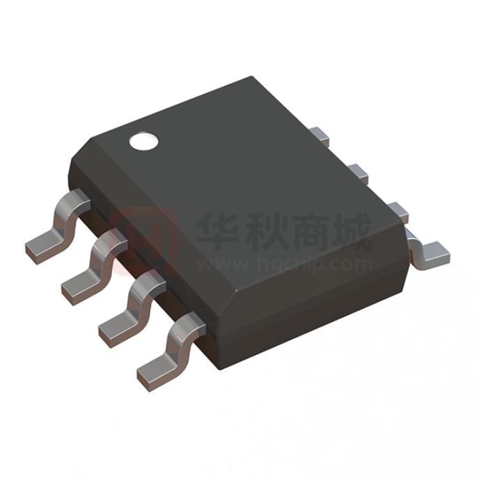
IXD_609SI is available in an 8-pin Power SOIC
package with an exposed metal back.
Ordering Information
Logic
Configuration
Part Number
Package Type
IXDD609SI
IN
IXDD609SITR
IXDI609SI
IXDI609SITR
OUT
8-Pin Power SOIC
with Exposed Metal Back
IXDN609SI
IXDN609SITR
DS-IXD_609SI-R02
IN
Quantity
Tube
100
Tape & Reel
2000
Tube
100
Tape & Reel
2000
Tube
100
Tape & Reel
2000
OUT
EN
IN
Packing
Method
OUT
www.ixysic.com
1
�INTEGRATED CIRCUITS DIVISION
IXD_609SI
1. Specifications . . . . . . . . . . . . . . . . . . . . . . . . . . . . . . . . . . . . . . . . . . . . . . . . . . . . . . . . . . . . . . . . . . . . . . . . . . . . . . . . . . . . . . . . . . . . . .
1.1 Pin Configurations . . . . . . . . . . . . . . . . . . . . . . . . . . . . . . . . . . . . . . . . . . . . . . . . . . . . . . . . . . . . . . . . . . . . . . . . . . . . . . . . . . . . . . .
1.2 Pin Definitions . . . . . . . . . . . . . . . . . . . . . . . . . . . . . . . . . . . . . . . . . . . . . . . . . . . . . . . . . . . . . . . . . . . . . . . . . . . . . . . . . . . . . . . . . .
1.3 Absolute Maximum Ratings . . . . . . . . . . . . . . . . . . . . . . . . . . . . . . . . . . . . . . . . . . . . . . . . . . . . . . . . . . . . . . . . . . . . . . . . . . . . . . . .
1.4 Recommended Operating Conditions . . . . . . . . . . . . . . . . . . . . . . . . . . . . . . . . . . . . . . . . . . . . . . . . . . . . . . . . . . . . . . . . . . . . . . . .
1.5 Electrical Characteristics: TA = 25°C . . . . . . . . . . . . . . . . . . . . . . . . . . . . . . . . . . . . . . . . . . . . . . . . . . . . . . . . . . . . . . . . . . . . . . . . .
1.6 Electrical Characteristics: TA = - 40°C to +125°C . . . . . . . . . . . . . . . . . . . . . . . . . . . . . . . . . . . . . . . . . . . . . . . . . . . . . . . . . . . . . . .
1.7 Thermal Characteristics . . . . . . . . . . . . . . . . . . . . . . . . . . . . . . . . . . . . . . . . . . . . . . . . . . . . . . . . . . . . . . . . . . . . . . . . . . . . . . . . . . .
3
3
3
3
3
4
4
5
2. IXD_609SI Performance . . . . . . . . . . . . . . . . . . . . . . . . . . . . . . . . . . . . . . . . . . . . . . . . . . . . . . . . . . . . . . . . . . . . . . . . . . . . . . . . . . . . . . 5
2.1 Timing Diagrams . . . . . . . . . . . . . . . . . . . . . . . . . . . . . . . . . . . . . . . . . . . . . . . . . . . . . . . . . . . . . . . . . . . . . . . . . . . . . . . . . . . . . . . . 5
2.2 Characteristics Test Diagram. . . . . . . . . . . . . . . . . . . . . . . . . . . . . . . . . . . . . . . . . . . . . . . . . . . . . . . . . . . . . . . . . . . . . . . . . . . . . . . 5
3. Block Diagrams & Truth Tables . . . . . . . . . . . . . . . . . . . . . . . . . . . . . . . . . . . . . . . . . . . . . . . . . . . . . . . . . . . . . . . . . . . . . . . . . . . . . . . .
3.1 IXDD609SI. . . . . . . . . . . . . . . . . . . . . . . . . . . . . . . . . . . . . . . . . . . . . . . . . . . . . . . . . . . . . . . . . . . . . . . . . . . . . . . . . . . . . . . . . . . . .
3.2 IXDI609SI. . . . . . . . . . . . . . . . . . . . . . . . . . . . . . . . . . . . . . . . . . . . . . . . . . . . . . . . . . . . . . . . . . . . . . . . . . . . . . . . . . . . . . . . . . . . . .
3.3 IXDN609SI. . . . . . . . . . . . . . . . . . . . . . . . . . . . . . . . . . . . . . . . . . . . . . . . . . . . . . . . . . . . . . . . . . . . . . . . . . . . . . . . . . . . . . . . . . . . .
6
6
6
6
4. Typical Performance Characteristics . . . . . . . . . . . . . . . . . . . . . . . . . . . . . . . . . . . . . . . . . . . . . . . . . . . . . . . . . . . . . . . . . . . . . . . . . . . 7
5. Manufacturing Information . . . . . . . . . . . . . . . . . . . . . . . . . . . . . . . . . . . . . . . . . . . . . . . . . . . . . . . . . . . . . . . . . . . . . . . . . . . . . . . . . . .
5.1 Moisture Sensitivity . . . . . . . . . . . . . . . . . . . . . . . . . . . . . . . . . . . . . . . . . . . . . . . . . . . . . . . . . . . . . . . . . . . . . . . . . . . . . . . . . . . . .
5.2 ESD Sensitivity . . . . . . . . . . . . . . . . . . . . . . . . . . . . . . . . . . . . . . . . . . . . . . . . . . . . . . . . . . . . . . . . . . . . . . . . . . . . . . . . . . . . . . . .
5.3 Soldering Profile. . . . . . . . . . . . . . . . . . . . . . . . . . . . . . . . . . . . . . . . . . . . . . . . . . . . . . . . . . . . . . . . . . . . . . . . . . . . . . . . . . . . . . . .
5.4 Board Wash . . . . . . . . . . . . . . . . . . . . . . . . . . . . . . . . . . . . . . . . . . . . . . . . . . . . . . . . . . . . . . . . . . . . . . . . . . . . . . . . . . . . . . . . . . .
2
www.ixysic.com
10
10
10
10
10
R02
�IXD_609SI
INTEGRATED CIRCUITS DIVISION
1 Specifications
1.1 Pin Configurations
1.2 Pin Definitions
IXDD609SI
Pin Name
VCC
1
8
VCC
IN
2
7
OUT
EN
3
6
OUT
GND
4
5
GND
Description
IN
Logic Input
EN
Output Enable - Drive pin low to disable output,
and force output to a high impedance state
OUT
Output - Sources or sinks current to turn-on or
turn-off a discrete MOSFET or IGBT
OUT
Inverted Output - Sources or sinks current to
turn-on or turn-off a discrete MOSFET or IGBT
VCC
Supply Voltage - Provides power to the device
GND
Ground - Common ground reference for the
device
IXDI609SI
VCC
1
8
VCC
IN
2
7
OUT
NC
3
6
OUT
GND
4
5
GND
NC
Not connected
IXDN609SI
VCC
1
8
VCC
IN
2
7
OUT
NC
3
6
OUT
GND
4
5
GND
1.3 Absolute Maximum Ratings
Parameter
Supply Voltage
Input Voltage
Output Current
Junction Temperature
Storage Temperature
Symbol
Minimum
Maximum
Units
VCC
-0.3
40
V
VIN, VEN
-5
VCC+0.3
V
IOUT
TJ
TSTG
-
±9
-55
+150
A
°C
-65
+150
°C
Unless stated otherwise, absolute maximum electrical ratings are at 25°C
Absolute maximum ratings are stress ratings. Stresses in excess of these ratings can cause permanent damage to the device.
Functional operation of the device at conditions beyond those indicated in the operational sections of this data sheet is not
implied.
1.4 Recommended Operating Conditions
Parameter
Supply Voltage
Operating Temperature Range
R02
Symbol
Range
Units
VCC
TA
4.5 to 35
V
-40 to +125
°C
www.ixysic.com
3
�IXD_609SI
INTEGRATED CIRCUITS DIVISION
1.5 Electrical Characteristics: TA = 25°C
Test Conditions: 4.5V < VCC < 35V (unless otherwise noted).
Parameter
Conditions
Symbol
Minimum
Typical
Maximum
Input Voltage, High
4.5V < VCC < 18V
VIH
3.0
-
-
Input Voltage, Low
4.5V < VCC < 18V
VIL
-
-
0.8
2/3VCC
-
±10
A
-
1/3VCC
V
Input Current
0V < VIN < VCC
IIN
EN Input Voltage, High
IXDD609SI only
VENH
EN Input Voltage, Low
IXDD609SI only
VENL
Output Voltage, High
-
VOH
VCC-0.025
-
-
Output Voltage, Low
-
VOL
-
-
0.025
Output Resistance, High State
VCC=18V, IOUT=-100mA
ROH
-
0.6
1
Output Resistance, Low State
ROL
-
0.4
0.8
IDC
-
-
±2
Rise Time
VCC=18V, IOUT=100mA
Limited by package power
dissipation
VCC=18V, CLOAD=10nF
tr
-
22
35
Fall Time
VCC=18V, CLOAD=10nF
tf
-
15
25
On-Time Propagation Delay
VCC=18V, CLOAD=10nF
tondly
-
40
60
Off-Time Propagation Delay
Enable to Output-High Delay Time
(IXDD609SI Only)
Disable to High Impedance State Delay Time
(IXDD609SI Only)
Enable Pull-Up Resistor
VCC=18V, CLOAD=10nF
toffdly
-
42
60
tENOH
-
25
60
tDOLD
-
35
60
REN
-
200
1