Thyristors
Surface Mount – 100V -600V > MCR12DSM, MCR12DSN
MCR12DSM, MCR12DSN
Description
The MCR12DSM and MCR12DSN are designed for high
volume, low cost, industrial and consumer applications
such as motor control; process control; temperature, light
and speed control; CDI (Capacitive Discharge Ignition); and
small engines.
Features
• Small Size
• Passivated Die Surface for
Reliability and Uniformity
• Low Level Triggering and
Holding Characteristics
• UL Recognized compound
meeting flammability
rating V-0
• ESD Ratings: Human
Body Model, 3B > 8000V
Machine Model, C > 400V
Pin Out
4
4
Functional Diagram
G
1 2
3
A
1
2
3
K
Additional Information
Datasheet
Resources
Samples
© 2020 Littelfuse, Inc.
Specifications are subject to change without notice.
Revised: 09/09/20
�Thyristors
Surface Mount – 100V -600V > MCR12DSM, MCR12DSN
Maximum Ratings (TJ = 25°C unless otherwise noted)
Rating
Symbol
Value
Unit
VDRM
VRRM
600
800
V
On−State RMS Current (180º Conduction Angles; TC = 75ºC)
IT(RMS)
12
A
Average On-State Current (180º Conduction Angles; TC = 75ºC)
IT (AV)
7.6
A
Non-Repetitive Surge Current (1/2 Cycle, Sine Wave 60 Hz, TJ = 110°C)
ITSM
100
A
Circuit Fusing Consideration (t = 8.3 ms)
I2t
41
A2s
PGM
5.0
W
PG (AV)
0.5
W
Peak Repetitive Off−State Voltage (Note 1)
(TC = − 40 to +110°C, Sine Wave, 50 to 60 Hz, RGK = 1 k Ω)
MCR12DSM
MCR12DSN
Forward Peak Gate Power (Pulse Width ≤ 1.0 µsec, TC= 75°C)
Forward Average Gate Power (t = 8.3 ms, TC = 75ºC)
Forward Peak Gate Current (Pulse Width ≤ 1.0 µsec, TC= 75°C)
IGM
2.0
A
Operating Junction Temperature Range
TJ
-40 to +110
°C
Storage Temperature Range
Tstg
-40 to +150
°C
Stresses exceeding Maximum Ratings may damage the component. Maximum Ratings are stress ratings only. Functional operation above the Recommended Operating Conditions is not implied. Extended exposure to stresses above
the Recommended Operating Conditions may affect component reliability.
1. VDRM and VRRM for all types can be applied on a continuous basis. Ratings apply for zero or negative gate voltage; however, positive gate voltage shall not be applied concurrent with negative potential on the anode. Blocking voltages
shall not be tested with a constant current source such that the voltage ratings of the component are exceeded.
Thermal Characteristics
Rating
Symbol
Value
Thermal Resistance, Junction−to−Case
RƟJC
2.2
Thermal Resistance, Junction−to−Ambient
RƟJA
88
Thermal Resistance, Junction−to−Ambient (Note 2)
RƟJA
80
Maximum Lead Temperature for Soldering Purposes (Note 3)
TL
260
Unit
°C/W
°C
Electrical Characteristics - OFF (TJ = 25°C unless otherwise noted)
Characteristic
Peak Repetitive Forward or Reverse Blocking Current
(VAK = Rated VDRM or VRRM, RGK = 1.0 k Ω)4
Symbol
Min
IDRM
IRRM
-
-
10
-
-
500
TJ = 25°C
TJ = 110°C
Typ
Max
Unit
µA
Electrical Characteristics - ON (TJ = 25°C unless otherwise noted)
Characteristic
Symbol
Min
Typ
Peak Reverse Gate Blocking Voltage, (IGR = 10 µA)
VGRM
10
12.5
18
V
Peak Reverse Gate Blocking Current, (VGR = 10 V)
IGRM
_
_
1.2
µA
V
Peak Forward On−State Voltage (Note 5), (ITM = 20 A)
Gate Trigger Voltage (Note 6)
(VAK= 12 Vdc; RL = 100 Ω, TC =110º)
Gate Trigger Voltage (Continuous dc) (Note 6)
(VAK = 12 V; RL = 100 Ω)
VTM
TJ = 25°C
TJ = –40°C
IGT
TJ = 25°C
TJ = –40°C
VGT
TJ = 25°C
TJ = –40°C
Latching Current
(VD = 12 V, IG = 2.0 mA, RGK = 1 kΩ)
TJ = –40°C
TJ = 25°C
Peak Reverse Gate Blocking Current (VGR = 10 V)
Turn-On Time (Source Voltage = 12 V, RS = 6.0 KΩ, IT = 16 A(pk), RGK = 1.0 KΩ)
(VD = Rated VDRM, Rise Time = 20 ns, Pulse Width = 10 µs)
–
1.3
1.9
5.0
12
200
_
_
300
0.45
0.65
1.0
Unit
µA
V
_
_
1.5
0.2
–
–
0.5
1.0
6.0
_
_
10
0.5
1.0
6.0
_
_
10
IRGM
_
_
1.2
µA
tgt
_
2.0
5.0
µs
TJ = 110°C
Holding Current
(VD = 12 V, Initiating Current = 200 mA, RGK = 1 kΩ)
Max
IH
IL
mA
mA
© 2020 Littelfuse, Inc.
Specifications are subject to change without notice.
Revised: 09/09/20
�Thyristors
Surface Mount – 100V -600V > MCR12DSM, MCR12DSN
Dynamic Characteristics
Characteristic
Symbol
Min
Typ
Max
Unit
Critical Rate of Rise of Off−State Voltage
(VD = 0.67 x Rated VDRM, Exponential Waveform, RGK = 1.0 K, TJ = 110°C)
dv/dt
2.0
10
−
V/µs
Critical Rate of Rise of On−State Current
(IPK = 50 A, PW = 40 sec, diG/dt = 1 A/sec, IGT = 10 mA)
di/dt
−
50
100
A/µs
2. These ratings are applicable when surface mounted on the minimum pad sizes recommended.
3. 1/8" from case for 10 seconds.
4. Ratings apply for negative gate voltage or RGK = 1.0 kΩ Devices shall not have a positive gate voltage concurrently with a negative voltage on the anode. Component should not be tested with a constant current source for forward
and reverse blocking capability such that the voltage applied exceeds the rated blocking voltage.
5. Pulse Test: Pulse Width ≤ 2.0 msec, Duty Cycle ≤ 2%.
6. RGK current not included in measurement.
Voltage Current Characteristic of SCR
Symbol
Parameter
VDRM
Peak Repetitive Forward Off State Voltage
IDRM
Peak Forward Blocking Current
VRRM
Peak Repetitive Reverse Off State Voltage
IRRM
Peak Reverse Blocking Current
VTM
Maximum On State Voltage
IH
Holding Current
+Current
VTM
Anode+
On State
IRRM at VRRM
IH
+Voltage
Reverse Blocking Region
(Off State)
Reverse Avalanche Region
IDRM at VDRM
Forward Blocking Region
(Off State)
Anode-
Figure 1. Average Current Derating
Figure 2. On−State Power Dissipation
© 2020 Littelfuse, Inc.
Specifications are subject to change without notice.
Revised: 09/09/20
�Thyristors
Surface Mount – 100V -600V > MCR12DSM, MCR12DSN
Figure 3. On−State Characteristics
Figure 4. Transient Thermal Response
Figure 5. Typical Gate Trigger Current vs Junction Temperature
Figure 6. Typical Gate Trigger Voltage vs Junction Temperature
Figure 7. Typical Holding Current vs Junction Temperature
Figure 8. Typical Latching Current vs Junction Temperature
© 2020 Littelfuse, Inc.
Specifications are subject to change without notice.
Revised: 09/09/20
�Thyristors
Surface Mount – 100V -600V > MCR12DSM, MCR12DSN
Figure 9. Holding Current vs Gate-Carthode Resistance
Fig.10 Exponential Static dv/dt vs Gate-Carthode Resistance
& Junction Temp
Figure 11. Typical Gate Trigger Current vs Junction Temperature
Figure 12. Typical Gate Trigger Voltage vs Junction
Temperature
© 2020 Littelfuse, Inc.
Specifications are subject to change without notice.
Revised: 09/09/20
�Thyristors
Surface Mount – 100V -600V > MCR12DSM, MCR12DSN
Dimensions
Soldering Footprint
A
E
b3
B
6.20
0.244
c2
4
L3
D
12
L4
C
A
b2
Z
Detail A
H
3
5.80
0.228
NOTE 7
e
c
Bottom View
Side View
b
Top View
Z
0.005 (0).13
M
2.58
0.102
3.00
0.118
C
Bottom View
1.60
0.063
6.17
0.243
Alternate
Construction
H
GAUGE
PLANE
L2
C Seating
Plane
L
SCALE 3: 1
mm
inches
A1
L1
Detail A
Rotated 90°C W
Dim
Inches
Millimeters
Min
Max
Min
Max
A
0.087
0.094
2.20
2.40
A1
0.000
0.005
0.00
0.12
b
0.022
0.030
0.55
0.75
b2
0.026
0.033
0.65
0.85
b3
0.209
0.217
5.30
5.50
c
0.019
0.023
0.49
0.59
c2
0.019
0.023
0.49
0.59
D
0.213
0.224
5.40
5.70
E
0.252
0.260
6.40
0.091
e
H
0.374
0.406
9.50
L
0.058
0.070
1.47
0.114
L1
6.60
2.30
10.30
1.78
2.90
L2
0.019
0.023
0.49
L3
0.053
0.065
1.35
0.59
1.65
L4
0.028
0.039
0.70
1.00
Z
0.154
-
3.90
-
1. Dimensioning and tolerancing per asme y14.5m, 1994.
2. Controlling dimension: inch.
3. Thermal pad contour optional within di- mensions b3, l3 and z.
4. Dimensions d and e do not include mold flash, protrusions, or burrs. Mold flash, protrusions, or gate burrs shall
l3 z not exceed 0.006 Inches per side.
5. Dimensions d and e are determined at the outermost extremes of the plastic body.
6. Datums a and b are determined at datum plane h.
© 2020 Littelfuse, Inc.
Specifications are subject to change without notice.
Revised: 09/09/20
�Thyristors
Surface Mount – 100V -600V > MCR12DSM, MCR12DSN
Dimensions
Part Marking System
4
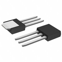
DPAK-3
Case 369D
1 2
TO251-3L POD
B
R
4
E
V
A
1
N
F
SEATING
PLANE
DPAK-3
Case 369D
Style 4
Z
-T-
2
3
F
K
G
J
G
Inches
Max
Min
Max
A
0.213
0.224
5.40
5.70
B
0.252
0.260
6.40
6.60
C
0.087
0.094
2.20
2.40
D
0.024
0.030
0.60
0.75
E
0.022
0.026
0.55
0.65
F
0.022
0.03
0.58
0.091
0.046
0.050
1.18
0.019
0.023
0.49
0.59
K
0.291
0.315
7.40
8.00
N
0.031
0.038
0.78
0.98
R
0.209
0.217
5.30
5.50
0.065
1.35
0.063
Z
0.053
Cathode
2
Anode
3
Gate
4
Anode
0.78
J
S
Pin Assignment
1
2.30
H
V
= Device Code
= M, or N
= Year
= Work Week
= Pb-Free Package
T
Millimeters
Min
G
R12DSx
x
Y
WW
G
R1
2DSxG
YWW
D
3PL
0.13 (0.0005)
H
Dim
R1
2DSxG
YWW
3
C
S
DPAK-3
Case 369C
Style 4
1.28
Ordering Information
1.60
0.150
1. Dimensioning and Tolerancing Per ANSI Y14.5M, 1982.
2. Controlling Dimension: Inch.
STYLE 6:Pin 1. MT1
2. MT2
3. Gate
4. MT2
1.65
Device
Package Type
Package
MCR12DSMT4G
DPAK
369C
MCR12DSN-1G
IPAK
369D
MCR12DSNT4G
DPAK
369C
3.80
Shipping
2500
Tape & Reel
4000 Units/Box
2500
Tape & Reel
Disclaimer Notice - Information furnished is believed to be accurate and reliable. However, users should independently evaluate the suitability of and test each product selected for their own applications. Littelfuse products are
not designed for, and may not be used in, all applications. Read complete Disclaimer Notice at: www.littelfuse.com/disclaimer-electronics
© 2020 Littelfuse, Inc.
Specifications are subject to change without notice.
Revised: 09/09/20
�