NGD8209N
Ignition IGBT 12 A, 410 V
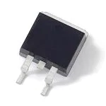
N−Channel DPAK
This Logic Level Insulated Gate Bipolar Transistor (IGBT) features
monolithic circuitry integrating ESD and Over−Voltage clamped
protection for use in inductive coil drivers applications. Primary uses
include motorbike ignition, Direct Fuel Injection, or wherever high
voltage and high current switching is required.
Littelfuse.com
12 AMPS
410 VOLTS
VCE(on) 3 2.0 V @
IC = 6.0 A, VGE . 4.0 V
Features
•
•
•
•
•
•
•
Ideal for Coil−on−Plug Applications
DPAK Package Offers Smaller Footprint and Increased Board Space
Gate−Emitter ESD Protection
Temperature Compensated Gate−Collector Voltage Clamp Limits
Stress Applied to Load
Low Saturation Voltage
High Pulsed Current Capability
These are Pb−Free Devices
C
RG
G
RGE
MAXIMUM RATINGS (TJ = 25°C unless otherwise noted)
Symbol
Value
Unit
Collector−Emitter Voltage
VCES
445
VDC
Collector−Gate Voltage
VCER
445
VDC
Gate−Emitter Voltage
VGE
15
VDC
IC
12
30
ADC
AAC
Rating
Collector Current−Continuous
@ TC = 25°C − Pulsed
ESD (Human Body Model)
R = 1500 Ω, C = 100 pF
ESD
ESD (Machine Model) R = 0 Ω, C = 200 pF
ESD
800
V
PD
94
0.63
Watts
W/°C
TJ, Tstg
−55 to
+175
°C
Total Power Dissipation @ TC = 25°C
Derate above 25°C
Operating and Storage Temperature Range
E
4
1 2
MARKING DIAGRAM
kV
8.0
3
DPAK
CASE 369C
STYLE 7
1
Gate
YWW
NGD
8209G
2
Collector
4
Collector
3
Emitter
Stresses exceeding Maximum Ratings may damage the device. Maximum
Ratings are stress ratings only. Functional operation above the Recommended
Operating Conditions is not implied. Extended exposure to stresses above the
Recommended Operating Conditions may affect device reliability.
Y
= Year
WW = Work Week
G = Pb−Free Device
ORDERING INFORMATION
Specifications subject to change without notice. © 2016 Littelfuse, Inc.
September 19, 2016 − Rev. 0
1
Device
Package
Shipping†
NGD8209NT4G
DPAK
(Pb−Free)
2500 / Tape & Reel
Publication Order Number:
NGD8209N/D
�NGD8209N
UNCLAMPED COLLECTOR−TO−EMITTER AVALANCHE CHARACTERISTICS
Characteristic
Symbol
Single Pulse Collector−to−Emitter Avalanche Energy
VCC = 50 V, VGE = 5.0 V, Pk IL = 7.4 A, L = 10 mH, Starting TJ = 25°C
Value
EAS
Unit
mJ
274
THERMAL CHARACTERISTICS
Characteristic
Symbol
Value
Unit
Thermal Resistance, Junction to Case
RθJC
1.6
°C/W
Thermal Resistance, Junction to Ambient (Note 1)
RθJA
105
TL
275
Maximum Lead Temperature for Soldering Purposes, 1/8″ from case for 5 seconds
°C
1. When surface mounted to an FR4 board using the minimum recommended pad size.
ELECTRICAL CHARACTERISTICS
Characteristic
Symbol
Test Conditions
Temperature
Min
Typ
Max
Unit
BVCES
IC = 2.0 mA
TJ = −40°C to
150°C
380
410
435
VDC
IC = 10 mA
TJ = −40°C to
150°C
390
420
445
TJ = 25°C
−
1.0
25
TJ = 150°C
−
9.0
50
TJ = −40°C
−
0.5
15
TJ = 25°C
−
0.5
1.0
TJ = 150°C
−
10
30
TJ = −40°C
−
0.05
0.5
TJ = 25°C
26
33
38
TJ = 150°C
29
36
41
TJ = −40°C
24
32
36
OFF CHARACTERISTICS
Collector−Emitter Clamp Voltage
Zero Gate Voltage Collector Current
Reverse Collector−Emitter Leakage Current
Reverse Collector−Emitter Clamp Voltage
Gate−Emitter Clamp Voltage
ICES
IECS
BVCES(R)
VCE = 350 V,
VGE = 0 V
VCE = −24 V
IC = −75 mA
μADC
mA
VDC
BVGES
IG = 5.0 mA
TJ = −40°C to
150°C
10
13
16
VDC
IGES
VGE = 10 V
TJ = −40°C to
150°C
380
635
1000
μADC
Gate Resistor
RG
−
TJ = −40°C to
150°C
−
70
−
Ω
Gate Emitter Resistor
RGE
−
TJ = −40°C to
150°C
10
16
26
kΩ
VDC
Gate−Emitter Leakage Current
ON CHARACTERISTICS (Note 2)
Gate Threshold Voltage
VGE(th)
Threshold Temperature Coefficient
(Negative)
IC = 1.0 mA,
VGE = VCE
TJ = 25°C
1.0
1.42
2.0
TJ = 150°C
0.7
0.95
1.5
TJ = −40°C
1.1
1.62
2.2
−
−
−
3.5
−
−
mV/°C
2. Pulse Test: Pulse Width v 300 μS, Duty Cycle v 2%.
Specifications subject to change without notice. © 2016 Littelfuse, Inc.
September 19, 2016 − Rev.0
2
Publication Order Number:
NGD8209N/D
�NGD8209N
ELECTRICAL CHARACTERISTICS (continued)
Symbol
Characteristic
Test Conditions
Temperature
Min
Typ
Max
Unit
TJ = 25°C
0.8
1.45
2.0
VDC
TJ = 150°C
0.85
1.44
1.85
TJ = −40°C
1.0
1.5
1.95
TJ = 25°C
1.1
1.79
2.3
TJ = 150°C
1.2
1.9
2.2
TJ = −40°C
1.3
1.77
2.2
TJ = −40°C to
150°C
5.0
14
30
ON CHARACTERISTICS (continued) (Note 3)
Collector−to−Emitter On−Voltage
VCE(on)
IC = 6.0 A,
VGE = 4.0 V
IC = 10 A,
VGE = 4.5 V
Forward Transconductance
gfs
VCE = 5.0 V, IC = 6.0 A
Mhos
3. Pulse Test: Pulse Width v 300 μS, Duty Cycle v 2%.
TYPICAL CHARACTERISTICS
70
5.0 V
50
IC, COLLECTOR CURRENT (A)
IC, COLLECTOR CURRENT (A)
60
TJ = 25°C
4.0 V
40
30
3.0 V
20
2.5 V
10
0
0
1
2
3
4
5
6
7
8
9
4.0 V
40
30
3.0 V
20
2.5 V
10
0
1
2
3
4
6
7
8
9
VCE, COLLECTOR TO EMITTER VOLTAGE (V)
Figure 1. Output Characteristics
Figure 2. Output Characteristics
30
TJ = 150°C
5.0 V
40
4.0 V
30
3.0 V
20
2.5 V
10
0
5
VCE, COLLECTOR TO EMITTER VOLTAGE (V)
IC, COLLECTOR CURRENT (A)
IC, COLLECTOR CURRENT (A)
5.0 V
TJ = −40°C
50
0
10
50
0
60
1
2
3
4
5
6
7
8
9
150°C
VCE = 10 V
25
25°C
20
15
10
5
0
10
−40°C
0
0.5
1.0
1.5
2.0
2.5
3.0
3.5
4.0
VCE, COLLECTOR TO EMITTER VOLTAGE (V)
VGE, GATE TO EMITTER VOLTAGE (V)
Figure 3. Output Characteristics
Figure 4. Transfer Characteristics
Specifications subject to change without notice. © 2016 Littelfuse, Inc.
September 19, 2016 − Rev. 0
3
10
4.5 5.0
Publication Order Number:
NGD8209N/D
�NGD8209N
2.00
VCE, COLLECTOR TO EMITTER VOLTAGE (V)
VCE, COLLECTOR TO EMITTER VOLTAGE (V)
TYPICAL CHARACTERISTICS
IC = 10 A
1.75
IC = 8 A
1.50
IC = 5 A
1.25
IC = 3 A
1.00
0.75
0.50
0.25
VGE = 5 V
0
−50
−25
25
0
50
75
100
125
150
TJ, JUNCTION TEMPERATURE (°C)
2.00
1.50
IC = 8 A
1.25
IC = 5 A
0.75
0.50
0.25
0
VGE(th), GATE THRESHOLD VOLTAGE (V)
VCE, COLLECTOR TO EMITTER VOLTAGE (V)
1.75
IC = 8 A
1.25
IC = 5 A
1.00
IC = 3 A
0.75
0.50
0.25
0
TJ = 150°C
4
5
6
7
8
9
TJ = 25°C
4
5
6
7
8
9
10
VGE, GATE TO EMITTER VOLTAGE (V)
Figure 6. Collector−to−Emitter Voltage vs.
Gate−to−Emitter Voltage
IC = 10 A
1.50
IC = 3 A
1.00
Figure 5. Collector−to−Emitter Saturation
Voltage vs. Junction Temperature
2.00
IC = 10 A
1.75
10
2.0
1.8
1.6
1.4
1.2
1.0
0.8
0.6
0.4
0.2
0
−50 −30 −10
10
30
50
70
90
110 130 150
VGE, GATE TO EMITTER VOLTAGE (V)
TJ, JUNCTION TEMPERATURE (°C)
Figure 7. Collector−to−Emitter Voltage vs.
Gate−to−Emitter Voltage
Figure 8. Gate Threshold Voltage vs. Junction
Temperature
Specifications subject to change without notice. © 2016 Littelfuse, Inc.
September 19, 2016 − Rev. 0
4
Publication Order Number:
NGD8209N/D
�NGD8209N
PACKAGE DIMENSIONS
DPAK (SINGLE GAUGE)
CASE 369C
ISSUE D
A
E
b3
c2
B
Z
D
1
L4
A
4
L3
b2
2
H
DETAIL A
3
c
b
e
NOTES:
1. DIMENSIONING AND TOLERANCING PER ASME
Y14.5M, 1994.
2. CONTROLLING DIMENSION: INCHES.
3. THERMAL PAD CONTOUR OPTIONAL WITHIN DIMENSIONS b3, L3 and Z.
4. DIMENSIONS D AND E DO NOT INCLUDE MOLD
FLASH, PROTRUSIONS, OR BURRS. MOLD
FLASH, PROTRUSIONS, OR GATE BURRS SHALL
NOT EXCEED 0.006 INCHES PER SIDE.
5. DIMENSIONS D AND E ARE DETERMINED AT THE
OUTERMOST EXTREMES OF THE PLASTIC BODY.
6. DATUMS A AND B ARE DETERMINED AT DATUM
PLANE H.
C
0.005 (0.13)
M
H
C
L2
GAUGE
PLANE
C
L
SEATING
PLANE
A1
L1
DETAIL A
ROTATED 905 CW
DIM
A
A1
b
b2
b3
c
c2
D
E
e
H
L
L1
L2
L3
L4
Z
2.58
0.102
5.80
0.228
3.00
0.118
1.60
0.063
MILLIMETERS
MIN
MAX
2.18
2.38
0.00
0.13
0.63
0.89
0.76
1.14
4.57
5.46
0.46
0.61
0.46
0.61
5.97
6.22
6.35
6.73
2.29 BSC
9.40 10.41
1.40
1.78
2.74 REF
0.51 BSC
0.89
1.27
−−−
1.01
3.93
−−−
STYLE 7:
PIN 1. GATE
2. COLLECTOR
3. EMITTER
4. COLLECTOR
SOLDERING FOOTPRINT*
6.20
0.244
INCHES
MIN
MAX
0.086 0.094
0.000 0.005
0.025 0.035
0.030 0.045
0.180 0.215
0.018 0.024
0.018 0.024
0.235 0.245
0.250 0.265
0.090 BSC
0.370 0.410
0.055 0.070
0.108 REF
0.020 BSC
0.035 0.050
−−− 0.040
0.155
−−−
6.17
0.243
SCALE 3:1
mm Ǔ
ǒinches
Information furnished is believed to be accurate and reliable. However, users should independently evaluate the suitability of and test each product
selected for their own applications. Littelfuse products are not designed for, and shall not be used for, any purpose (including, without limitation,
military, aerospace, medical, life-saving, life-sustaining or nuclear facility applications, devices intended for surgical implant into the body, or any other
application in which the failure or lack of desired operation of the product may result in personal injury, death, or property damage) other than those
expressly set forth in applicable Littelfuse product documentation. Warranties granted by Littelfuse shall be deemed void for products used for any
purpose not expressly set forth in applicable Littelfuse documentation. Littelfuse shall not be liable for any claims or damages arising out of products
used in applications not expressly intended by Littelfuse as set forth in applicable Littelfuse documentation. The sale and use of Littelfuse products
is subject to Littelfuse Terms and Conditions of Sale, unless otherwise agreed by Littelfuse.
Littelfuse.com
Specifications subject to change without notice. © 2016 Littelfuse, Inc.
September 19, 2016 − Rev.
5
Publication Order Number:
NGD8209N/D
�