128K x 36, 256K x 18
3.3V Synchronous SRAMs
3.3V I/O, Pipelined Outputs
Burst Counter, Single Cycle Deselect
Features
◆
◆
◆
◆
◆
◆
◆
◆
◆
IDT71V3576S
IDT71V3578S
IDT71V3576SA
IDT71V3578SA
Description
128K x 36, 256K x 18 memory configurations
Supports high system speed:
Commercial and Industrial:
– 150MHz 3.8ns clock access time
– 133MHz 4.2ns clock access time
LBO input selects interleaved or linear burst mode
Self-timed write cycle with global write control (GW), byte write
enable (BWE), and byte writes (BWx)
3.3V core power supply
Power down controlled by ZZ input
3.3V I/O
Optional - Boundary Scan JTAG Interface (IEEE 1149.1
compliant)
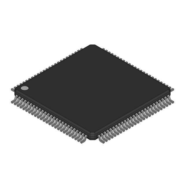
Packaged in a JEDEC Standard 100-pin plastic thin quad
flatpack (TQFP), 119 ball grid array (BGA) and 165 fine pitch ball
grid array (fBGA)
The IDT71V3576/78 are high-speed SRAMs organized as
128K x 36/256K x 18. The IDT71V3576/78 SRAMs contain write, data,
address and control registers. Internal logic allows the SRAM to generate
a self-timed write based upon a decision which can be left until the end of
the write cycle.
The burst mode feature offers the highest level of performance to the
system designer, as the IDT71V3576/78 can provide four cycles of data
for a single address presented to the SRAM. An internal burst address
counter accepts the first cycle address from the processor, initiating the
access sequence. The first cycle of output data will be pipelined for one
cycle before it is available on the next rising clock edge. If burst mode
operation is selected (ADV=LOW), the subsequent three cycles of output
data will be available to the user on the next three rising clock edges. The
order of these three addresses are defined by the internal burst counter
and the LBO input pin.
The IDT71V3576/78 SRAMs utilize IDT’s latest high-performance
CMOS process and are packaged in a JEDEC standard 14mm x 20mm
100-pin thin plastic quad flatpack (TQFP) as well as a 119 ball grid array
(BGA) and a 165 fine pitch ball grid array (fBGA).
Pin Description Summary
A0-A17
Address Inputs
Input
Synchronous
CE
Chip Enable
Input
Synchronous
CS0, CS1
Chip Selects
Input
Synchronous
OE
Output Enable
Input
Asynchronous
GW
Global Write Enable
Input
Synchronous
Byte Write Enable
Input
Synchronous
BW1, BW2, BW3, BW4
Individual Byte Write Selects
Input
Synchronous
CLK
Clock
Input
N/A
ADV
Burst Address Advance
Input
Synchronous
ADSC
Address Status (Cache Controller)
Input
Synchronous
ADSP
Address Status (Processor)
Input
Synchronous
LBO
Linear / Interleaved Burst Order
Input
DC
TMS
Test Mode Select
Input
Synchronous
TDI
Test Data Input
Input
Synchronous
TCK
Test Clock
Input
N/A
TDO
Test Data Output
Output
Synchronous
TRST
JTAG Reset (Optional)
Input
Asynchronous
ZZ
Sleep Mode
Input
Asynchronous
I/O0-I/O31, I/OP1-I/OP4
Data Input / Output
I/O
Synchronous
VDD, VDDQ
Core Power, I/O Power
Supply
N/A
VSS
Ground
Supply
N/A
BWE
(1)
5279 tbl 01
NOTE:
1. BW3 and BW4 are not applicable for the IDT71V3578.
JANUARY 2004
1
©2004 Integrated Device Technology, Inc.
DSC-5279/04
�IDT71V3576, IDT71V3578, 128K x 36, 256K x 18, 3.3V Synchronous SRAMs with
3.3V I/O, Pipelined Outputs, Burst Counter, Single Cycle Deselect
Commercial and Industrial Temperature Ranges
Pin Definitions(1)
Symbol
Pin Function
I/O
Active
Description
A0-A17
Address Inputs
I
N/A
Synchronous Address inputs. The address register is triggered by a combination of the rising edge
of CLK and ADSC Low or ADSP Low and CE Low.
ADSC
Address Status
(Cache Controller)
I
LOW
Synchronous Address Status from Cache Controller. ADSC is an active LOW input that is used to load
the address registers with new addresses.
ADSP
Address Status
(Processor)
I
LOW
Synchronous Address Status from Processor. ADSP is an active LOW input that is used to load the
address registers with new addresses. ADSP is gated by CE.
ADV
Burst Address
Advance
I
LOW
Synchronous Address Advance. ADV is an active LOW input that is used to advance the internal burst
counter, controlling burst access after the initial address is loaded. When the input is HIGH the burst
counter is not incremented; that is, there is no address advance.
BWE
Byte Write Enable
I
LOW
Synchronous byte write enable gates the byte write inputs BW1-BW4. If BWE is LOW at the rising
edge of CLK then BWx inputs are passed to the next stage in the circuit. If BWE is HIGH then the
byte write inputs are blocked and only GW can initiate a write cycle.
BW1-BW4
Individual Byte
Write Enables
I
LOW
Synchronous byte write enables. BW1 controls I/O0-7, I/OP1, BW2 controls I/O8-15, I/OP2, etc. Any active
byte write causes all outputs to be disabled.
CE
Chip Enable
I
LOW
Synchronous chip enable. CE is used with CS 0 and CS1 to enable the IDT71V3576/78. CE also gates
ADSP.
CLK
Clock
I
N/A
This is the clock input. All timing references for the device are made with respect to this input.
CS0
Chip Select 0
I
HIGH
Synchronous active HIGH chip select. CS0 is used with CE and CS1 to enable the chip.
CS1
Chip Select 1
I
LOW
Synchronous active LOW chip select. CS1 is used with CE and CS0 to enable the chip.
GW
Global Write
Enable
I
LOW
Synchronous global write enable. This input will write all four 9-bit data bytes when LOW on the rising
edge of CLK. GW supersedes individual byte write enables.
I/O0-I/O31
I/OP1-I/OP4
Data Input/Output
I/O
N/A
Synchronous data input/output (I/O) pins. Both the data input path and data output path are registered
and triggered by the rising edge of CLK.
LBO
Linear Burst Order
I
LOW
Async hronous burst order selection input. When LBO is HIGH, the interleaved burst sequence is
selected. When LBO is LOW the Linear burst sequence is selected. LBO is a static input and must
not change state while the device is operating.
OE
Output Enable
I
LOW
Asynchronous output enable. When OE is LOW the data output drivers are enabled on the I/O pins if
the chip is also selected. When OE is HIGH the I/O pins are in a high-impedance state.
TMS
Test ModeSelect
I
N/A
Gives input command for TAP controller. Sampled on rising edge of TDK. This pin has an internal
pullup.
TDI
Test Data Input
I
N/A
Serial input of registers placed between TDI and TDO. Sampled on rising edge of TCK. This pin has
an internal pullup.
TCK
Test Clock
I
N/A
Clock input of TAP controller. Each TAP event is clocked. Test inputs are captured on rising edge of
TCK, while test outputs are driven from the falling edge of TCK. This pin has an internal pullup.
TDO
Test DataOutput
O
N/A
Serial output of registers placed between TDI and TDO. This output is active depending on the state
of the TAP controller.
TRST
JTAG Reset
(Optional)
I
LOW
Optional Asynchrono us JTAG reset. Can be used to reset the TAP controller, but not required. JTAG
reset occurs automatically at power up and also resets using TMS and TCK per IEEE 1149.1. If not
used TRST can be left floating. This pin has an internal pullup. Only available in BGA package.
ZZ
Sleep Mode
I
HIGH
Asynchronous sleep mode input. ZZ HIGH will gate the CLK internally and power down the
IDT71V3576/78 to its lowest power consumption level. Data retention is guaranteed in Sleep
Mode.This pin has an internal pull down.
VDD
Power Supply
N/A
N/A
3.3V core power supply.
VDDQ
Power Supply
N/A
N/A
3.3V I/O Supply.
VSS
Ground
N/A
N/A
Ground.
NC
No Connect
N/A
N/A
NC pins are not electrically connected to the device.
5279 tbl 02
NOTE:
1. All synchronous inputs must meet specified setup and hold times with respect to CLK.
6.42
2
�IDT71V3576, IDT71V3578, 128K x 36, 256K x 18, 3.3V Synchronous SRAMs with
3.3V I/O, Pipelined Outputs, Burst Counter, Single Cycle Deselect
Commercial and Industrial Temperature Ranges
Functional Block Diagram
LBO
ADV
CLK
2
Binary
Counter
ADSC
Burst
Logic
Q0
CLR
ADSP
Q1
CLK EN
ADDRESS
REGISTER
A0 - A16/17
GW
BWE
INTERNAL
ADDRESS
Burst
Sequence
CEN
17/18
A0*
A1*
128K x 36/
256K x 18BIT
MEMORY
ARRAY
2
A0,A1
A2–A17
36/18
17/18
Byte 1
Write Register
36/18
Byte 1
Write Driver
BW1
9
Byte 2
Write Register
Byte 2
Write Driver
BW2
9
Byte 3
Write Register
Byte 3
Write Driver
BW3
9
Byte 4
Write Register
Byte 4
Write Driver
BW4
9
OUTPUT
REGISTER
CE
CS0
CS1
D
Q
Enable
Register
DATA INPUT
REGISTER
CLK EN
ZZ
Powerdown
D
Q
Enable
Delay
Register
OE
OE
I/O0 — I/O31
I/OP1 — I/OP4
OUTPUT
BUFFER
36/18
5279 drw 01
TMS
TDI
TCK
TRST
(Optional)
JTAG
(SA Version)
TDO
6.42
3
,
�IDT71V3576, IDT71V3578, 128K x 36, 256K x 18, 3.3V Synchronous SRAMs with
3.3V I/O, Pipelined Outputs, Burst Counter, Single Cycle Deselect
Commercial and Industrial Temperature Ranges
Absolute Maximum Ratings(1)
Symbol
Rating
Recommended Operating
Temperature and Supply Voltage
Commercial &
Industrial
Unit
Grade
Temperature(1)
VSS
VDD
V DDQ
Commercial
0°C to +70°C
0V
3.3V±5%
3.3V±5%
Industrial
-40°C to +85°C
0V
3.3V±5%
3.3V±5%
VTERM(2)
Terminal Voltage with
Respect to GND
-0.5 to +4.6
V
VTERM(3,6)
Terminal Voltage with
Respect to GND
-0.5 to VDD
V
VTERM(4,6)
Terminal Voltage with
Respect to GND
-0.5 to VDD +0.5
V
VTERM(5,6)
Terminal Voltage with
Respect to GND
-0.5 to VDDQ +0.5
V
Commercial
Operating Temperature
-0 to +70
o
C
Industrial
Operating Temperature
-40 to +85
o
C
Temperature
Under Bias
-55 to +125
o
TA
(7)
TBIAS
TSTG
Recommended DC Operating
Conditions
Symbol
C
o
-55 to +125
2.0
W
IOUT
DC Output Current
50
mA
Typ.
Max.
Unit
3.135
3.3
3.465
V
VDDQ
I/O Supply Voltage
3.135
3.3
3.465
V
VSS
Supply Voltage
0
0
0
V
2.0
____
VDD +0.3
2.0
____
VIH
VIL
Power Dissipation
Min.
Core Supply Voltage
C
PT
Parameter
VDD
VIH
Storage
Temperature
5279 tbl 04
NOTES:
1. TA is the "instant on" case temperature.
Input High Voltage - Inputs
Input High Voltage - I/O
Input Low Voltage
-0.3
(2)
____
V
(1)
VDDQ +0.3
0.8
V
V
5279 tbl 06
NOTES:
1. VIH (max) = VDDQ + 1.0V for pulse width less than tCYC/2, once per cycle.
2. VIL (min) = -1.0V for pulse width less than tCYC/2, once per cycle.
5279 tbl 03
NOTES:
1. Stresses greater than those listed under ABSOLUTE MAXIMUM RATINGS may
cause permanent damage to the device. This is a stress rating only and functional
operation of the device at these or any other conditions above those indicated
in the operational sections of this specification is not implied. Exposure to absolute
maximum rating conditions for extended periods may affect reliability.
2. VDD terminals only.
3. VDDQ terminals only.
4. Input terminals only.
5. I/O terminals only.
6. This is a steady-state DC parameter that applies after the power supplies have
ramped up. Power supply sequencing is not necessary; however, the voltage
on any input or I/O pin cannot exceed V DDQ during power supply ramp up.
7. TA is the "instant on" case temperature.
100 Pin TQFP Capacitance
119 BGA Capacitance
(TA = +25°C, f = 1.0MHz)
Symbol
Parameter
(1)
CIN
Input Capacitance
CI/O
I/O Capacitance
(TA = +25°C, f = 1.0MHz)
Max.
Unit
Symbol
VIN = 3dV
5
pF
CIN
Input Capacitance
VOUT = 3dV
7
pF
CI/O
I/O Capacitance
165 fBGA Capacitance
5279 tbl 07
(TA = +25°C, f = 1.0MHz)
Symbol
Parameter(1)
CIN
Input Capacitance
CI/O
I/O Capacitance
Parameter(1)
Conditions
Conditions
Max.
Unit
VIN = 3dV
7
pF
VOUT = 3dV
7
pF
5279 tbl 07b
NOTE:
1. This parameter is guaranteed by device characterization, but not production tested.
6.42
4
Conditions
Max.
Unit
VIN = 3dV
7
pF
VOUT = 3dV
7
pF
5279 tbl 07a
�IDT71V3576, IDT71V3578, 128K x 36, 256K x 18, 3.3V Synchronous SRAMs with
3.3V I/O, Pipelined Outputs, Burst Counter, Single Cycle Deselect
Commercial and Industrial Temperature Ranges
A6
A7
CE
CS0
BW4
BW3
BW2
BW1
CS1
VDD
VSS
CLK
GW
BWE
OE
ADSC
ADSP
ADV
A8
A9
Pin Configuration – 128K x 36
100 99 98 97 96 95 94 93 92 91 90 89 88 87 86 85 84 83 82 81
I/OP3
I/O16
I/O17
VDDQ
VSS
I/O18
I/O19
I/O20
I/O21
VSS
VDDQ
I/O22
I/O23
VDD / NC(1)
VDD
NC
VSS
I/O24
I/O25
VDDQ
VSS
I/O26
I/O27
I/O28
I/O29
VSS
VDDQ
I/O30
I/O31
I/OP4
1
80
2
79
3
4
78
77
5
76
6
75
7
74
8
73
9
72
71
10
11
70
12
69
13
68
14
67
15
66
16
65
64
17
18
19
63
62
20
61
21
60
22
59
23
24
58
57
25
56
26
55
27
54
28
53
29
52
30
51
I/OP2
I/O15
I/O14
VDDQ
VSS
I/O13
I/O12
I/O11
I/O10
VSS
VDDQ
I/O9
I/O8
VSS
NC
VDD
ZZ(2)
I/O7
I/O6
VDDQ
VSS
I/O5
I/O4
I/O3
I/O2
VSS
VDDQ
I/O1
I/O0
I/OP1
31 32 33 34 35 36 37 38 39 40 41 42 43 44 45 46 47 48 49 50
NC
NC
VSS
VDD
NC
NC
A10
A11
A12
A13
A14
A15
A16
LBO
A5
A4
A3
A2
A1
A0
5279 drw 02
TQFP
Top View
NOTES:
1. Pin 14 can either be directly connected to VDD, or connected to an input voltage ≥ VIH, or left unconnected.
2. Pin 64 can be left unconnected and the device will always remain in active mode.
6.42
5
,
�IDT71V3576, IDT71V3578, 128K x 36, 256K x 18, 3.3V Synchronous SRAMs with
3.3V I/O, Pipelined Outputs, Burst Counter, Single Cycle Deselect
Commercial and Industrial Temperature Ranges
A6
A7
CE
CS0
NC
NC
BW2
BW1
CS1
VDD
VSS
CLK
GW
BWE
OE
ADSC
ADSP
ADV
A8
A9
Pin Configuration – 256K x 18
100 99 98 97 96 95 94 93 92 91 90 89 88 87 86 85 84 83 82 81
NC
NC
NC
1
80
2
79
3
VDDQ
VSS
NC
NC
I/O8
I/O9
VSS
VDDQ
I/O10
I/O11
VDD / NC(1)
VDD
NC
VSS
I/O12
I/O13
VDDQ
VSS
I/O14
I/O15
I/OP2
NC
VSS
VDDQ
NC
NC
NC
4
78
77
5
76
6
75
7
74
8
73
9
72
71
10
11
70
12
69
13
68
14
67
15
66
16
65
17
64
18
63
19
62
20
61
21
60
22
59
23
58
24
57
25
56
26
55
27
28
54
53
29
52
51
30
A10
NC
NC
VDDQ
VSS
NC
I/OP1
I/O7
I/O6
VSS
VDDQ
I/O5
I/O4
VSS
NC
VDD
ZZ(2)
I/O3
I/O2
VDDQ
VSS
I/O1
I/O0
NC
NC
VSS
VDDQ
NC
NC
NC
31 32 33 34 35 36 37 38 39 40 41 42 43 44 45 46 47 48 49 50
LBO
A5
A4
A3
A2
A1
A0
NC
NC
VSS
VDD
NC
NC
A11
A12
A13
A14
A15
A16
A17
5279 drw 03
TQFP
Top View
NOTES:
1. Pin 14 can either be directly connected to VDD, or connected to an input voltage ≥ VIH, or left unconnected.
2. Pin 64 can be left unconnected and the device will always remain in active mode.
6.42
6
,
�IDT71V3576, IDT71V3578, 128K x 36, 256K x 18, 3.3V Synchronous SRAMs with
3.3V I/O, Pipelined Outputs, Burst Counter, Single Cycle Deselect
Commercial and Industrial Temperature Ranges
Pin Configuration – 128K x 36, 119 BGA
1
2
3
4
5
6
7
A
VDDQ
A6
A4
ADSP
A8
A16
VDDQ
B
NC
CS0
A3
ADSC
A9
CS1
NC
C
NC
A7
A2
VDD
A12
A15
NC
D
I/O16
I/OP3
VSS
NC
VSS
I/OP2
I/O15
E
I/O17
I/O18
VSS
CE
VSS
I/O13
I/O14
F
VDDQ
I/O19
VSS
OE
VSS
I/O12
VDDQ
G
I/O20
I/O21
BW3
ADV
BW 2
I/O11
I/O10
H
I/O22
I/O23
VSS
GW
VSS
I/O9
I/O8
J
VDDQ
VDD
NC
VDD
NC
VDD
VDDQ
K
I/O24
I/O26
VSS
CLK
VSS
I/O6
I/O7
L
I/O25
I/O27
BW4
NC
BW1
I/O4
I/O5
M
VDDQ
I/O28
VSS
BWE
VSS
I/O3
VDDQ
N
I/O29
I/O30
VSS
A1
VSS
I/O2
I/O1
P
I/O31
I/OP4
VSS
A0
VSS
R
NC
A5
LBO
VDD
T
NC
NC
A10
A11
A14
VDDQ
NC/TMS(2)
NC/TDI(2)
NC/TCK(2)
NC/TDO(2)
U
V DD / NC(1)
I/O0
I/OP1
A13
NC
NC
ZZ(4)
NC/TRST(2,3)
Top View
,
VDDQ
5279 drw 04
Pin Configuration – 256K x 18, 119 BGA
1
2
3
4
5
6
7
A
VDDQ
A6
A4
ADSP
A8
A16
VDDQ
B
NC
CS0
A3
ADSC
A9
CS1
NC
C
NC
A7
A2
VDD
A13
A17
NC
D
I/O8
NC
VSS
NC
VSS
I/O7
NC
E
NC
I/O9
VSS
CE
VSS
NC
I/O6
VSS
OE
VSS
I/O5
VDDQ
NC
I/O4
F
VDDQ
NC
G
NC
I/O10
BW2
ADV
VSS
H
I/O11
NC
VSS
GW
VSS
I/O3
NC
J
VDDQ
VDD
NC
VDD
NC
VDD
VDDQ
K
NC
I/O12
VSS
CLK
VSS
NC
I/O2
L
I/O13
NC
VSS
NC
BW1
I/O1
NC
M
VDDQ
I/O14
VSS
BWE
VSS
NC
VDDQ
N
I/O15
NC
VSS
A1
VSS
I/O0
NC
P
NC
I/OP2
VSS
A0
VSS
NC
I/OP1
R
NC
A5
LBO
VDD
A12
NC
T
NC
A10
A15
NC
A11
ZZ(4)
U
VDDQ
NC/TMS(2) NC/TDI(2) NC/TCK(2)
VDD / NC(1)
A14
,
NC/TDO(2) NC/TRST(2,3) VDDQ
Top View
5279 drw 05
NOTES:
1. R5 can either be directly connected to VDD, or connected to an input voltage ≥ VIH, or left unconnected.
2. These pins are NC for the "S" version or the JTAG signal listed for the "SA" version. Note: If NC, these pins can either be tied to VSS , VDD or left floating.
3. TRST is offered as an optional JTAG Reset if required in the application. If not needed, can be left floating and will internally be pulled to VDD.
4. T7 can be left unconnected and the device will always remain in active mode.
6.42
7
�IDT71V3576, IDT71V3578, 128K x 36, 256K x 18, 3.3V Synchronous SRAMs with
3.3V I/O, Pipelined Outputs, Burst Counter, Single Cycle Deselect
Commercial and Industrial Temperature Ranges
Pin Configuration – 128K x 36, 165 fBGA
1
2
3
4
5
6
7
8
9
10
11
A
NC(2)
A7
CE1
BW3
BW2
CS1
BWE
ADSC
ADV
A8
NC
B
NC
A6
CS0
BW4
BW1
CLK
GW
OE
ADSP
A9
NC(2)
C
I/OP3
NC
VDDQ
VSS
VSS
VSS
VSS
VSS
VDDQ
NC
I/OP2
D
I/O17
I/O16
VDDQ
VDD
VSS
VSS
VSS
VDD
VDDQ
I/O15
I/O14
E
I/O19
I/O18
VDDQ
VDD
VSS
VSS
VSS
VDD
VDDQ
I/O13
I/O12
F
I/O21
I/O20
VDDQ
VDD
VSS
VSS
VSS
VDD
VDDQ
I/O11
I/O10
G
I/O23
I/O22
VDDQ
VDD
VSS
VSS
VSS
VDD
VDDQ
I/O9
I/O8
H
VDD
(1)
NC
NC
VDD
VSS
VSS
VSS
VDD
NC
NC
ZZ(5)
J
I/O25
I/O24
VDDQ
VDD
VSS
VSS
VSS
VDD
VDDQ
I/O7
I/O6
K
I/O27
I/O26
VDDQ
VDD
VSS
VSS
VSS
VDD
VDDQ
I/O5
I/O4
L
I/O29
I/O28
VDDQ
VDD
VSS
VSS
VSS
VDD
VDDQ
I/O3
I/O2
M
I/O31
I/O30
VDDQ
VDD
VSS
VSS
VSS
VDD
VDDQ
I/O1
I/O0
NC
VSS
VDDQ
NC
I/OP1
(3, 4)
(2)
N
I/OP4
NC
VDDQ
VSS
P
NC
NC(2)
A5
A2
NC/TDI(3)
A1
NC/TDO(3)
A10
A13
A14
NC(2)
R
LBO
NC(2)
A4
A3
NC/TMS(3)
A0
NC/TCK(3)
A11
A12
A15
A16
NC/TRST
NC
5279 tbl 17
Pin Configuration – 256K x 18, 165 fBGA
1
2
3
4
5
6
7
8
9
10
11
A
NC
A7
CE1
BW2
NC
CS1
BWE
ADSC
ADV
A8
A10
B
NC
A6
CS0
NC
BW1
CLK
GW
OE
ADSP
A9
NC(2)
C
NC
NC
VDDQ
VSS
VSS
VSS
VSS
VSS
VDDQ
NC
I/OP1
D
NC
I/O8
VDDQ
VDD
VSS
VSS
VSS
VDD
VDDQ
NC
I/O7
E
NC
I/O9
VDDQ
VDD
VSS
VSS
VSS
VDD
VDDQ
NC
I/O6
F
NC
I/O10
VDDQ
VDD
VSS
VSS
VSS
VDD
VDDQ
NC
I/O5
G
NC
(2)
I/O11
VDDQ
VDD
VSS
VSS
VSS
VDD
VDDQ
NC
I/O4
H
(1)
VDD
NC
NC
VDD
VSS
VSS
VSS
VDD
NC
NC
ZZ(5)
J
I/O12
NC
VDDQ
VDD
VSS
VSS
VSS
VDD
VDDQ
I/O3
NC
K
I/O13
NC
VDDQ
VDD
VSS
VSS
VSS
VDD
VDDQ
I/O2
NC
L
I/O14
NC
VDDQ
VDD
VSS
VSS
VSS
VDD
VDDQ
I/O1
NC
M
I/O15
NC
VDDQ
VDD
VSS
VSS
VSS
VDD
VDDQ
I/O0
NC
NC
NC
VSS
VDDQ
NC
NC
(3, 4)
(2)
N
I/OP2
NC
VDDQ
VSS
P
NC
NC(2)
A5
A2
NC/TDI(3)
A1
NC/TDO(3)
A11
A14
A15
NC(2)
R
LBO
NC(2)
A4
A3
NC/TMS(3)
A0
NC/TCK (3)
A12
A13
A16
A17
NC/TRST
5279 tbl 17a
NOTES:
1. H1 can either be directly connected to VDD, or connected to an input voltage ≥ VIH, or left unconnected.
2. Pins P11, N6, B11, A1, R2 and P2 are reserved for 9M, 18M, 36M, 72M, 144M and 288M respectively.
3. These pins are NC for the "S" version or the JTAG signal listed for the "SA" version. Note: If NC, these pins can either be tied to VSS, VDD or left floating.
4. TRST is offered as an optional JTAG reset if required in the application. If not needed, can be left floating and will internally be pulled to VDD.
5. H11 can be left unconnected and the device will always remain in active mode.
6.42
8
�IDT71V3576, IDT71V3578, 128K x 36, 256K x 18, 3.3V Synchronous SRAMs with
3.3V I/O, Pipelined Outputs, Burst Counter, Single Cycle Deselect
Commercial and Industrial Temperature Ranges
DC Electrical Characteristics Over the Operating
Temperature and Supply Voltage Range (VDD = 3.3V ± 5%)
Symbol
Parameter
Test Conditions
Min.
Max.
Unit
5
µA
|ILI|
Input Leakage Current
VDD = Max., VIN = 0V to V DD
___
|ILZZ|
ZZ, LBO and JTAG Input Leakage Current(1)
VDD = Max., VIN = 0V to V DD
___
30
µA
VOUT = 0V to V DDQ , Device Deselected
___
5
µA
IOL = +8mA, VDD = Min.
___
0.4
V
2.4
___
V
|ILO|
Output Leakage Current
Output Low Voltage
VOL
Output High Voltage
VOH
IOH = -8mA, VDD = Min.
5279 tbl 08
NOTE:
1. The LBO, TMS, TDI, TCK and TRST pins will be internally pulled to VDD and the ZZ pin will be internally pulled to V SS if they are not actively driven in the application.
DC Electrical Characteristics Over the Operating
Temperature and Supply Voltage Range(1)
150MHz
Symbol
Parameter
Test Conditions
133MHz
Com'l
Ind
Com'l
Ind
Unit
IDD
Operating Power Supply
Current
Device Selected, Outputs Open, VDD = Max.,
VDDQ = Max., VIN > VIH or < VIL, f = fMAX(2)
295
305
250
260
mA
ISB1
CMOS Standby Power
Supply Current
Device Deselected, Outputs Open, V DD = Max.,
VDDQ = Max., VIN > VHD or < VLD, f = 0(2,3)
30
35
30
35
mA
ISB2
Clock Running Power
Supply Current
Device Deselected, Outputs Open, V DD = Max.,
VDDQ = Max., VIN > VHD or < VLD, f = fMAX(2,3)
105
115
100
110
mA
IZZ
Full Sleep Mode Supply
Current
ZZ > VHD, VDD = Max.
30
35
30
35
mA
5279 tbl 09
NOTES:
1. All values are maximum guaranteed values.
2. At f = fMAX, inputs are cycling at the maximum frequency of read cycles of 1/tCYC while ADSC = LOW; f=0 means no input lines are changing.
3. For I/Os VHD = VDDQ - 0.2V, VLD = 0.2V. For other inputs VHD = V DD - 0.2V, VLD = 0.2V.
AC Test Conditions
AC Test Load
(VDDQ = 3.3V)
Input Pulse Levels
VDDQ/2
50Ω
0 to 3V
I/O
Input Rise/Fall Times
2ns
Input Timing Reference Levels
1.5V
Output Timing Reference Levels
1.5V
6
See Figure 1
5
Z0 = 50Ω
5279 drw 06
AC Test Load
,
Figure 1. AC Test Load
5279 tbl 10
4
∆tCD 3
(Typical, ns)
2
1
20 30 50
80 100
Capacitance (pF)
Figure 2. Lumped Capacitive Load, Typical Derating
6.42
9
200
5279 drw 07
,
�IDT71V3576, IDT71V3578, 128K x 36, 256K x 18, 3.3V Synchronous SRAMs with
3.3V I/O, Pipelined Outputs, Burst Counter, Single Cycle Deselect
Commercial and Industrial Temperature Ranges
Synchronous Truth Table(1,3)
Address
Used
CE
CS0
CS1
ADSP
ADSC
ADV
GW
BWE
BWx
OE
(2)
CLK
I/O
Deselected Cycle, Power Down
None
H
X
X
X
L
X
X
X
X
X
-
HI-Z
Deselected Cycle, Power Down
None
L
X
H
L
X
X
X
X
X
X
-
HI-Z
Deselected Cycle, Power Down
None
L
L
X
L
X
X
X
X
X
X
-
HI-Z
Deselected Cycle, Power Down
None
L
X
H
X
L
X
X
X
X
X
-
HI-Z
Deselected Cycle, Power Down
None
L
L
X
X
L
X
X
X
X
X
-
HI-Z
Read Cycle, Begin Burst
External
L
H
L
L
X
X
X
X
X
L
-
DOUT
Read Cycle, Begin Burst
External
L
H
L
L
X
X
X
X
X
H
-
HI-Z
Read Cycle, Begin Burst
External
L
H
L
H
L
X
H
H
X
L
-
DOUT
Read Cycle, Begin Burst
External
L
H
L
H
L
X
H
L
H
L
-
DOUT
Read Cycle, Begin Burst
External
L
H
L
H
L
X
H
L
H
H
-
HI-Z
Write Cycle, Begin Burst
External
L
H
L
H
L
X
H
L
L
X
-
DIN
Write Cycle, Begin Burst
External
L
H
L
H
L
X
L
X
X
X
-
DIN
Read Cycle, Continue Burst
Next
X
X
X
H
H
L
H
H
X
L
-
DOUT
Read Cycle, Continue Burst
Next
X
X
X
H
H
L
H
H
X
H
-
HI-Z
Read Cycle, Continue Burst
Next
X
X
X
H
H
L
H
X
H
L
-
DOUT
Read Cycle, Continue Burst
Next
X
X
X
H
H
L
H
X
H
H
-
HI-Z
Read Cycle, Continue Burst
Next
H
X
X
X
H
L
H
H
X
L
-
DOUT
Read Cycle, Continue Burst
Next
H
X
X
X
H
L
H
H
X
H
-
HI-Z
Read Cycle, Continue Burst
Next
H
X
X
X
H
L
H
X
H
L
-
DOUT
Read Cycle, Continue Burst
Next
H
X
X
X
H
L
H
X
H
H
-
HI-Z
Write Cycle, Continue Burst
Next
X
X
X
H
H
L
H
L
L
X
-
DIN
Write Cycle, Continue Burst
Next
X
X
X
H
H
L
L
X
X
X
-
DIN
Write Cycle, Continue Burst
Next
H
X
X
X
H
L
H
L
L
X
-
DIN
Write Cycle, Continue Burst
Next
H
X
X
X
H
L
L
X
X
X
-
DIN
Read Cycle, Suspend Burst
Current
X
X
X
H
H
H
H
H
X
L
-
DOUT
Read Cycle, Suspend Burst
Current
X
X
X
H
H
H
H
H
X
H
-
HI-Z
Read Cycle, Suspend Burst
Current
X
X
X
H
H
H
H
X
H
L
-
DOUT
Read Cycle, Suspend Burst
Current
X
X
X
H
H
H
H
X
H
H
-
HI-Z
Read Cycle, Suspend Burst
Current
H
X
X
X
H
H
H
H
X
L
-
DOUT
Read Cycle, Suspend Burst
Current
H
X
X
X
H
H
H
H
X
H
-
HI-Z
Read Cycle, Suspend Burst
Current
H
X
X
X
H
H
H
X
H
L
-
DOUT
Read Cycle, Suspend Burst
Current
H
X
X
X
H
H
H
X
H
H
-
HI-Z
Write Cycle, Suspend Burst
Current
X
X
X
H
H
H
H
L
L
X
-
DIN
Write Cycle, Suspend Burst
Current
X
X
X
H
H
H
L
X
X
X
-
DIN
Write Cycle, Suspend Burst
Current
H
X
X
X
H
H
H
L
L
X
-
DIN
Write Cycle, Suspend Burst
Current
H
X
X
X
H
H
L
X
X
X
-
DIN
Operation
5279 tbl 11
NOTES:
1. L = VIL, H = VIH, X = Don’t Care.
2. OE is an asynchronous input.
3. ZZ = low for this table.
6.42
10
�IDT71V3576, IDT71V3578, 128K x 36, 256K x 18, 3.3V Synchronous SRAMs with
3.3V I/O, Pipelined Outputs, Burst Counter, Single Cycle Deselect
Commercial and Industrial Temperature Ranges
Synchronous Write Function Truth Table(1, 2)
Operation
GW
BWE
BW1
BW2
BW3
BW4
Read
H
H
X
X
X
X
Read
H
L
H
H
H
H
Write all Bytes
L
X
X
X
X
X
Write all Bytes
H
L
L
L
L
L
(3)
H
L
L
H
H
H
(3)
H
L
H
L
H
H
(3)
H
L
H
H
L
H
(3)
H
L
H
H
H
L
Write Byte 1
Write Byte 2
Write Byte 3
Write Byte 4
5279 tbl 12
NOTES:
1. L = VIL, H = V IH, X = Don’t Care.
2. BW3 and BW4 are not applicable for the IDT71V3578.
3. Multiple bytes may be selected during the same cycle.
Asynchronous Truth Table(1)
Operation(2)
OE
ZZ
I/O Status
Power
Read
L
L
Data Out
Active
Read
H
L
High-Z
Active
Write
X
L
High-Z – Data In
Active
Deselected
X
L
High-Z
Standby
Sleep Mode
X
H
High-Z
Sleep
5279 tbl 13
NOTES:
1. L = VIL, H = V IH, X = Don’t Care.
2. Synchronous function pins must be biased appropriately to satisfy operation requirements.
Interleaved Burst Sequence Table (LBO=VDD)
Sequence 1
Sequence 2
Sequence 3
Sequence 4
A1
A0
A1
A0
A1
A0
A1
A0
First Address
0
0
0
1
1
0
1
1
Second Address
0
1
0
0
1
1
1
0
Third Address
1
0
1
1
0
0
0
1
1
1
1
0
0
1
0
Fourth Address
(1)
0
5279 tbl 14
NOTE:
1. Upon completion of the Burst sequence the counter wraps around to its initial state.
Linear Burst Sequence Table (LBO=VSS)
Sequence 1
Sequence 2
Sequence 3
Sequence 4
A1
A0
A1
A0
A1
A0
A1
A0
First Address
0
0
0
1
1
0
1
1
Second Address
0
1
1
0
1
1
0
0
Third Address
1
0
1
1
0
0
0
1
Fourth Address(1)
1
1
0
0
0
1
1
0
NOTE:
1. Upon completion of the Burst sequence the counter wraps around to its initial state.
6.42
11
5279 tbl 15
�IDT71V3576, IDT71V3578, 128K x 36, 256K x 18, 3.3V Synchronous SRAMs with
3.3V I/O, Pipelined Outputs, Burst Counter, Single Cycle Deselect
Commercial and Industrial Temperature Ranges
AC Electrical Characteristics
(VDD = 3.3V ±5%, Commercial and Industrial Temperature Ranges)
150MHz
Symbol
Parameter
133MHz
Min.
Max.
Min.
Max.
Unit
tCYC
Clock Cycle Time
6.7
____
7.5
____
ns
tCH(1)
Clock High Pulse Width
2.6
____
3
____
ns
tCL(1)
Clock Low Pulse Width
2.6
____
3
____
ns
____
3.8
____
4.2
ns
1.5
____
ns
Output Parameters
tCD
Clo ck High to Valid Data
tCDC
Clock High to Data Change
1.5
____
tCLZ(2)
Clock High to Output Active
0
____
0
____
ns
tCHZ(2)
Clock High to Data High-Z
1.5
3.8
1.5
4.2
ns
tOE
Output Enable Access Time
____
3.8
____
4.2
ns
tOLZ(2)
Output Enable Low to Output Active
0
____
0
____
ns
tOHZ(2)
Output Enable High to Output High-Z
____
3.8
____
4.2
ns
Address Setup Time
1.5
____
1.5
____
ns
1.5
____
ns
Set Up Times
tSA
tSS
Address Status Setup Time
1.5
____
tSD
Data In Setup Time
1.5
____
1.5
____
ns
tSW
Write Setup Time
1.5
____
1.5
____
ns
1.5
____
1.5
____
ns
Chip Enable/Select Setup Time
1.5
____
1.5
____
ns
tHA
Address Hold Time
0.5
____
0.5
____
ns
tHS
Address Status Hold Time
0.5
____
0.5
____
ns
tHD
Data In Hold Time
0.5
____
0.5
____
ns
0.5
____
ns
tSAV
tSC
Address Advance Setup Time
Hold Times
tHW
Write Hold Time
0.5
____
tHAV
Address Advance Hold Time
0.5
____
0.5
____
ns
tHC
Chip Enable/Select Hold Time
0.5
____
0.5
____
ns
Sleep Mode and Configuration Parameters
tZZPW
ZZ Pulse Width
100
____
100
____
ns
tZZR(3)
ZZ Recovery Time
100
____
100
____
ns
tCFG (4)
Configuration Set-up Time
27
____
30
____
ns
NOTES:
1. Measured as HIGH above VIH and LOW below VIL.
2. Transition is measured ±200mV from steady-state.
3. Device must be deselected when powered-up from sleep mode.
4. tCFG is the minimum time required to configure the device based on the LBO input. LBO is a static input and must not change during normal operation.
6.42
12
5279 tbl 16
�6.42
13
Output
Disabled
tSC
tSA
tSS
tHS
Ax
Pipelined
Read
tOLZ
tOE
tHC
tHA
O1(Ax)
Ay
(1)
tCH
tCLZ
tOHZ
tCD
tSW
tCL
tSAV
O1(Ay)
tCDC
tHAV
O2(Ay)
tHW
Burst Pipelined Read
O3(Ay)
ADV HIGH suspends
burst
O4(Ay)
(Burst wraps around
to its initial state)
O1(Ay)
tCHZ
O2(Ay)
5279 drw 08
,
NOTES:
1. O1 (Ax) represents the first output from the external address Ax. O1 (Ay) represents the first output from the external address Ay; O2 (Ay) represents the next output data in the burst sequence
of the base address Ay, etc. where A0 and A1 are advancing for the four word burst in the sequence defined by the state of the LBO input.
2. ZZ input is LOW and LBO is Don't Care for this cycle.
3. CS0 timing transitions are identical but inverted to the CE and CS1 signals. For example, when CE and CS1 are LOW on this waveform, CS0 is HIGH.
DATAOUT
OE
ADV
(Note 3)
CE, CS1
GW, BWE, BWx
ADDRESS
ADSC
ADSP
CLK
tCYC
IDT71V3576, IDT71V3578, 128K x 36, 256K x 18, 3.3V Synchronous SRAMs with
3.3V I/O, Pipelined Outputs, Burst Counter, Single Cycle Deselect
Commercial and Industrial Temperature Ranges
Timing Waveform of Pipelined Read Cycle(1,2)
�6.42
14
tSA
tHA
tSS
tHS
tCLZ
tCD
Single Read
Ax
(2)
tOE
O1(Ax)
tOHZ
tSW
Ay
tCH
Pipelined
Write
I1(Ay)
tSD tHD
tCL
tHW
Az
tOLZ
tCD
O2(Az)
Pipelined Burst Read
O1(Az)
tCDC
5279 drw 09
O3(Az)
,
NOTES:
1. Device is selected through entire cycle; CE and CS1 are LOW, CS0 is HIGH.
2. ZZ input is LOW and LBO is Don't Care for this cycle.
3. O1 (Ax) represents the first output from the external address Ax. I1 (Ay) represents the first input from the external address Ay; O1 (Az) represents the first output from the external address Az; O2 (Az) represents
the next output data in the burst sequence of the base address Az, etc. where A0 and A1 are advancing for the four word burst in the sequence defined by the state of the LBO input.
DATAOUT
DATAIN
OE
ADV
GW
ADDRESS
ADSP
CLK
tCYC
IDT71V3576, IDT71V3578, 128K x 36, 256K x 18, 3.3V Synchronous SRAMs with
3.3V I/O, Pipelined Outputs, Burst Counter, Single Cycle Deselect
Commercial and Industrial Temperature Ranges
Timing Waveform of Combined Pipelined Read and Write Cycles(1,2,3)
�6.42
15
O4(Aw)
Ax
Burst Read
tHC
O3(Aw)
tSC
tSA
tHA
tSS
tHS
Ay
tCL
Single
Write
tOHZ
I1(Ax)
I1(Ay)
I2(Ay)
Burst Write
I2(Ay)
(ADV HIGH suspends burst)
tSAV
GW is ignored when ADSP initiates a cycle and is sampled on the next clock rising edge
tCH
I3(Ay)
tHAV
I4(Ay)
tSD
I1(Az)
tHW
tSW
Az
I3(Az)
5279 drw 10
Burst Write
I2(Az)
tHD
NOTES:
1. ZZ input is LOW, BWE is HIGH and LBO is Don't Care for this cycle.
2. O4 (Aw) represents the final output data in the burst sequence of the base address Aw. I1 (Ax) represents the first input from the external address Ax. I1 (Ay) represents the first input from the external
address Ay; I2 (Ay) represents the next input data in the burst sequence of the base address Ay, etc. where A0 and A1 are advancing for the four word burst in the sequence defined
by the state of the LBO input. In the case of input I2 (Ay) this data is valid for two cycles because ADV is high and has suspended the burst.
3. CS0 timing transitions are identical but inverted to the CE and CS1 signals. For example, when CE and CS1 are LOW on this waveform, CS0 is HIGH.
DATAOUT
DATAIN
OE
ADV
(Note 3)
CE, CS1
GW
ADDRESS
ADSC
ADSP
CLK
tCYC
IDT71V3576, IDT71V3578, 128K x 36, 256K x 18, 3.3V Synchronous SRAMs with
3.3V I/O, Pipelined Outputs, Burst Counter, Single Cycle Deselect
Commercial and Industrial Temperature Ranges
Timing Waveform of Write Cycle No. 1 - GW Controlled(1,2,3)
,
�6.42
16
tHC
Burst
Read
O3(Aw)
tSC
tSA
tHA
tSS
tHS
O4(Aw)
Ax
Ay
tCL
Single
Write
tOHZ
I1(Ax)
I1(Ay)
Burst Write
I2(Ay)
(ADV suspends burst)
BWx is ignored when ADSP initiates a cycle and is sampled on next clock rising edge
BWE is ignored when ADSP initiates a cycle and is sampled on next clock rising edge
tCH
I2(Ay)
I3(Ay)
I4(Ay)
tSD
Extended
Burst Write
I1(Az)
tSAV
tHW
tSW
tHW
tSW
Az
I2(Az)
tHD
5279 drw 11
I3(Az)
,
NOTES:
1. ZZ input is LOW, GW is HIGH and LBO is Don't Care for this cycle.
2. O4 (Aw) represents the final output data in the burst sequence of the base address Aw. I1 (Ax) represents the first input from the external address Ax. I1 (Ay) represents the first input from the external
address Ay; I2 (Ay) represents the next input data in the burst sequence of the base address Ay, etc. where A0 and A1 are advancing for the four word burst in the sequence defined
by the state of the LBO input. In the case of input I2 (Ay) this data is valid for two cycles because ADV is high and has suspended the burst.
3. CS0 timing transitions are identical but inverted to the CE and CS1 signals. For example, when CE and CS1 are LOW on this waveform, CS0 is HIGH.
DATAOUT
DATAIN
OE
ADV
(Note 3)
CE, CS1
BWx
BWE
ADDRESS
ADSC
ADSP
CLK
tCYC
IDT71V3576, IDT71V3578, 128K x 36, 256K x 18, 3.3V Synchronous SRAMs with
3.3V I/O, Pipelined Outputs, Burst Counter, Single Cycle Deselect
Commercial and Industrial Temperature Ranges
Timing Waveform of Write Cycle No. 2 - Byte Controlled(1,2,3)
�6.42
17
tSS
tSC
tSA
tHS
Ax
Single Read
tOLZ
tOE
tHC
tHA
O1(Ax)
tCH
tCL
tZZPW
Snooze Mode
tZZR
NOTES:
1. Device must power up in deselected Mode
2. LBO is Don't Care for this cycle.
3. It is not necessary to retain the state of the input registers throughout the Power-down cycle.
4. CS0 timing transitions are identical but inverted to the CE and CS1 signals. For example, when CE and CS1 are LOW on this waveform, CS0 is HIGH.
ZZ
DATAOUT
OE
ADV
(Note 4)
CE, CS1
GW
ADDRESS
ADSC
ADSP
CLK
tCYC
Az
5279 drw 12
IDT71V3576, IDT71V3578, 128K x 36, 256K x 18, 3.3V Synchronous SRAMs with
3.3V I/O, Pipelined Outputs, Burst Counter, Single Cycle Deselect
Commercial and Industrial Temperature Ranges
Timing Waveform of Sleep (ZZ) and Power-Down Modes(1,2,3)
,
�IDT71V3576, IDT71V3578, 128K x 36, 256K x 18, 3.3V Synchronous SRAMs with
3.3V I/O, Pipelined Outputs, Burst Counter, Single Cycle Deselect
Commercial and Industrial Temperature Ranges
Non-Burst Read Cycle Timing Waveform
CLK
ADSP
ADSC
ADDRESS
Av
Aw
Ax
Ay
Az
GW, BWE, BWx
CE, CS1
CS0
OE
(Av)
DATAOUT
(Aw)
(Ax)
(Ay)
,
5279 drw 14
NOTES:
1. ZZ input is LOW, ADV is HIGH and LBO is Don't Care for this cycle.
2. (Ax) represents the data for address Ax, etc.
3. For read cycles, ADSP and ADSC function identically and are therefore interchangable.
Non-Burst Write Cycle Timing Waveform
CLK
ADSP
ADSC
ADDRESS
Av
Aw
Ax
Ay
Az
(Ax)
(Ay)
(Az)
GW
CE, CS1
CS0
DATAIN
(Av)
(Aw)
,
NOTES:
1. ZZ input is LOW, ADV and OE are HIGH, and LBO is Don't Care for this cycle.
2. (Ax) represents the data for address Ax, etc.
3. Although only GW writes are shown, the functionality of BWE and BWx together is the same as GW.
4. For write cycles, ADSP and ADSC have different limitations.
6.42
18
5279 drw 15
�IDT71V3576, IDT71V3578, 128K x 36, 256K x 18, 3.3V Synchronous SRAMs with
3.3V I/O, Pipelined Outputs, Burst Counter, Single Cycle Deselect
Commercial and Industrial Temperature Ranges
JTAG Interface Specification (SA Version only)
tJF
tJCL
tJCYC
tJR
tJCH
TCK
Device Inputs(1)/
TDI/TMS
tJS
Device Outputs(2)/
TDO
tJDC
tJH
tJRSR
tJCD
TRST(3)
x
M5279 drw 01
tJRST
NOTES:
1. Device inputs = All device inputs except TDI, TMS and TRST.
2. Device outputs = All device outputs except TDO.
3. During power up, TRST could be driven low or not be used since the JTAG circuit resets automatically. TRST is an optional JTAG reset.
JTAG AC Electrical
Characteristics(1,2,3,4)
Symbol
Parameter
Min.
Max.
Units
tJCYC
JTAG Clock Input Period
100
____
ns
tJCH
JTAG Clock HIGH
40
____
ns
tJCL
JTAG Clock Low
40
____
ns
tJR
JTAG Clock Rise Time
____
5(1)
ns
tJF
JTAG Clock Fall Time
____
5(1)
ns
tJRST
JTAG Reset
50
____
ns
tJ RSR
JTAG Reset Recovery
50
____
ns
tJCD
JTAG Data Output
____
20
ns
ns
tJDC
JTAG Data Output Hold
0
____
tJS
JTAG Setup
25
____
ns
tJH
JTAG Hold
25
____
ns
Scan Register Sizes
Register Name
Bit Size
Instruction (IR)
4
Bypass (BYR)
1
JTAG Identification (JIDR)
Boundary Scan (BSR)
32
Note (1)
I5279 tbl 03
NOTE:
1. The Boundary Scan Descriptive Language (BSDL) file for this device is available
by contacting your local IDT sales representative.
I5279 tbl 01
NOTES:
1. Guaranteed by design.
2. AC Test Load (Fig. 1) on external output signals.
3. Refer to AC Test Conditions stated earlier in this document.
4. JTAG operations occur at one speed (10MHz). The base device may run at any speed specified in this datasheet.
6.42
19
�IDT71V3576, IDT71V3578, 128K x 36, 256K x 18, 3.3V Synchronous SRAMs with
3.3V I/O, Pipelined Outputs, Burst Counter, Single Cycle Deselect
Commercial and Industrial Temperature Ranges
JTAG Identification Register Definitions (SA Version only)
Instruction Field
Value
Revision Number (31:28)
Description
0x2
IDT Device ID (27:12)
0x238, 0x23A
IDT JEDEC ID (11:1)
0x33
ID Register Indicator Bit (Bit 0)
Reserved for version number.
Defines IDT part number 71V3576SA and 71V3578SA, respectively.
Allows unique identification of device vendor as IDT.
1
Indicates the presence of an ID register.
I5279 tbl 02
Available JTAG Instructions
Instruction
Description
OPCODE
EXTEST
Forces contents of the boundary scan cells onto the device outputs(1) .
Places the boundary scan register (BSR) between TDI and TDO.
0000
SAMPLE/PRELOAD
Places the boundary scan register (BSR) between TDI and TDO.
SAMPLE allows data from device inputs(2) and outputs(1) to be captured
in the boundary scan cells and shifted serially through TDO. PRELOAD
allows data to be input serially into the boundary scan cells via the TDI.
0001
DEVICE_ID
Loads the JTAG ID register (JIDR) with the vendor ID code and places
the register between TDI and TDO.
0010
HIGHZ
Places the bypass register (BYR) between TDI and TDO. Forces all
device o utput drivers to a High-Z state.
0011
RESERVED
RESERVED
RESERVED
0100
Several combinations are reserved. Do not use codes other than those
identified for EXTEST, SAMPLE/PRELOAD, DEVICE_ID, HIGHZ, CLAMP,
VALIDATE and BYPASS instructions.
RESERVED
CLAMP
0101
0110
0111
Uses BYR. Forces contents of the boundary scan cells onto the device
outputs. Places the byp ass registe r (BYR) between TDI and TDO.
RESERVED
1000
1001
RESERVED
1010
Same as above.
RESERVED
1011
RESERVED
1100
VALIDATE
Automatically loaded into the instruction register whenever the TAP
controller passes through the CAPTURE-IR state. The lower two bits '01'
are mand ated by the IEEE std. 1149.1 specification.
1101
RESERVED
Same as above.
1110
BYPASS
The BYPASS instruction is used to truncate the boundary scan register
as a single bit in length.
1111
I5279 tbl 04
NOTES:
1. Device outputs = All device outputs except TDO.
2. Device inputs = All device inputs except TDI, TMS, and TRST.
6.42
20
�IDT71V3576, IDT71V3578, 128K x 36, 256K x 18, 3.3V Synchronous SRAMs with
3.3V I/O, Pipelined Outputs, Burst Counter, Single Cycle Deselect
Commercial and Industrial Temperature Ranges
Ordering Information
IDT
XXX
Device
Type
X
S
X
XX
Power
Speed
Package
X
X
Process/
Temperature
Range
Blank
I
Commercial (0°C to +70°C)
Industrial (-40°C to +85°C)
G
Restricted hazardous substance device
PF*
BG
BQ
100-pin Plastic Thin Quad Flatpack (TQFP)
119 Ball Grid Array (BGA)
165 Fine Pitch Ball Grid Array (fBGA)
150
133
Frequency in Megahertz
S
SA
Standard Power
Standard Power with JTAG Interface
Blank
Y
First generation or current stepping
Second generation die step
71V3576
71V3578
,
128K x 36 Pipelined Burst Synchronous SRAM with 3.3V I/O
256K x 18 Pipelined Burst Synchronous SRAM with 3.3V I/O
5279 drw 13
* Note: JTAG (SA version) is not available with 100-pin TQFP package.
Package Information
100-Pin Thin Quad Plastic Flatpack (TQFP)
119 Ball Grid Array (BGA)
165 Fine Pitch Ball Grid Array (fBGA)
Information available on the IDT website
6.42
21
�IDT71V3576, IDT71V3578, 128K x 36, 256K x 18, 3.3V Synchronous SRAMs with
3.3V I/O, Pipelined Outputs, Burst Counter, Single Cycle Deselect
Commercial and Industrial Temperature Ranges
Datasheet Document History
7/26/99
9/17/99
12/31/99
04/04/00
Pg. 8
Pg. 11
Pg. 18
Pg. 20
Pg. 1, 8, 11, 19
Pg. 1, 4, 8, 11, 19
Pg.18
Pg. 4
Pg. 7
06/01/00
07/15/00
Pg. 20
Pg. 7
Pg. 8
Pg. 20
10/25/00
04/22/03
06/30/03
Pg. 8
Pg. 4
Pg. 1,2,3,5-9
Pg. 5-8
Pg. 19,20
Pg. 21-23
Pg. 24
01/ /04
Pg.21
Updated to new format
Revised ISB1 and IZZ for speeds 100–200MHz
Revised tCDC (min.) at 166MHz
Added 119 BGA package diagram
Added Datasheet Document History
Removed 166, 183, and 200MHz speed grade offerings
(see IDT71V35761 and IDT71V35781)
Added Industrial Temperature range offerings
Added 100TQFP Package Diagram Outline
Add capacitancce table for the BGA package; Add Industrial temperature to table;
Insert note to Absolute Max Rating and Recommended Operating Temperature tables
Add note to BGA pin configurations; corrected typo in pinout
Add new package offering, 13 x 15mm fBGA
Correct BG119 Package Diagram Outline
Add note reference to BG119 pinout
Add DNU reference note to BQ165 pinout
Update BG119 Package Diagram Outline Dimensions
Remove Preliminary Status
Add reference note to pin N5 on BQ165 pinout, reserved for JTAG TRST
Updated 165 BGA table information from TBD to 7
Updated datasheet with JTAG information
Removed note for NC pins (38,39(PF package); L4, U4 (BG package) H2, N7 (BQ package))
requiring NC or connection to Vss.
Added two pages of JTAG Specification, AC Electrical, Definitions and Instructions
Removed old package information from the datasheet
Updated ordering information with JTAG and Y stepping information. Added information
regarding packages available IDT website.
Added "Restricted hazardous substance device" to ordering information.
CORPORATE HEADQUARTERS
6024 Silver Creek Valley Road
San Jose, CA 95138
for SALES:
800-345-7015 or
408-284-8200
fax: 408-284-2775
www.idt.com
The IDT logo is a registered trademark of Integrated Device Technology, Inc.
6.42
22
for Tech Support:
ipchelp@idt.com
800-345-7015
�


 工商网监
湘ICP备2023018690号
工商网监
湘ICP备2023018690号
