UCT PROD ENT OLETE REPLACEM r at O BS ente DE D c MMEN al S port C RECO DatahSheet up ersil.com/ts ic NO cn our Te or www.int t contac TERSIL 888-IN 1®
HA-5135
January 2004 FN2907.5
2.5MHz, Precision Operational Amplifier
The Intersil HA-5135 is a precision operational amplifier manufactured using a combination of key technological advancements to provide outstanding input characteristics. A Super Beta input stage is combined with laser trimming, dielectric isolation and matching techniques to produce 75µV (Maximum) input offset voltage and 0.4µV/oC input offset voltage average drift. Other features enhanced by this process include 9nV/√Hz (Typ) Input Noise Voltage, 1nA Input Bias Current and 140dB Open Loop Gain. These features coupled with 120dB CMRR and PSRR make the HA-5135 an ideal device for precision DC instrumentation amplifiers. Excellent input characteristics in conjunction with 2.5MHz bandwidth and 0.8V/µs slew rate, make this amplifier extremely useful for precision integrator and biomedical amplifier designs. This amplifier is also well suited for precision data acquisition and for accurate threshold detector applications. HA-5135 offers added features over the industry standard OP-07 in regards to bandwidth and slew rate specifications. For the military grade product, refer to the HA-5135/883 data sheet.
Features
• Low Offset Voltage. . . . . . . . . . . . . . . . . . . . . 75µV (Max) • Low Offset Voltage Drift . . . . . . . . . . . . . . . . . . . 0.4µV/oC • Low Noise . . . . . . . . . . . . . . . . . . . . . . . . . . . . . 9nV/√Hz • Open Loop Gain. . . . . . . . . . . . . . . . . . . . . . . . . . . 140dB • Unity Gain Bandwidth. . . . . . . . . . . . . . . . . . . . . . 2.5MHz • All Bipolar Construction
Applications
• High Gain Instrumentation • Precision Data Acquisition • Precision Integrators • Biomedical Amplifiers • Precision Threshold Detectors
Part Number Information
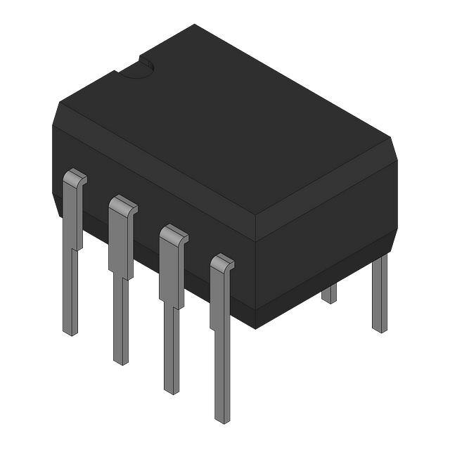
PART NUMBER HA7-5135-5 TEMP. RANGE (oC) 0 to 75 PACKAGE 8 Ld CERDIP PKG. NO. F8.3A
Pinout
HA-5135 (CERDIP) TOP VIEW
BAL -IN +IN V-
1 2 3 4
8 BAL 1
+
7 V+ 6 OUT 5 BAL 1
NOTE: Both BAL 1 pins are connected together internally.
1
CAUTION: These devices are sensitive to electrostatic discharge; follow proper IC Handling Procedures. 1-888-INTERSIL or 321-724-7143 | Intersil (and design) is a registered trademark of Intersil Americas Inc. Copyright © Intersil Americas Inc. 2004. All Rights Reserved All other trademarks mentioned are the property of their respective owners.
�HA-5135
Absolute Maximum Ratings
Voltage Between V+ and V- Terminals . . . . . . . . . . . . . . . . . . . 40V Differential Input Voltage . . . . . . . . . . . . . . . . . . . . . . . . . . . . . . . 7V Output Short Circuit Duration. . . . . . . . . . . . . . . . . . . . . . . Indefinite
Thermal Information
Thermal Resistance (Typical, Note 2) θJA (oC/W) θJC (oC/W) CERDIP Package. . . . . . . . . . . . . . . . . 115 28 Maximum Junction Temperature (Note 1) . . . . . . . . . . . . . . . . 175oC Maximum Storage Temperature Range . . . . . . . . . -65oC to 150oC Maximum Lead Temperature (Soldering 10s) . . . . . . . . . . . . 300oC
Operating Conditions
Temperature Ranges HA-5135-5 . . . . . . . . . . . . . . . . . . . . . . . . . . . . . . . . 0oC to 75oC
CAUTION: Stresses above those listed in “Absolute Maximum Ratings” may cause permanent damage to the device. This is a stress only rating and operation of the device at these or any other conditions above those indicated in the operational sections of this specification is not implied.
NOTES: 1. Maximum power dissipation, including output load, must be designed to maintain the maximum junction temperature below 175oC. 2. θJA is measured with the component mounted on an evaluation PC board in free air.
Electrical Specifications
PARAMETER INPUT CHARACTERISTICS Offset Voltage
VSUPPLY = ±15V TEMP. (oC) HA-5135-5 MIN TYP MAX UNITS
TEST CONDITIONS
25 Full
±12 20 -
10 50 0.4 ±1 0.02 0.02 30 13.0 10.0 9.0 15 0.4 0.17 0.14
75 130 1.3 ±4 ±6 0.04 4 5.5 0.04 0.6 18.0 13.0 11.0 30 0.8 0.23 0.17
µV µV µV/oC nA nA nA/oC nA nA nA/oC V MΩ µVP-P nV/√Hz nV/√Hz nV/√Hz pAP-P pA/√Hz pA/√Hz pA/√Hz
Average Offset Voltage Drift Bias Current
Full 25 Full
Bias Current Average Drift Offset Current
Full 25 Full
Offset Current Average Drift Common Mode Range Differential Input Resistance Input Noise Voltage (Note 3) Input Noise Voltage Density (Note 3) 0.1Hz to 10Hz f = 10Hz f = 100Hz f = 1000Hz Input Noise Current (Note 3) Input Noise Current Density (Note 3) 0.1Hz to 10Hz f = 10Hz f = 100Hz f = 1000Hz TRANSFER CHARACTERISTICS Large Signal Voltage Gain VOUT = ±10V, RL = 2kΩ
Full Full 25 25 25
25 25
-
25 Full
120 120 106 0.6
140 120 2.5
-
dB dB dB MHz
Common Mode Rejection Ratio Closed Loop Bandwidth OUTPUT CHARACTERISTICS Output Voltage Swing
VCM = ±10V AVCL = +1
Full 25
RL = 600Ω
25 Full
±10 ±10
±12 -
-
V V
2
�HA-5135
Electrical Specifications
PARAMETER Full Power Bandwidth (Note 4) Output Current Output Resistance TRANSIENT RESPONSE (Note 6) Rise Time Slew Rate Settling Time (Note 7) POWER SUPPLY CHARACTERISTICS Supply Current Power Supply Rejection Ratio NOTES: 3. Not tested. 90% of units meet or exceed these specifications. Slew Rate 4. Full power bandwidth guaranteed based on slew rate measurement using: FPBW = ------------------------------ . 2 π V PEAK 5. Output resistance measured under open loop conditions (f = 100Hz). 6. Refer to test circuits section of the data sheet. 7. Settling time is measured to 0.1% of final value for a 10V output step and AV = -1. VS = ±5V to ±20V Full Full 94 1.0 130 1.7 mA dB 25 25 25 0.5 340 0.8 11 ns V/µs µs VSUPPLY = ±15V (Continued) TEMP. (oC) 25 25 25 HA-5135-5 MIN 8 ±15 TYP 10 ±20 45 MAX UNITS kHz mA Ω
TEST CONDITIONS RL = 2k Ω VOUT = 10V Note 5
Test Circuits and Waveforms
IN +
2kΩ
OUT 100pF
FIGURE 1. SLEW RATE AND TRANSIENT RESPONSE TEST CIRCUIT
INPUT
0V
INPUT
0V
OUTPUT
0V
OUTPUT
0V
Vertical Scale: Input = 50mV/Div. Output = 100mV/Div. Horizontal Scale: 1µs/Div. SMALL SIGNAL RESPONSE
Vertical Scale: 5V/Div. Horizontal Scale: 5µs/Div. LARGE SIGNAL RESPONSE
3
�HA-5135 Test Circuits and Waveforms
(Continued)
+15V 2N4416 5kΩ 5kΩ +15V + A.U.T. VIN 2kΩ VOUT 100pF -15V 2kΩ TO OSCILLOSCOPE 2kΩ
NOTES: 8. AV = -1. 9. Feedback and summing resistors should be 0.1% matched. 10. Clipping diodes are optional. HP5082-2810 recommended.
-
FIGURE 2. SETTLING TIME CIRCUIT
Schematic Diagram
BALANCE V+ R9 R5 R10 R11 R12 R8 Q36 C2 Q44 Q55 Q35 Q21 Q19 C3 Q8 Q17 Q22 RP18 Q15 Q13 Q46 R19 R3 Q3 (-) INVERTING INPUT Q1 Q11 Q9 Q10 Q16 Q12 Q6 Q5 Q2 Q4 Q14 R4 (+) NONINVERTING INPUT Q52 Q7 Q26 Q42 Q51 Q49 R20 Q41 R13 Q53 R14 Q25 R2 R17 VC1 Q31 Q45 C4 Q24 Q30 Q34 Q18 Q54 Q40 Q39 Q27 R15 R7 Q56 R6 Q57 Q20 Q37 Q58 Q43 Q38 Q28 Q32 Q47 Q33
R16
OUT
Q50 Q48 Z1
4
�HA-5135 Application Information
Power Supply Decoupling
Although not absolutely necessary, it is recommended that all power supply lines be decoupled with 0.01µF ceramic capacitors to ground. Decoupling capacitors should be located as near to the amplifier terminals as possible.
Saturation Recovery
Input and output saturation recovery time is negligible in most applications. However, care should be exercised to avoid exceeding the absolute maximum ratings of the device.
Considerations For Prototyping:
The following list of recommendations are suggested for prototyping. 1. Resolving low level signals requires minimizing leakage currents caused by external circuitry. Use of quality insulating materials, thorough cleaning of insulating surfaces and implementation of moisture barriers when required is suggested. 2. Error voltages generated by thermocouples formed between dissimilar metals in the presence of temperature gradients should be minimized. Isolation of low level circuity from heat generating components is recommended. 3. Shielded cable input leads, guard rings and shield drivers are recommended for the most critical applications.
Differential Input Voltages
Inputs are shunted with back-to-back diodes for overvoltage protection. In applications where differential input voltages in excess of 1V are applied between the inputs, the use of limiting resistors at the inputs is recommended.
Typical Applications
The excellent input and gain characteristics of HA-5135 are well suited for precision integrator applications. Accurate integration over seven decades of frequency using HA-5135, virtually nullifies the need for more expensive chopper-type amplifiers.
C
Large Capacitive Loads
When driving large capacitive loads (>500pF), a small value resistor (≈50Ω) should be connected in series with the output and inside the feedback loop.
8 1 R 2 7
Offset Voltage Adjustment (See Figure 3)
A 20kΩ balance potentiometer is recommended if offset nulling is required. However, other potentiometer values such as 10kΩ, 50kΩ and 100kΩ may be used. The minimum adjustment range for given values is ±2mV. VOS TC of the amplifier is optimized at minimal VOS. Tested Offset Adjustment is |VOS + 1mV| minimum referred to output.
V+ RP (NOTE) 20kΩ 8 1 7 OPTIONAL CONNECTION 6
+
6
OUT
3 4 RB
5
FIGURE 4. PRECISION INTEGRATOR
Low VOS coupled with high open loop Gain, high CMRR and high PSRR make HA-5135 ideally suited for precision detector applications, such as the zero crossing detector shown in Figure 5.
2
+
3 4
5
FIGURE 3. OFFSET NULLING CONNECTIONS
5
�HA-5135
8 OUTPUT ±13V 200µs/DIV. INPUT 2 RIN 3 INPUT ±5mV 200µs/DIV. 4 RF 5 1 7
+
6
OUT
OPTIONAL FOR OUTPUT SWING LIMITING
FIGURE 5. ZERO CROSSING DETECTOR
HA-5135 + 2kΩ +15V
-
4.5kΩ 2kΩ 500Ω +15V + + HA-5135
-
4.5kΩ
2kΩ
-15V 2kΩ
-
HA-5135 -15V
NOTE: AV = 100
FIGURE 6. PRECISION INSTRUMENTATION AMPLIFIER
Typical Performance Curves
INPUT BIAS CURRENT (nA) 4 80 INPUT OFFSET VOLTAGE (µV) 70 60 50 40 30 20 10 0 -80 -40 0 40 80 TYPICAL |VOS| INPUT OFFSET CURRENT INPUT BIAS CURRENT 3 2 1 0 4 INPUT OFFSET CURRENT (nA) 2 0 -2 -4 160
6 4 2 0 -2 -4 -6
120
BIAS CURRENT (nA)
TEMPERATURE (oC)
-10
-8
-4 -2 -6 0 2 4 6 DIFFERENTIAL INPUT VOLTAGE (V)
8
10
FIGURE 7. INPUT OFFSET VOLTAGE, INPUT BIAS AND OFFSET CURRENT vs TEMPERATURE
FIGURE 8. INPUT BIAS CURRENT vs DIFFERENTIAL INPUT VOLTAGE
6
�HA-5135 Typical Performance Curves
VSUPPLY = ±15V TC = ±1oC, AV = 1000 10 5 0 -5 -10 MEASUREMENT AND ENVIRONMENTAL SYSTEMS ALLOWED 12 HOUR STABILIZATION PERIOD
(Continued)
14 INPUT NOISE VOLTAGE (nV/√Hz) 12 10 8 6 4 NOISE CURRENT 2 0 0.2 0 10 100 1K 10K 100K FREQUENCY (Hz) NOISE VOLTAGE 1.4 INPUT NOISE CURRENT (pA/√Hz) 1.2 1.0 0.8 0.6 0.4
TOTAL DRIFT WITH TIME (µV)
2 4 6 8 10
20 30 TIME (DAYS)
40
FIGURE 9. HA-5135 OFFSET VOLTAGE STABILITY vs TIME
FIGURE 10. INPUT NOISE vs FREQUENCY
160 OPEN LOOP VOLTAGE GAIN (dB) 140
0 80 CLOSED LOOP GAIN (dB) 45 PHASE (DEGREES) 70 60 50 40 30 20 10 0 -10 1 10 100 1K 10K 100K 1M 10M 1 10 100 1K 10K 100K 1M 10M FREQUENCY (Hz) FREQUENCY (Hz)
120 100 80 60 GAIN 40 20 0 -20 PHASE ANGLE
90
135
180
FIGURE 11. OPEN LOOP FREQUENCY RESPONSE
FIGURE 12. CLOSED LOOP FREQUENCY RESPONSE
35 OUTPUT VOLTAGE SWING (VP-P) VSUPPLY = ±20V 30 VSUPPLY = ±15V 25 20 15 10 VSUPPLY = ±5V 5 RL = 2kΩ 60 PHASE MARGIN (DEGREES) UNITY GAIN BANDWIDTH (MHz) 50 PHASE MARGIN 40 30 20 BANDWIDTH 10 0 10 2.4 2.35 100 1000 10,000 LOAD CAPACITANCE (pF) 2.5 2.6
VSUPPLY = ±10V
100
1K
10K FREQUENCY (Hz)
100K
1M
FIGURE 13. SMALL SIGNAL BANDWIDTH AND PHASE MARGIN vs LOAD CAPACITANCE
FIGURE 14. OUTPUT VOLTAGE SWING vs FREQUENCY
7
�HA-5135 Typical Performance Curves
30 OUTPUT VOLTAGE SWING (VP-P) 25 20 VSUPPLY = ±10V 15 10 5 0 1 10 100 1K 10K LOAD RESISTANCE (Ω) NORMALIZED AC PARAMETERS REFERRED TO VALUE AT ±15V VSUPPLY = ±15V
(Continued)
1.1 BANDWIDTH
1.0
0.9 SLEW RATE 0.8
VSUPPLY = ±5V
0.7
0.6 0 2 4 6 8 10 12 14 16 18 20 SUPPLY VOLTAGE (±V)
FIGURE 15. MAXIMUM OUTPUT VOLTAGE SWING vs LOAD RESISTANCE
FIGURE 16. NORMALIZED AC PARAMETERS vs SUPPLY VOLTAGE
140 120 100 CMRR (dB) 80 60 40 20 0 1 10 100 1K 10K 100K FREQUENCY (Hz) PSRR (dB)
140 120 100 80 60 40 20 0 1 10 100 1K 10K 100K FREQUENCY (Hz)
FIGURE 17. CMRR vs FREQUENCY
FIGURE 18. PSRR vs FREQUENCY
10
±1.4 TO 10mV ±1.2 SUPPLY CURRENT (mA) TO 1mV ±1.0 VS = ±20V ±0.8 ±0.6 ±0.4 ±0.2 0 -80 VS = ±15V VS = ±10V VS = ±5V
OUTPUT VOLTAGE STEP - VOLTS FROM 0 VOLTS
5
0
-5 TO 10mV -10 0 2 4 6
TO 1mV
8
10
12
14
16
-40
0
40
80
120
160
SETTLING TIME (µs)
TEMPERATURE (oC)
FIGURE 19. SETTLING TIME FOR VARIOUS OUTPUT STEP VOLTAGES
FIGURE 20. POWER SUPPLY CURRENT vs TEMPERATURE
8
�HA-5135 Die Characteristics
DIE DIMENSIONS: 72 mils x 103 mils x 19 mils (1840µm x 2620µm x 483µm) METALLIZATION: Type: Al, 1% Cu Thickness: 16kÅ ±2kÅ SUBSTRATE POTENTIAL (POWERED UP): VPASSIVATION: Type: Nitride (Si3N4) over Silox (SiO2, 5% Phos.) Silox Thickness: 12kÅ ±2kÅ Nitride Thickness: 3.5kÅ ±1.5kÅ TRANSISTOR COUNT: 71 PROCESS: Bipolar Dielectric Isolation
Metallization Mask Layout
HA-5135O
BAL1
V+
OUT
BAL1
BAL2
-IN
+IN
V-
9
�HA-5135 Ceramic Dual-In-Line Frit Seal Packages (CERDIP)
c1 -A-DBASE METAL E b1 M -Bbbb S BASE PLANE SEATING PLANE S1 b2 b ccc M C A-B S AA C A-B S D Q -CA L DS M (b) SECTION A-A (c) LEAD FINISH
F8.3A MIL-STD-1835 GDIP1-T8 (D-4, CONFIGURATION A)
8 LEAD CERAMIC DUAL-IN-LINE FRIT SEAL PACKAGE INCHES SYMBOL A b b1 b2 b3 c MIN 0.014 0.014 0.045 0.023 0.008 0.008 0.220 MAX 0.200 0.026 0.023 0.065 0.045 0.018 0.015 0.405 0.310 MILLIMETERS MIN 0.36 0.36 1.14 0.58 0.20 0.20 5.59 MAX 5.08 0.66 0.58 1.65 1.14 0.46 0.38 10.29 7.87 NOTES 2 3 4 2 3 5 5 6 7 2, 3 8 Rev. 0 4/94
α
eA
c1 D E e eA eA/2 L Q S1
e
DS
eA/2
c
0.100 BSC 0.300 BSC 0.150 BSC 0.125 0.015 0.005 90o 8 0.200 0.060 105o 0.015 0.030 0.010 0.0015
2.54 BSC 7.62 BSC 3.81 BSC 3.18 0.38 0.13 90o 8 5.08 1.52 105o 0.38 0.76 0.25 0.038
aaa M C A - B S D S
NOTES: 1. Index area: A notch or a pin one identification mark shall be located adjacent to pin one and shall be located within the shaded area shown. The manufacturer’s identification shall not be used as a pin one identification mark. 2. The maximum limits of lead dimensions b and c or M shall be measured at the centroid of the finished lead surfaces, when solder dip or tin plate lead finish is applied. 3. Dimensions b1 and c1 apply to lead base metal only. Dimension M applies to lead plating and finish thickness. 4. Corner leads (1, N, N/2, and N/2+1) may be configured with a partial lead paddle. For this configuration dimension b3 replaces dimension b2. 5. This dimension allows for off-center lid, meniscus, and glass overrun. 6. Dimension Q shall be measured from the seating plane to the base plane. 7. Measure dimension S1 at all four corners. 8. N is the maximum number of terminal positions. 9. Dimensioning and tolerancing per ANSI Y14.5M - 1982. 10. Controlling dimension: INCH
α
aaa bbb ccc M N
All Intersil U.S. products are manufactured, assembled and tested utilizing ISO9000 quality systems. Intersil Corporation’s quality certifications can be viewed at www.intersil.com/design/quality
Intersil products are sold by description only. Intersil Corporation reserves the right to make changes in circuit design, software and/or specifications at any time without notice. Accordingly, the reader is cautioned to verify that data sheets are current before placing orders. Information furnished by Intersil is believed to be accurate and reliable. However, no responsibility is assumed by Intersil or its subsidiaries for its use; nor for any infringements of patents or other rights of third parties which may result from its use. No license is granted by implication or otherwise under any patent or patent rights of Intersil or its subsidiaries.
For information regarding Intersil Corporation and its products, see www.intersil.com 10
�
很抱歉,暂时无法提供与“HA7-5135-5”相匹配的价格&库存,您可以联系我们找货
免费人工找货