IXTT40N50L2
IXTQ40N50L2
IXTH40N50L2
LinearL2TM
Power MOSFET
w/Extended FBSOA
VDSS
ID25
= 500V
= 40A
170m
RDS(on)
N-Channel Enhancement Mode
Avalanche rated
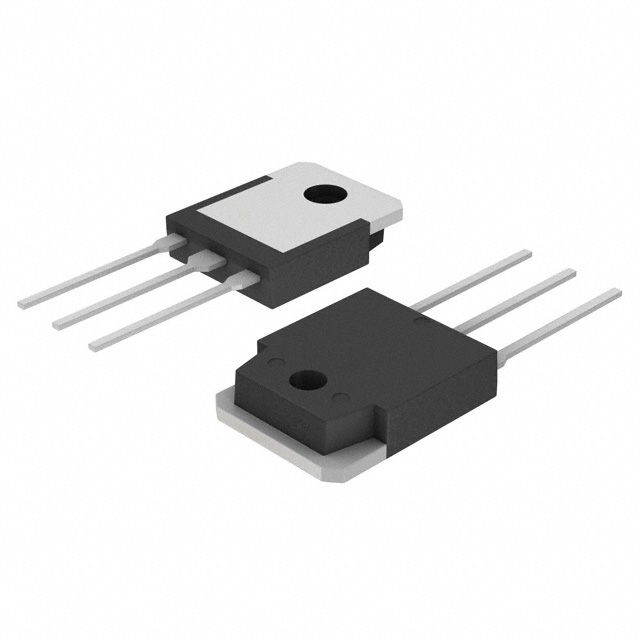
TO-268 (IXTT)
G
S
D (Tab)
TO-3P (IXTQ)
Symbol
Test Conditions
Maximum Ratings
VDSS
TJ = 25C to 150C
500
V
VDGR
TJ = 25C to 150C, RGS = 1M
500
V
VGSS
Continuous
20
V
VGSM
Transient
30
V
ID25
TC = 25C
40
A
IDM
TC = 25C, Pulse Width Limited by TJM
80
A
IA
TC = 25C
40
A
EAS
TC = 25C
2
J
PD
TC = 25C
540
W
-55 to +150
C
TJM
+150
C
Tstg
-55 to +150
C
300
260
°C
°C
1.13/10
Nm/lb.in
4.0
5.5
6.0
g
g
g
TJ
TL
TSOLD
Maximum Lead Temperature for Soldering
1.6 mm (0.062in.) from Case for 10s
Md
Mounting Torque (TO-247&TO-3P)
Weight
TO-268
TO-3P
TO-247
G
D
G
VGS = 0V, ID = 1mA
500
VGS(th)
VDS = VGS, ID = 250A
2.5
IGSS
VGS = 20V, VDS = 0V
IDSS
VDS = VDSS, VGS = 0V
TJ = 125C
RDS(on)
VGS = 10V, ID = 0.5 • ID25, Note 1
© 2017 IXYS CORPORATION, All rights reserved
V
4.5
V
100
nA
S
D (Tab)
D
= Drain
Tab = Drain
Features
BVDSS
D
G = Gate
S = Source
Characteristic Values
Min.
Typ.
Max.
D (Tab)
TO-247 (IXTH)
Symbol
Test Conditions
(TJ = 25C, Unless Otherwise Specified)
S
Designed for Linear Operation
International Standard Packages
Avalanche Rated
Molding Epoxies Meet UL 94 V-0
Flammability Classification
Guaranteed FBSOA at 75C
Applications
50
A
300
A
170 m
Solid State Circuit Breakers
Soft Start Controls
Linear Amplifiers
Programmable Loads
Current Regulators
DS100100B(6/17)
�IXTT40N50L2
Symbol
Test Conditions
(TJ = 25C, Unless Otherwise Specified)
gfs
Characteristic Values
Min.
Typ.
Max.
VDS = 10V, ID = 0.5 • ID25, Note 1
11
VGS = 0V, VDS = 25V, f = 1MHz
Crss
td(on)
tr
td(off)
tf
Resistive Switching Times
VGS = 10V, VDS = 0.5 • VDSS, ID = 0.5 • ID25
RG = 2 (External)
Qg(on)
Qgs
15
VGS = 10V, VDS = 0.5 • VDSS, ID = 0.5 • ID25
Qgd
S
nF
655
pF
155
pF
50
ns
133
ns
127
ns
44
ns
320
nC
64
nC
198
nC
0.23 C/W
RthJC
RthCS
19
10.4
Ciss
Coss
IXTQ40N50L2
IXTH40N50L2
(TO-247&TO-3P)
C/W
0.25
Safe Operating Area Specification
Symbol
Test Conditions
Min.
SOA
VDS = 400V, ID = 0.8A, TC = 75°C, tp = 3s
320
Typ.
Max.
W
Source-Drain Diode
Symbol
Test Conditions
(TJ = 25C, Unless Otherwise Specified)
IS
VGS = 0V
ISM
Characteristic Values
Min.
Typ.
Max.
40
A
Repetitive, Pulse Width Limited by TJM
160
A
VSD
IF = IS, VGS = 0V, Note 1
1.5
V
trr
IF = IS, -di/dt = 100A/μs, VR = 100V
500
ns
Note 1: Pulse test, t 300s, duty cycle, d 2%.
IXYS reserves the right to change limits, test conditions, and dimensions.
IXYS MOSFETs and IGBTs are covered
4,835,592
by one or more of the following U.S. patents: 4,860,072
4,881,106
4,931,844
5,017,508
5,034,796
5,049,961
5,063,307
5,187,117
5,237,481
5,381,025
5,486,715
6,162,665
6,259,123 B1
6,306,728 B1
6,404,065 B1
6,534,343
6,583,505
6,683,344
6,727,585
7,005,734 B2
6,710,405 B2 6,759,692
7,063,975 B2
6,710,463
6,771,478 B2 7,071,537
7,157,338B2
�IXTT40N50L2
o
o
Fig. 1. Output Characteristics @ TJ = 25 C
Fig. 2. Extended Output Characteristics @ TJ = 25 C
40
100
VGS = 20V
VGS = 20V
12V
10V
35
12V
9V
80
25
I D - Amperes
30
I D - Amperes
IXTQ40N50L2
IXTH40N50L2
8V
20
15
10V
60
9V
40
7V
8V
10
20
7V
6V
5
5V
0
0
1
2
3
4
5
6
6V
5V
0
7
8
0
5
10
15
VDS - Volts
25
30
Fig. 4. RDS(on) Normalized to ID = 20A Value vs.
Junction Temperature
o
Fig. 3. Output Characteristics @ TJ = 125 C
40
2.8
VGS = 20V
12V
10V
9V
30
VGS = 10V
2.4
RDS(on) - Normalized
35
I D - Amperes
20
VDS - Volts
8V
25
20
7V
15
I D = 40A
2.0
I D = 20A
1.6
1.2
10
6V
0.8
5
5V
0
0
2
4
6
8
10
12
0.4
14
-50
16
-25
0
25
50
75
100
125
150
125
150
TJ - Degrees Centigrade
VDS - Volts
Fig. 5. RDS(on) Normalized to ID = 20A Value vs.
Drain Current
Fig. 6. Maximum Drain Current vs.
Case Temperature
45
o
VGS = 10V
2.8
TJ = 125 C
40
30
I D - Amperes
RDS(on) - Normalized
35
2.4
2.0
o
TJ = 25 C
1.6
25
20
15
10
1.2
5
0.8
0
0
10
20
30
40
50
I D - Amperes
© 2017 IXYS CORPORATION, All rights reserved
60
70
80
90
-50
-25
0
25
50
75
TC - Degrees Centigrade
100
�IXTT40N50L2
IXTQ40N50L2
IXTH40N50L2
Fig. 8. Transconductance
Fig. 7. Input Admittance
36
70
o
TJ = - 40 C
60
30
o
25 C
50
40
24
g f s - Siemens
I D - Amperes
o
TJ = 125 C
o
25 C
o
- 40 C
30
o
125 C
18
12
20
6
10
0
0
3
4
5
6
7
8
9
0
10
10
20
30
VGS - Volts
50
60
70
Fig. 10. Gate Charge
Fig. 9. Forward Voltage Drop of Intrinsic Diode
16
120
VDS = 250V
14
I D = 20A
100
I G = 10mA
12
V GS - Volts
80
I S - Amperes
40
I D - Amperes
60
40
10
8
6
o
TJ = 125 C
4
o
TJ = 25 C
20
2
0
0
0.4
0.5
0.6
0.7
0.8
0.9
1.0
1.1
0
50
100
VSD - Volts
150
200
250
300
350
400
450
QG - NanoCoulombs
Fig. 12. Maximum Transient Thermal Impedance
Fig. 11. Capacitance
1
100,000
Capacitance - PicoFarads
f = 1 MHz
Z (th)JC - K / W
10,000
Ciss
Coss
0.1
0.01
1,000
Crss
100
0
5
10
15
20
25
30
35
40
VDS - Volts
IXYS reserves the right to change limits, test conditions, and dimensions.
0.001
0.00001
0.0001
0.001
0.01
0.1
Pulse Width - Seconds
1
10
�IXTT40N50L2
Fig. 14. Forward-Bias Safe Operating Area
Fig. 13. Forward-Bias Safe Operating Area
o
o
@ TC = 25 C
100
IXTQ40N50L2
IXTH40N50L2
@ TC = 75 C
100
RDS(on) Limit
RDS(on) Limit
25μs
25μs
100μs
100μs
10
10
I D - Amperes
I D - Amperes
1ms
10ms
100ms
1
1ms
10ms
1
DC
DC
TJ = 150oC
100ms
TJ = 150oC
o
TC = 75oC
Single Pulse
TC = 25 C
Single Pulse
0.1
0.1
10
100
1000
10
TO-3P Outline
TO-268 Outline
100
1000
VDS - Volts
VDS - Volts
TO-247 Outline
A
A2
E
0P
0P1
E1
D
A
A2
A2
Q
S
+
+
D1
D
2
L1
D2
0P1
1
3
S
+
D1
D
4
1
+
R
+
A
0P O
+ 0K M D B M
B
E
2
3
4
ixys option
L1
C
A1
E1
L
A1
Terminals: 1 - Gate
3 - Source
2,4 - Drain
b
b2
c
b4
e
PINS: 1 - Gate
2, 4 - Drain
3 - Source
© 2017 IXYS CORPORATION, All rights reserved
c
b
b2
b4
e
+ J M C AM
O
PINS: 1 - Gate
2, 4 - Drain
3 - Source
IXYS REF: T_40N50L2(8R)6-16-17-B
�Disclaimer Notice - Information furnished is believed to be accurate and reliable. However, users should independently
evaluate the suitability of and test each product selected for their own applications. Littelfuse products are not designed for,
and may not be used in, all applications. Read complete Disclaimer Notice at www.littelfuse.com/disclaimer-electronics.
�


 工商网监
湘ICP备2023018690号
工商网监
湘ICP备2023018690号
