JIANGSU CHANGJIANG ELECTRONICS TECHNOLOGY CO., LTD
1A LOW DROPOUT LINEAR REGULATOR
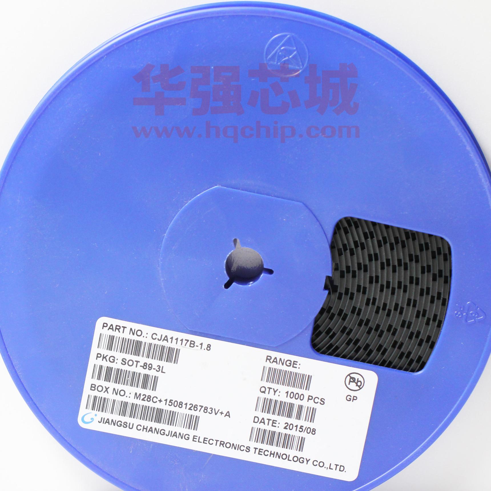
CJA1117B-XXX
SOT-89-3L
FEATURES
Low Dropout Voltage: 1.15V at 1A Output Current
Trimmed Current Limit
1. ADJ/GND
On-Chip Thermal Shutdown
2. OUTPUT
Three-Terminal Adjustable or Fixed 1.8V, 2.5V, 3.3V, 5V
3.IN
Operation Junction Temperature: -25 ℃ to 125℃
GENERAL DESCRIPTION
The CJA1117B-XXX is a series of low dropout three-terminal regulators with a dropout of 1.15V at
1A output current.
The CJA1117B-XXX series provides current limiting and thermal shutdown. Its circuit includes a
trimmed bandage. reference to assure output voltage accuracy to be within 1.5%. Current limit is
trimmed to ensure specified. output current and controlled short-circuit current. On-chip thermal
shutdown provides protection against any combination of overload and ambient temperature that would
create excessive junction temperature.
The CJA1117B-XXX has an adjustable version, that can provide the output voltage from 1.25V to 5V with
only 2 external resistors.
APPLICATIONS
PC Motherboard
LCD Monitor
Graphic Card
DVD-Video Player
NIC/Switch
Telecom Modem
ADSL Modem
Printer and other peripheral Equipment
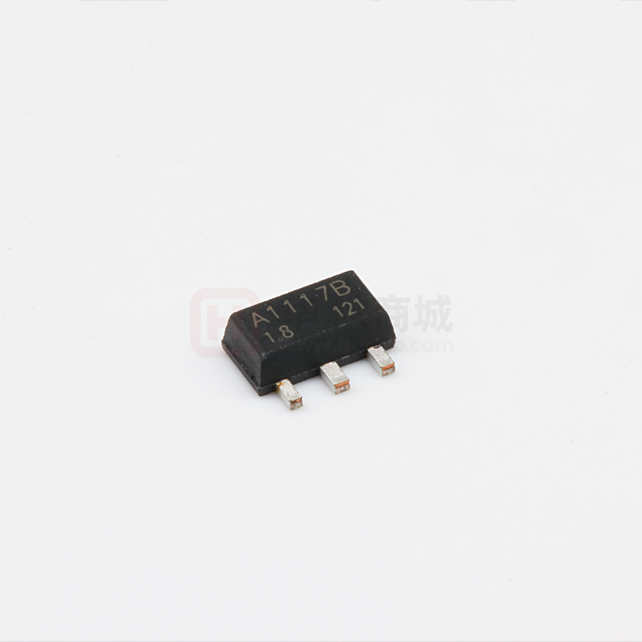
Marking:
A1117B
��� 121
www.cj-elec.com
1
E,Mar,2016
�ORDERING INFORMATION
Package
Operating Junction Temperature Range
Part NO.
CJA1117B-ADJ
CJA1117B-1.8
SOT-89-3L
-25 to 125℃
CJA1117B-2.5
CJA1117B-3.3
CJA1117B-5.0
ABOSLUTE MAXIMUM RATINGS (Ta=25℃ unless otherwise noted)
Parameter
Symbol
Value
Unit
Vi
20
V
Input Voltage
Tj
150
℃
Tstg
RθJA
-55~+150
250
℃
℃/W
TL
260
℃
VESD
400
V
Maximum Junction Temperature
Storage Temperature
Thermal Resistance from Junction to Ambient
Lead Temperature (Soldering, 10sec.)
ESD Voltage (Machine Model)
Note: Stresses greater than those listed under ”Absolute Maximum Ratings” may cause permanent
damage to the device. These are stress ratings only, and functional of the device at these or any other
conditions beyond those indicated under “Recommended Operating Conditions” is not implied. Exposure
to “Absolute Maximum Ratings” for extended periods may affect device reliability.
RECOMMENDED OPERATING CONDITIONS
Parameter
Symbol
Value
Unit
Input Voltage
Vi
15
V
Operating Junction Temperature
Tj
-25~+125
www.cj-elec.com
2
℃
E,Mar,2016
�ELECTRICAL CHARACTERISTICS (VIN≤10V, TJ=25℃ unless otherwise specified. )
Parameter
Reference Voltage
Symbol
VIROC
Part NO.
CJA1117B-2.5
VO
CJA1117B-3.3
CJA1117B-5.0
Line Regulation
LNR
conditions
Min
Typ
Max
IOUT=10mA, VIN -VOUT =3.23
1.231
1.250
1.269
10mA≤IOUT≤1A, 2.75V≤VIN -VOUT ≤13.25V
1.225
1.250
1.275
CJA1117B-ADJ
CJA1117B-1.8
Output Voltage
Test
IOUT=10mA, VIN=3.8V
1.773
1.8
1.827
10mA≤IOUT≤1A, 3.3V≤VIN ≤12V
1.764
1.8
1.836
IOUT=10mA, VIN=4.5V
2.463
2.5
2.538
10mA≤IOUT≤1A, 4V≤VIN ≤12V
2.450
2.5
2.550
IOUT=10mA, VIN=5.3V
3.251
3.3
3.350
10mA≤IOUT≤1A, 4.8V≤VIN ≤12V
3.234
3.3
3.366
IOUT=10mA, VIN=7.0V
4.925
5.0
5.075
4.9
5.0
5.1
0.035
0.2
10mA≤IOUT≤1A, 6.5V≤VIN ≤12V
CJA1117B-ADJ
IOUT=10mA, 1.5V≤VIN -VOUT ≤12V
CJA1117B-1.8
IOUT=10mA, 1.5V≤VIN -VOUT ≤10.2V
1
7
CJA1117B-2.5
IOUT=10mA, 1.5V≤VIN -VOUT ≤9.5V
1
7
CJA1117B-3.3
IOUT=10mA, 1.5V≤VIN -VOUT ≤8.7V
1
7
CJA1117B-5.0
IOUT=10mA, 1.5V≤VIN -VOUT ≤7V
1
10
0.2
0.4
CJA1117B-ADJ
LDR
CJA1117B-2.5
VIN-VOUT=1.5V, 10mA≤IOUT ≤1A
10
CJA1117B-3.3
13.2
CJA1117B-5.0
20
Dropout Voltage
VD
ΔVREF=1%, IOUT=1.0A
Current Limit
Ilimit
VIN-VOUT=2V
1.3
1
Adjust Pin Current
Minimum
Load Current
Quiescent Current
Ripple Rejection
IL
1.5V≤VIN -VOUT ≤12V (ADJ only)
Iq
VIN= VOUT+1.25V(ADJ except)
RR
f=120Hz,COUT=22μFTantalum,
VIN-VOUT=3V, IOUT=1A
Temperature Stability
Long-Term Stability
TA=125℃, 1000hrs
RMS Output
TA=25℃, 10Hz≤f ≤10kHz
Noise
(% of VOUT)
V
V
V
V
V
%
mV
%
7.2
CJA1117B-1.8
Load Regulation
Unit
Thermal
Shutdown Hysteresis
60
mV
V
A
60
120
μA
1.7
5
μA
5
10
mA
75
dB
0.5
%
0.3
%
0.003
%
25
℃
* With package soldering to copper area over backside ground plane or internal power plane RθJA can vary from 46 ℃/W to
>90℃/W depending on mounting technique and the size of the copper area
www.cj-elec.com
3
E,Mar,2016
�FUNCTIONAL BLOCK DIAGRAM
TYPICAL APPLICATION CIRCUIT
www.cj-elec.com
4
E,Mar,2016
�SOT-89-3L Package Outline Dimensions
Dimensions In Millimeters
Max
Min
1.400
1.600
0.320
0.520
0.400
0.580
0.350
0.440
4.400
4.600
1.550 REF.
2.300
2.600
3.940
4.250
1.500 TYP.
3.000 TYP.
0.900
1.200
Symbol
A
b
b1
c
D
D1
E
E1
e
e1
L
Dimensions In Inches
Min
Max
0.055
0.063
0.013
0.020
0.016
0.023
0.014
0.017
0.173
0.181
0.061 REF.
0.091
0.102
0.155
0.167
0.060 TYP.
0.118 TYP.
0.035
0.047
SOT-89-3L Suggested Pad Layout
www.cj-elec.com
5
E,Mar,2016
�SOT-89-3L Tape and Reel
www.cj-elec.com
6
E,Mar,2016
�
很抱歉,暂时无法提供与“CJA1117-1.8”相匹配的价格&库存,您可以联系我们找货
免费人工找货- 国内价格
- 1+0.60442
- 100+0.56413
- 300+0.52383
- 500+0.48354
- 2000+0.46339
- 5000+0.45130


 工商网监
湘ICP备2023018690号
工商网监
湘ICP备2023018690号
